Electron-Beam Surface Treatment of Metals and Alloys: Techniques and Trends


Abstract
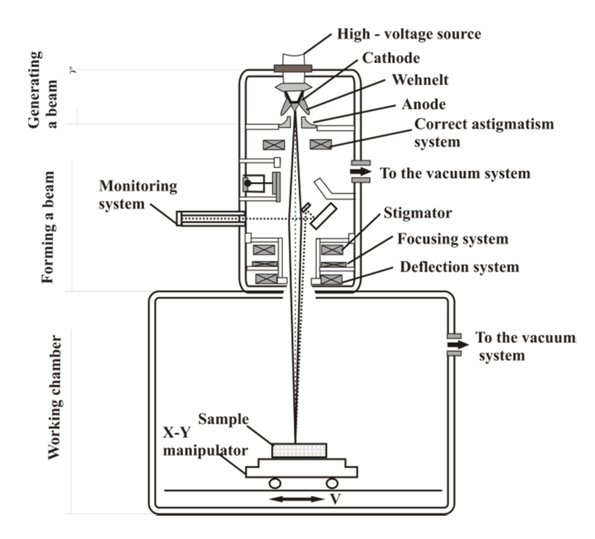
:1. Introduction
- Significantly low cost in comparison with traditional technologies;
- Significantly shorter process time in comparison with traditional technologies;
- Uniform distribution of the energy of the electron beam;
- The technological conditions defined by the technological parameters are highly reproducible.
- Electron-beam surface hardening;
- Combined methods for a surface hardening;
- Electron-beam alloying;
- Electron-beam evaporation and deposition.
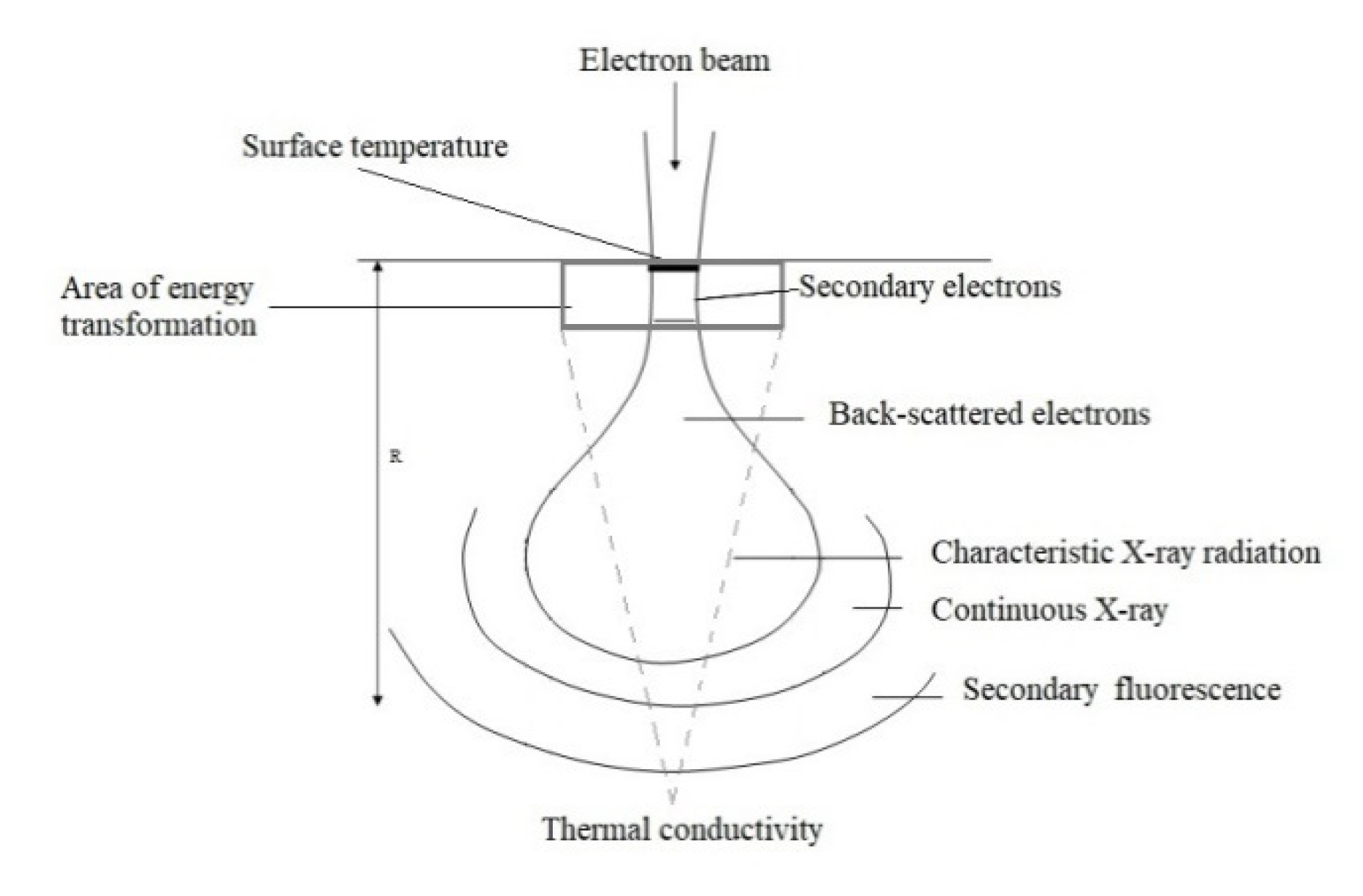
2. Electron-Beam Surface Treatment: Heat Processes
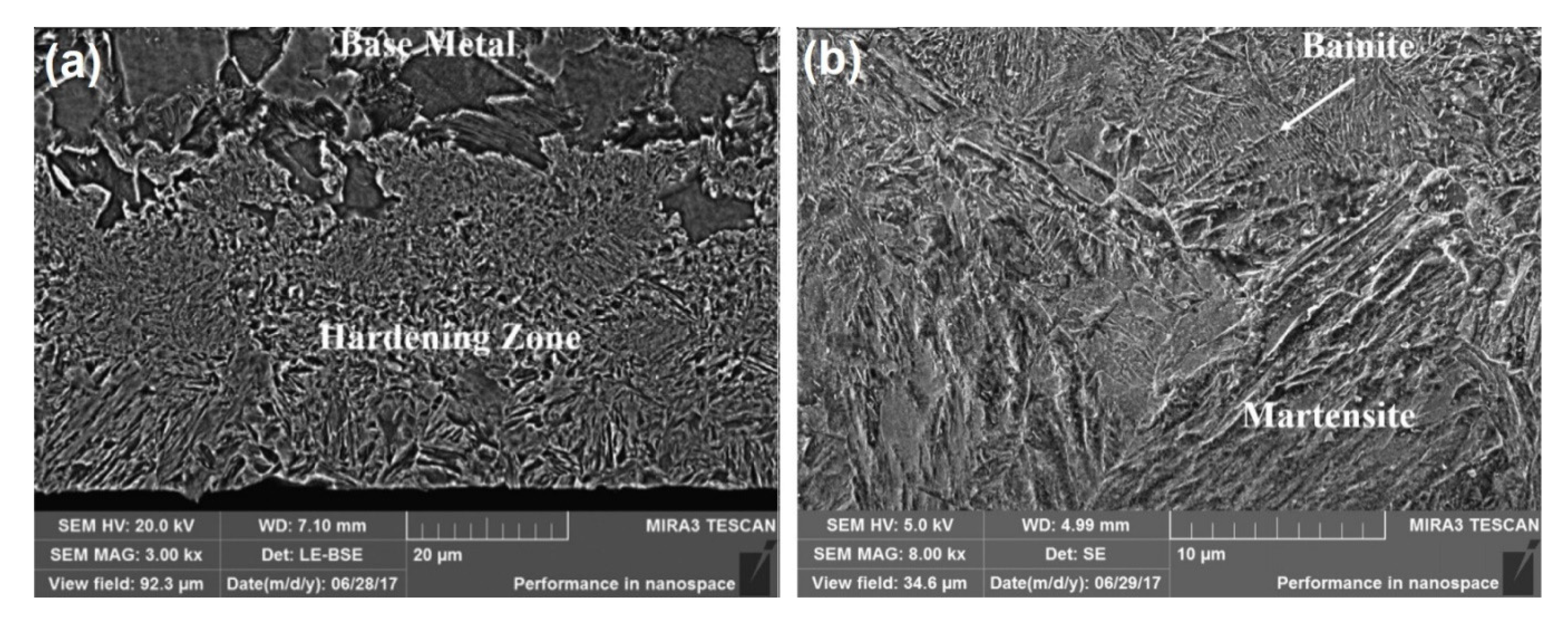
3. Electron-Beam Surface Hardening
4. Combined Methods for a Surface Hardening
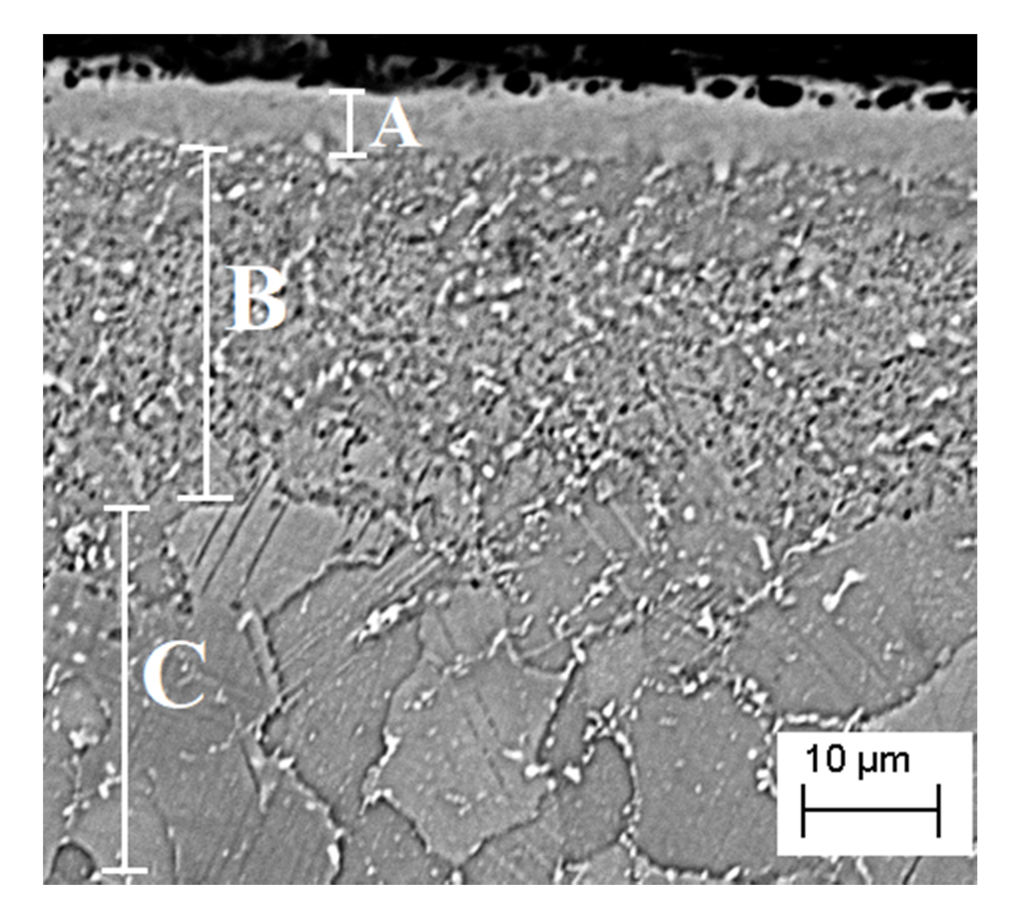
5. Electron-Beam Alloying
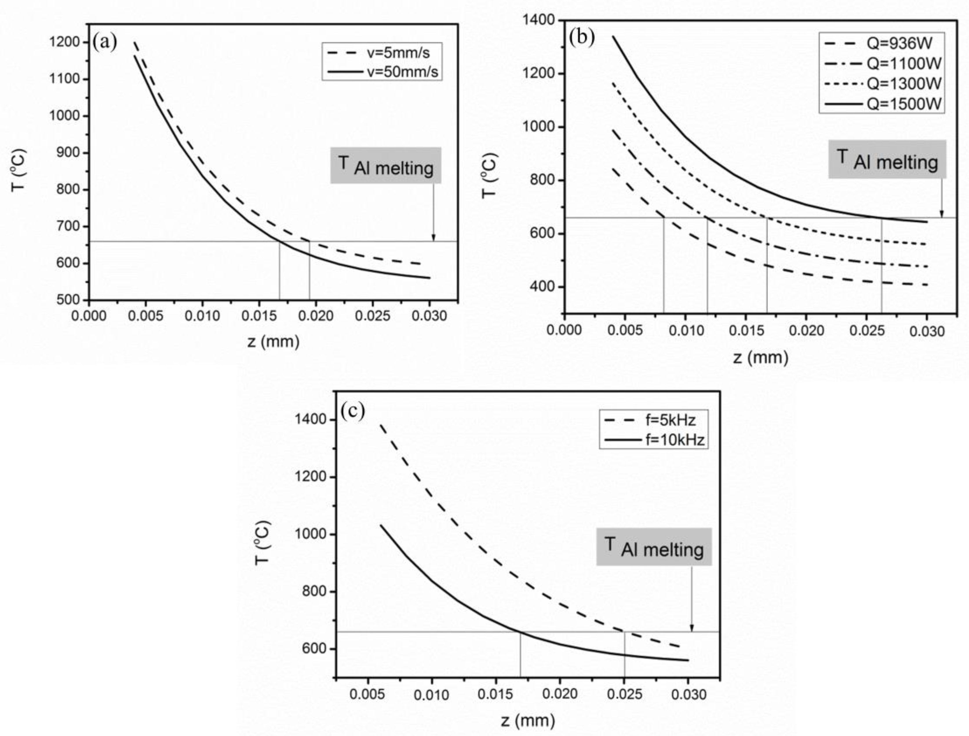
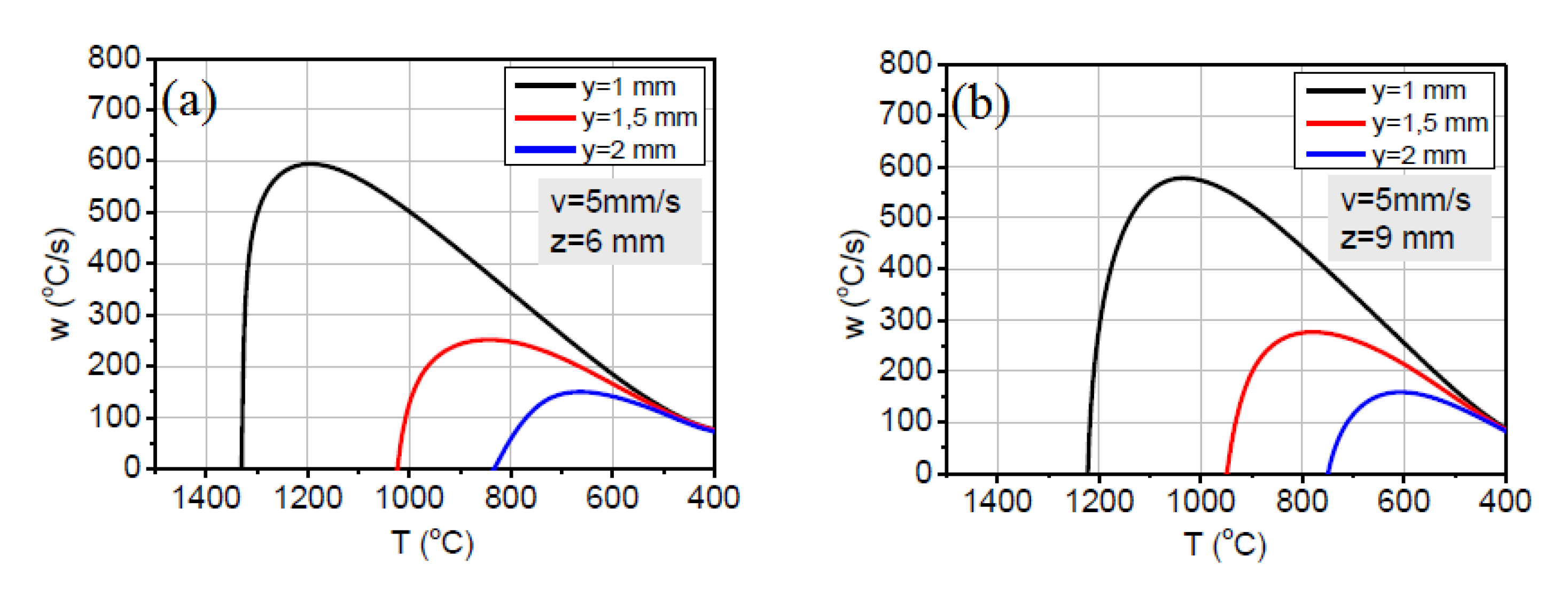
5.1. Electron-Beam Surface Alloying of Aluminum and Its Alloys
5.2. Electron-Beam Surface Alloying of Titanium and Its Alloys
5.3. Electron-Beam Surface Alloying of Other Materials
6. Summary
Author Contributions
Funding
Conflicts of Interest
References
- Yusuf, S.; Cutler, S.; Gao, N. Review: The Impact of Metal Additive Manufacturing on the Aerospace Industry. Metals 2019, 9, 1286. [Google Scholar] [CrossRef] [Green Version]
- Portoles, L.; Jorda, O.; Jorda, L.; Uriondo, A.; Esperson-Miguez, M.; Perinpanayagam, S. A qualification procedure to manufacture and repair aerospace parts with electron beam melting. J. Manuf. Syst. 2016, 41, 65–75. [Google Scholar] [CrossRef]
- Juechter, V.; Franke, M.; Merenda, T.; Stich, A.; Korner, C.; Singer, R. Additive manufacturing of Ti-45Al-4Nb-C by selective electron beam melting for automotive applications. Addit. Manuf. 2018, 22, 118–126. [Google Scholar] [CrossRef]
- Murr, L.; Gaytan, S.; Ceytan, A.; Martinez, E.; Martinez, J.; Hernandez, D.; Machado, B.; Ramirez, D.; Medina, F.; Collins, S.; et al. Characterization of titanium aluminide alloy components fabricated by additive manufacturing using electron beam melting. Acta Mater. 2010, 58, 1887–1894. [Google Scholar] [CrossRef]
- Weglowski, M. Electron beam rapid prototyping using wires and modification of the surface. In Manufacturing Techniques for Materials: Engineering and Engineered, 1st ed.; Srivatsan, T., Sudarshan, T., Manigandan, K., Eds.; Taylor and Francis Group: Boca Raton, FL, USA, 2018; pp. 133–160. [Google Scholar]
- Weglowski, M.; Blacha, S.; Philips, A. Electron beam welding-Techniques and trends-Review. Vacuum 2016, 130, 72–92. [Google Scholar] [CrossRef]
- Abroyan, I.; Andronov, A.; Titov, A. Physical Fundamentals of Electron and Ion Technology; Vysshaya Shkola: Moscow, Russia, 1984. (In Russian) [Google Scholar]
- Schultz, H. Electron Beam Welding; Abington Publishing: Cambridge, UK, 1993. [Google Scholar]
- Petrov, P.; Tongov, M. Numerical modelling of heat source during electron beam welding. Vacuum 2020, 171, 108991. [Google Scholar] [CrossRef]
- Kaisheva, D.; Angelov, V.; Petrov, P. Simulation of heat transfer at welding with oscillating electron beam. Can. J. Phys. 2019, 97, 1140–1146. [Google Scholar] [CrossRef]
- Bishop, C. Electron Beam (E-beam) Evaporation, In Vacuum Deposition onto Webs, Films and Foils; William Andrew: Norwich, NY, USA, 2011; pp. 261–272. [Google Scholar]
- Zou, J.; Qin, Y.; Dong, C.; Wang, X.; Wu, A.; Hao, S. Numerical simulation of the thermal-mechanical process of high current pulsed electron beam treatment. J. Vac. Sci. Technol. A 2004, 22, 545–552. [Google Scholar] [CrossRef]
- Proskurovsky, D.; Rotshtein, V.; Ozur, G.; Markov, A.; Nazarov, D.S. Pulsed electron-beam technology for surface modification of metallic materials. J. Vac. Sci. Technol. A 1998, 16, 2480–2488. [Google Scholar] [CrossRef]
- Panin, A.; Kazachenok, M.; Perevalova, O.; Martynov, S.; Panina, A.; Sklyarova, E. Continuous Electron Beam Post-Treatment of EBF3-Fabricated Ti–6Al–4V Parts. Metals 2019, 9, 699. [Google Scholar] [CrossRef] [Green Version]
- Bocharov, A.; Murygin, A.; Laptenok, V. Calculating the geometric parameters of the distribution of electron beam energy density on its section in EBW. IOP Conf. Ser. Mater. Sci. Eng. 2018, 450, 032010. [Google Scholar] [CrossRef]
- Bohm, S. The Electron Beam as a Tool for Joining Technology; DVS Media GmbH: Düsseldorf, Germany, 2014; pp. 1–100. [Google Scholar]
- Klimpel, A. Welding Handbook; Silesian University of Technology: Gliwice, Poland, 2013; Volume 1, pp. 601–654. [Google Scholar]
- Angelov, V.; Ormanova, M.; Kaisheva, D.; Lazarova, R.; Dimitrova, R.; Petrov, P. Selective electron beam surface alloying of aluminum with TiCN nanoparticles. Nucl. Instrum. Methods Phys. Res. B 2019, 440, 88–94. [Google Scholar] [CrossRef]
- Valkov, S.; Ormanova, M.; Petrov, P. Surface manufacturing of materials by high energy fluxes. In Advanced Surface Engineering Research; Chowdhury, M.A., Ed.; IntechOpen: London, UK, 2018; pp. 69–87. [Google Scholar]
- Schiller, S.; Heisig, U.; Panzer, S. Electron Beam Technology; Willey: Hoboken, NJ, USA, 1982; p. 508. [Google Scholar]
- Farrahi, G.; Sistaninia, M. Thermal analysis of laser hardening for different moving patterns. IJE Trans. A Basics 2009, 22, 169–180. [Google Scholar]
- Ormanova, M.; Angelov, V.; Petrov, P. Investigation of thermal processes at electron-beam surface modification by means of scanning electron beam. J. Phys. Conf. Ser. 2016, 700, 012033. [Google Scholar] [CrossRef] [Green Version]
- Beck, J.; Cole, K.; Haji-Sheikh, A.; Litkouhi, B. Heat Conduction Using Greens Functions, 2nd ed.; Taylor & Francis: Oxfordshire, UK, 2011. [Google Scholar]
- Kaisheva, D. A Study of the Physical Processes at Welding of Materials by High Energy Fluxes. Ph.D. Thesis, Institute of Electronics, Bulgarian Academy of Sciences, Sofia, Bulgaria, 2020. [Google Scholar]
- Zenker, R. Modern thermal electron beam processes—Research results and industrial application. La Metall. Ital. 2009, 101, 1–8. [Google Scholar]
- Dossett, J.; Totten, G. ASM Handbook. In Steel Heat Treating Fundamentals and Processes; ASM International: New York, NY, USA, 2013; Volume 4A. [Google Scholar]
- Wei, D.; Wang, X.; Wang, R.; Cui, H. Surface modification of 5CrMnMo steel with continuous scanning electron beam process. Vacuum 2018, 149, 118–123. [Google Scholar] [CrossRef]
- Fu, Y.; Hu, J.; Shen, X.; Wang, Y.; Zhao, W. Surface hardening of 30CrMnSiA steel using continuous electron beam. Nucl. Instrum. Methods Phys. Res. B 2017, 410, 207–214. [Google Scholar] [CrossRef]
- Petrov, P. Optimization of carbon steel electron-beam hardening. J. Phys. Conf. Ser. 2010, 223, 012029. [Google Scholar] [CrossRef]
- Petrov, P.; Dimitrov, D.; Aprakova, M.; Valkanov, S. Surface Hardening of Alloy Steels Using a High Intensity Electron Beam. Mater. Manuf. Process. 1998, 13, 555–564. [Google Scholar] [CrossRef]
- Zenker, R.; Buchwalder, A. Elektronenstrahl Randschichtbehandlung: Innovative Technologien für höchste industrielle Ansprüche; Pro-beam AG & Co. KGaA: Gilching, Germany, 2010; pp. 1–89. [Google Scholar]
- Song, R.; Zhang, K.; Chen, G. Electron beam surface treatment. Part I: Surface hardening of AISI D3 tool steel. Vacuum 2003, 69, 513–516. [Google Scholar] [CrossRef] [Green Version]
- Gao, Y. Surface modification of TA2 pure titanium by low energy high current pulsed electron beam treatments. Appl. Surf. Sci. 2011, 257, 7455–7460. [Google Scholar] [CrossRef]
- Gao, Y. Influence of pulsed electron beam treatment on microstructure and properties of TA15 titanium alloy. Appl. Surf. Sci. 2013, 264, 633–635. [Google Scholar] [CrossRef]
- Ramskogler, C.; Warchomicka, F.; Mostofi, S.; Weinberg, A.; Sommitsch, C. Innovative surface modification of Ti6Al4V alloy by electron beam technique for biomedical application. Mater. Sci. Eng. C 2017, 78, 105–113. [Google Scholar] [CrossRef] [PubMed]
- Nikolova, M.; Yankov, E.; Petrov, P.; Valkov, S.; Ormanova, M.; Zaharieva, V.; Tonev, D.; Andreeva, A. Electron beam surface modification of Ti5Al4V alloy for biomedical applications. In Proceedings of the METAL 2017—26th International Conference on Metallurgy and Materials, Brno, Czech Republic, 24–26 May 2017; pp. 1555–1560. [Google Scholar]
- Zagulyaev, D.; Konovalov, S.; Gromov, V.; Glezer, A.; Ivanov, Y.; Sundeev, R. Structure and properties changes of Al-Si alloy treated by pulsed electron beam. Mater. Lett. 2018, 229, 377–380. [Google Scholar] [CrossRef]
- Mohandas, T.; Banerjee, D.; Kutumba Rao, V. Fusion zone microstructure and porosity in electron beam welds of an α+β titanium alloy. Metall. Mater. Trans. A 1990, 30A, 789–798. [Google Scholar]
- Dimitrov, D.; Aprakova, M.; Valkanov, S.; Petrov, P. Electron beam hardening of ion nitrided layers. Vacuum 1998, 49, 239–246. [Google Scholar] [CrossRef]
- Zenker, R. Electron meets nitrogen: Combination of electron beam hardening and nitriding. Int. Heat Treat. Surf. Eng. 2009, 3, 141–146. [Google Scholar] [CrossRef]
- Ormanova, M.; Petrov, P.; Kovacheva, D. Electron beam surface treatment of tool steels. Vacuum 2017, 135, 7–12. [Google Scholar] [CrossRef]
- Grumbt, G.; Zenker, R.; Spies, H.; Franke, R.; Haase, I. Improvement of the wear behaviour of highly-loaded components and tools by multi-combined surface treatment. Mater. Eng. 2014, 21, 1–10. [Google Scholar]
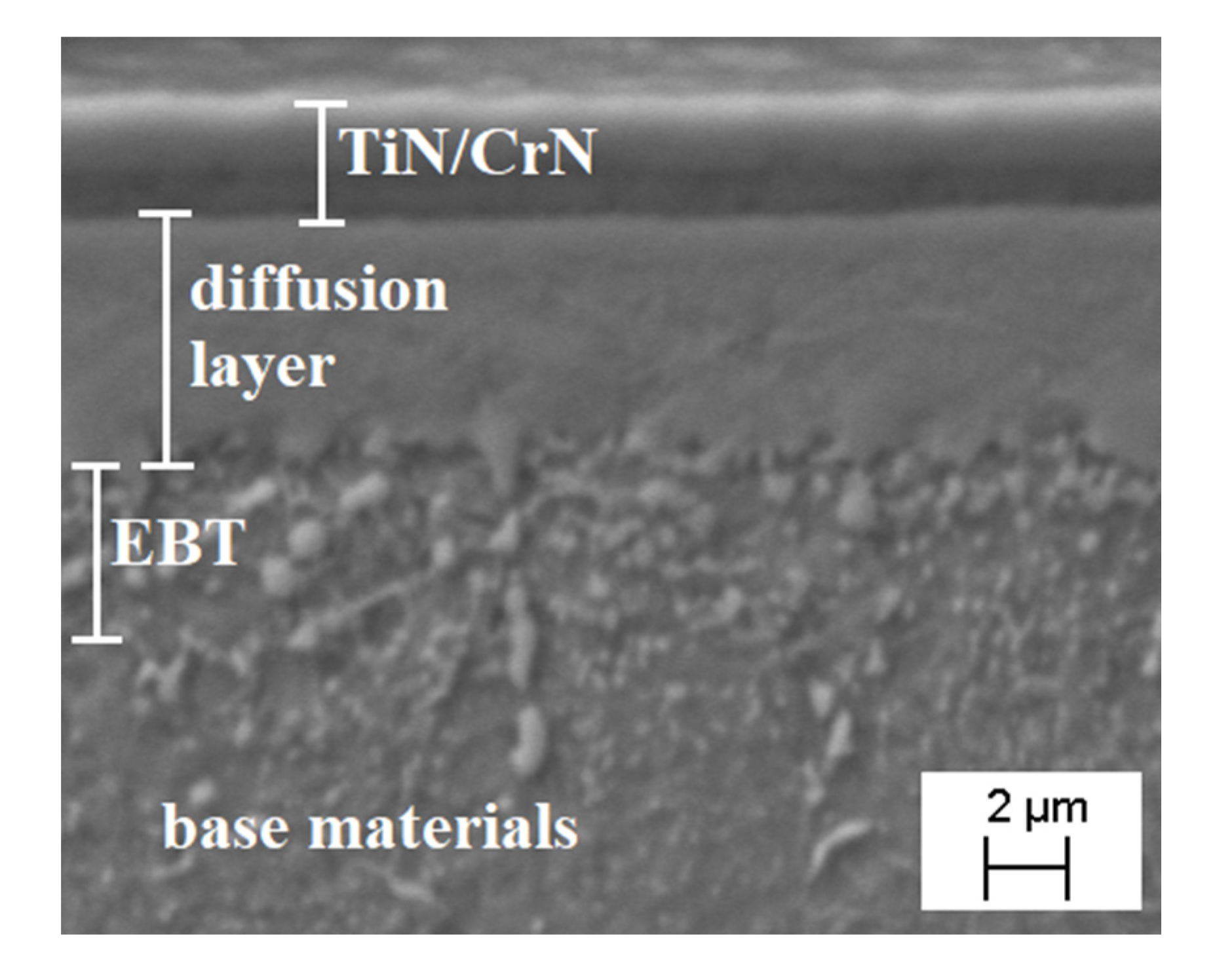
- Ormanova, M.; Dechev, D.; Bezdushnyi, R.; Petrov, P. Phase composition of multilayer system TiN/CrN deposited by DC magnetron sputtering. Bulg. Chem. Commun. 2017, 49, 98–102. [Google Scholar]
- Petrov, P.; Dechev, D.; Ivanov, N.; Hikov, T.; Valkov, S.; Nikolova, M.; Yankov, E.; Parshorov, S.; Bezdushnyi, R.; Andreeva, A. Study of the influence of electron beam treatment of Ti5Al4V substrate on the mechanical properties and surface topography of multilayer TiN/TiO2 coatings. Vacuum 2018, 154, 264–271. [Google Scholar] [CrossRef]
- Valkov, S.; Parshorov, S.; Andreeva, A.; Bezdushnyi, R.; Nikolova, M.; Dechev, D.; Ivanov, N.; Petrov, P. Influence of Electron Beam Treatment of Co–Cr Alloy on the Growing Mechanism, Surface Topography, and Mechanical Properties of Deposited TiN/TiO2 Coatings. Coatings 2019, 9, 513. [Google Scholar] [CrossRef] [Green Version]
- Grumbt, G.; Zenker, R.; Biermann, H.; Weigel, K.; Bewilogua, K.; Bräuer, G. Duplex Surface Treatment—Physical Vapor Deposition (PVD) and Subsequent Electron Beam Hardening (EBH). Adv. Eng. Mater. 2014, 16, 511–516. [Google Scholar] [CrossRef]
- Zaguliaev, D.; Gromov, V.; Rubannikova, Y.; Konovalov, S.; Ivanov, Y.; Romanov, D.; Semin, A. Structure and phase states modification of AL-11SI-2CU alloy processed by ion-plasma jet and pulsed electron beam. Surf. Coat. Technol. 2020, 383, 125246. [Google Scholar] [CrossRef]
- Zaguliaev, D.; Konovalov, S.; Ivanov, Y.; Gromov, V. Effect of electron-plasma alloying on structure and mechanical properties of Al-Si alloy. Appl. Surf. Sci. 2019, 498, 143767. [Google Scholar] [CrossRef]
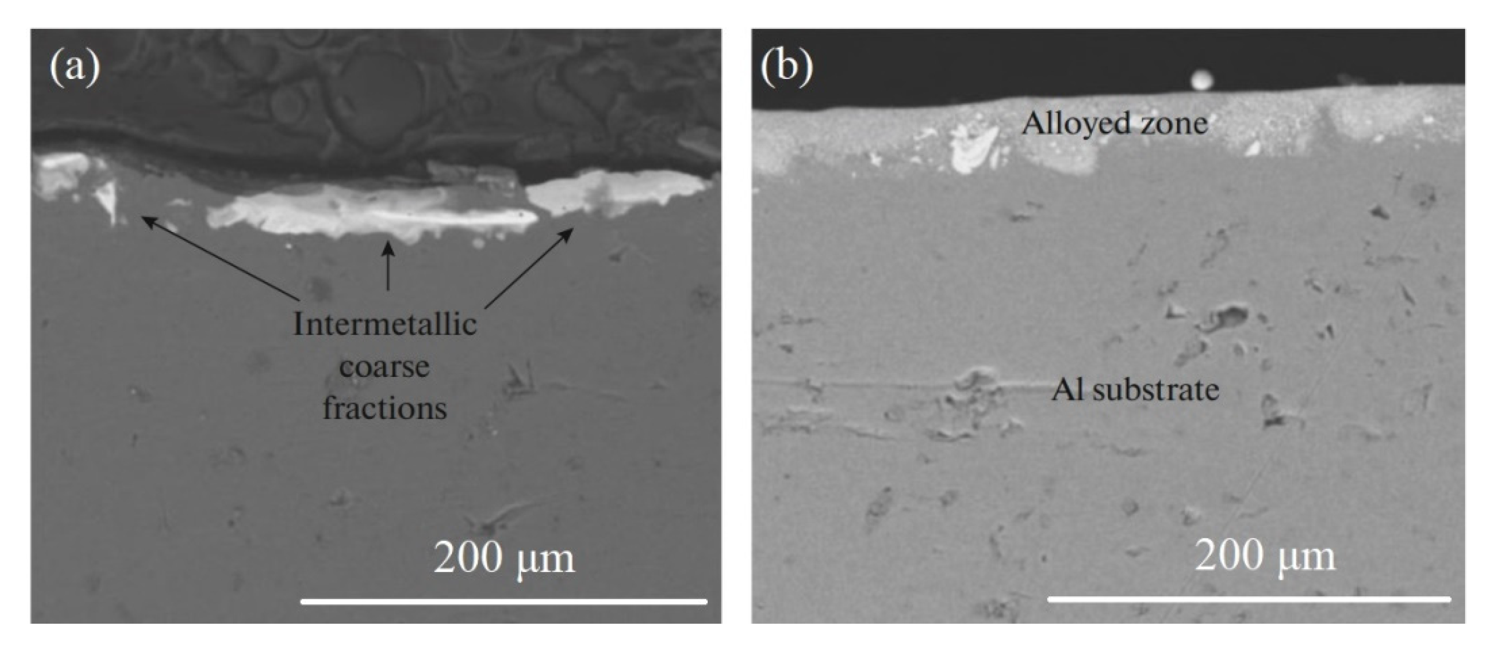
- Petrov, P. Electron beam surface remelting and alloying of aluminium alloys. Vacuum 1997, 48, 49–50. [Google Scholar] [CrossRef]
- Rotshtein, V.; Shulov, A. Surface Modification and Alloying of Aluminum and Titanium Alloys with Low-Energy, High-Current Electron Beams. J. Metall. 2011, 2011, 673685. [Google Scholar] [CrossRef] [Green Version]
- Rotshtein, V.; Markov, A.; Ivanov, Y. Surface treatment of materials with low-energy, high-current electron beam. In Materials Surface Processing by Directed Energy Techniques; Pauleau, Y., Ed.; Elsevier: Amsterdam, The Netherlands, 2006; pp. 205–240. [Google Scholar]
- Proskurovsky, D.; Rotshtein, V.; Ozur, G.; Ivanov, Y.; Markov, A. Physical foundations for surface treatment of materials with low energy, high current electron beams. Surf. Coat. Technol. 2000, 125, 49–56. [Google Scholar] [CrossRef]
- Petrov, P.; Dimitroff, D. Electron beam alloying of aluminum alloys. Vacuum 1993, 44, 857–861. [Google Scholar] [CrossRef]
- Petrov, P. Surface modification of aluminium alloys using hybrid treatment techniques. J. Phys. Conf. Ser. 2012, 356, 012035. [Google Scholar] [CrossRef]
- Zhang, C.; Lv, P.; Xia, H.; Yang, Z.; Konovalov, S.; Chen, X.; Guan, Q. The microstructure and properties of nanostructured Cr-Al alloying layer fabricated by high-current pulsed electron beam. Vacuum 2019, 167, 263–270. [Google Scholar] [CrossRef]
- Valkov, S.; Petrov, P.; Lazarova, R.; Bezdushnyi, R.; Dechev, D. Formation and characterization of Al–Ti–Nb alloys by electron-beam surface alloying. Appl. Surf. Sci. 2016, 389, 768–774. [Google Scholar] [CrossRef]
- Valkov, S.; Neov, D.; Bezdushnyi, R.; Beskrovnyi, A.; Kozlenko, D.; Petrov, P. Study of the Microstructure, Crystallographic Structure and Thermal Stability of Al–Ti–Nb Alloys Produced by Selective Electron Beam Alloying. J. Surf. Investig. X-ray Synchrotron Neutron Tech. 2018, 12, 436–441. [Google Scholar] [CrossRef]
- Chan, C.; Mazumder, J.; Chen, M. A two-dimensional transient model for convection in laser melted pool. Metall. Trans. A 1984, 15, 2175–2184. [Google Scholar] [CrossRef]
- Mei, X.; Fu, J.; Li, X.; Rotshtein, V.; Koval, N.; Ma, T. Surface alloying of Al films/Ti substrate based on high-current pulsed electron beams irradiation. Rare Metals 2014, 33, 155–160. [Google Scholar] [CrossRef]
- Rotshtein, V.; Ivanov, Y.; Kolubaeva, Y.; Mei, X.; Markov, A.; Naiden, E.; Ozur, G.; Oskomov, K.; Popov, S.; Pryadko, E.; et al. Synthesis of Ti3Al and TiAl based surface alloys by pulsed electron-beam melting of Al(film)/Ti(substrate) system. Tech. Phys. Lett. 2011, 37, 226–229. [Google Scholar] [CrossRef]
- Valkov, S.; Neov, D.; Luytov, D.; Petrov, P. Neutron diffraction of titanium aluminides formed by continuous electron-beam treatment. J. Phys. Conf. Ser. 2016, 700, 012034. [Google Scholar] [CrossRef]
- Batrakov, A.; Markov, A.; Ozur, G.; Proskurovsky, D.; Rotshtein, V. Surface alloying of metallic substrates with pre-deposited films through a pulsed electron-beam mixing. Eur. Phys. J. Appl. Phys. 2008, 43, 283–288. [Google Scholar] [CrossRef]
- Rotshtein, V.; Markov, A.; Shevchenko, N.; Reuther, H.; Oskomov, K.; Shulov, V. Surface doping of VT6 alloy with zirconium by pulsed electron-beam mixing of predeposited multilayer Zr/Ti film. Tech. Phys. Lett. 2008, 34, 891–894. [Google Scholar] [CrossRef]
- Zhang, L.; Peng, C.; Yao, X.; Guan, Q.; Lu, R. Surface alloying of Cr on Ti6Al4V alloy induced by high-current pulseelectron beam. Surf. Coat. Technol. 2019, 370, 288–297. [Google Scholar] [CrossRef]
- Valkov, S.; Bezdushnyi, R.; Petrov, P. Study of the influence of vanadium and niobium on the structure of Ti-Al-V and Ti-Al-Nb alloys formed by selective electron beam alloying. J. Phys. Conf. Ser. 2018, 992, 012053. [Google Scholar] [CrossRef]
- Valkov, S.; Bezdushnyi, R.; Petrov, P. Synthesis, structure and mechanical properties of Ti-Al-Nb coatings formed by electron beam additive technique. Vacuum 2018, 156, 140–145. [Google Scholar] [CrossRef]
- Rotshtein, V.; Ivanov, Y.; Markov, A.; Proskurovsky, D.; Karlik, K.; Oskomov, K.; Uglov, B.; Kuleshov, A.; Novitskaya, M.; Dub, S.; et al. Surface alloying of stainless steel 316 with copper usingpulsed electron-beam melting of film–substrate system. Surf. Coat. Technol. 2006, 200, 6378–6383. [Google Scholar] [CrossRef]
- Zhang, L.; Peng, C.; Shi, J.; Jin, Y.; Lu, R. Influence of high current pulsed electron beam on microstructure and properties of Ni–W alloy coatings. J. Alloys Compd. 2020, 858, 154460. [Google Scholar] [CrossRef]
- Zhang, L.; Peng, C.; Guan, J.; Lv, P.; Guan, Q. Nanocrystalline Cr-Ni Alloying Layer Induced by High-Current Pulsed Electron Beam. Nanomaterials 2019, 9, 74. [Google Scholar] [CrossRef] [Green Version]
- Zhang, L.; Peng, C.-T.; Shi, J.; Lu, R. Surface alloying of chromium/tungsten/stannum on pure nickel and theoretical analysis of strengthening mechanism. Appl. Surf. Sci. 2020, 532, 147477. [Google Scholar] [CrossRef]
- Zhang, C.; Lv, P.; Cai, J.; Peng, C.-T.; Jin, Y.; Guan, Q. The microstructure and properties of tungsten alloying layer on copper by high-current pulse electron beam. Appl. Surf. Sci. 2017, 422, 582–590. [Google Scholar] [CrossRef]
- Zhang, C.; Tian, N.; Li, L.; Yang, Z.; Lv, P.; Yunxue, J.; Zhu, H.; Guan, Q. The effect of high-current pulsed electron beam on phase formation and surface properties of chromium/copper system. Vacuum 2020, 174, 109222. [Google Scholar] [CrossRef]


© 2020 by the authors. Licensee MDPI, Basel, Switzerland. This article is an open access article distributed under the terms and conditions of the Creative Commons Attribution (CC BY) license (http://creativecommons.org/licenses/by/4.0/).
Share and Cite
Valkov, S.; Ormanova, M.; Petrov, P. Electron-Beam Surface Treatment of Metals and Alloys: Techniques and Trends. Metals 2020, 10, 1219. https://doi.org/10.3390/met10091219
Valkov S, Ormanova M, Petrov P. Electron-Beam Surface Treatment of Metals and Alloys: Techniques and Trends. Metals. 2020; 10(9):1219. https://doi.org/10.3390/met10091219
Chicago/Turabian StyleValkov, Stefan, Maria Ormanova, and Peter Petrov. 2020. "Electron-Beam Surface Treatment of Metals and Alloys: Techniques and Trends" Metals 10, no. 9: 1219. https://doi.org/10.3390/met10091219