Article

Resistive Switching Characteristics of ZnO-Based RRAM on Silicon Substrate

Division of Electronics and Electrical Engineering, Dongguk University, Seoul 04620, Korea
*
Author to whom correspondence should be addressed.
D.K. and J.S. is equally contributed in this work.
Metals 2021, 11(10), 1572; https://doi.org/10.3390/met11101572
Submission received: 29 August 2021 / Revised: 25 September 2021 / Accepted: 28 September 2021 / Published: 1 October 2021
(This article belongs to the Special Issue Metal Oxides Characterization for Emerging Memory Device Applications)

Abstract

:
In this work, we conducted the following analysis of Ni/ZnO (20 nm)/n-type Si RRAM device with three different compliance currents (CCs). We compared I–V curves, including set, reset voltages, and resistance of LRS, HRS states for each CCs. For an accurate comparison of each case, statistical analysis is presented. In each case, the average value and the relative standard deviation (RSD) of resistance are calculated to analyze the characteristics of the distribution. The best variability is observed at higher CC (5 mA). In addition, we validated the non-volatile properties of the device using the retention data for each of the CCs. Based on this comparison, we proposed the most appropriate CC of the device operation. Also, a pulse was applied to measure the current waveform and demonstrate the regular operation of the device. Finally, the resistance of LRS and HRS states was measured by pulse. We statistically compared the measured pulse data with the DC data.

1. Introduction

The demand to meet artificial intelligence (AI) technology for memory devices with high density and fast latency continues to intensify. NAND Flash memory, which is now widely used, has seen rapid growth in recent decades. However, it is inevitable that these conventional nonvolatile floating memories will reach technical and physical limits in the future [1]. In this situation, research of new memory devices to replace conventional memory formats is conducted. Resistive Random Access Memory (RRAM) is especially popular because it can be switched at high speed and handle computation and storage in a single device [2,3,4,5,6]. In addition, RRAM devices are also used in neuromorphic computing, which is studied to overcome the limitations of von Neumann computing [7,8,9,10,11]. A RRAM device consists of a metal-insulator-metal (MIM) structure. It has the characteristics of maintaining a low resistance state (LRS) at a specific voltage range and a high resistance state (HRS) at a different voltage range. The process of changing the state of a device to LRS is called ‘set,’ and the process of switching to HRS is called ‘reset.’ Set and reset processes are based on the phenomenon in which conducting filaments (CF) form or disappear inside the insulator between the top electrode (TE) and bottom electrode (BE). When applying excessively large voltages on the device, excessive CF can be formed. Excessive CF could not disappear in any case, and switching may not be possible. To prevent this phenomenon, CC should be applied to the device during the set process. If CC is set up before the set process, the current does not increase by more than a certain level, even if the voltage is raised after the device is changed to LRS. In contrast, the reset process implies a state transition from LRS to HRS, so CC is not required.
CC can not only limit the current after the set process but also change the overall characteristics of the current-voltage curve (I–V curve). If CC is large, a giant filament is formed in the process of being set, so a greater voltage is needed to destroy and reset this filament. In the same vein, the large CC makes the current value in the LRS state of the device even greater. The conduction mechanism and temperature dependence set in different CCs were studied in relation to CC [12]. In addition, the effects of different CCs for hopping conduction distance properties have been studied [13]. A compact SPICE model for circuit simulation, reflecting the characteristics of I-V curves that change with different CCs, was also studied [14].
Other important issues in RRAM devices are retention and endurance. Retention and endurance are important factors to demonstrate reliability as a non-volatile device. Moreover, understanding the retention and endurance degradation of RRAM as an artificial synapse device is critical for the development of neuromorphic computing [15]. Recently, optimum gate voltage for improving endurance while maintaining a high resistance ratio and the insensitivity of data retention of the HRS state to temperature and cycling-aging was studied [16]. Additionally, the endurance failure in a scaled RRAM device through the vacancy mobility gradation was studied, and the endurance and retention model of RRAM devices for deep learning simulations has also been studied [17].
In this paper, we explain the conduction mechanism of the Ni/ZnO (20 nm)/n-type Si device using a band diagram. Silicon bottom electrodes in a RRAM device could have several advantages. The resistive switching can be varied by impurity concentration in a silicon substrate [18]. Also, the silicon oxide acting as a tunnel barrier layer that improves the nonlinearity of I-V curves is made on a silicon substrate without any additional process [19]. ZnO RRAM, among a lot of metal oxide RRAMs, shows promising resistive switching properties for non-volatile memory [20] and neuromorphic applications [21]. However, the silicon bottom electrode in ZnO RRAM has been rarely discussed [22].
We compare the I-V curves, set, reset voltages, and cumulative probabilities of resistance measured through the Keithley equipment for each CC. Statistical figures are used for accurate comparison. Moreover, by analyzing the retention and endurance data for each CC, we propose the most appropriate CC for the operation of the device. Also, the pulse data is measured based on the experimentally obtained set and reset voltages to analyze the operation of the device. The potential as a logic-in-memory application memristor has also been verified through this pulse data. Finally, the resistance value of LRS and HRS measured in pulses, in addition to DC data, are compared. We effectively demonstrate the operational characteristics, reliability, and potential of Ni/ZnO/Si RRAM devices.

2. Materials and Methods

Ni/ZnO/Si devices were prepared through the following process. A-200-nm thick n-type Si bottom electrode (doping concentration >1021 cm−3 was deposited on SiO2/Si wafer by low-pressure chemical vapor deposition (LPCVD) by reacting SiH4 and PH3. A 13-nm-thick ZnO layer was deposited via pulsed DC sputtering on an n-type Si. A Zn source-target was used to react with oxygen for ZnO film deposition in which the 1 mTorr of sputtering pressure and 0.2 kW of sputtering power. Ar (6 sccm) and O2 (14 sccm) gases were passed through the chamber during deposition. Ni top electrode was deposited by e-beam evaporator via shadow mask containing a circular pattern with a diameter of 100 μm. A Keithley 4200-SCS semiconductor parameter analyzer (SPA) and a 4225-PMU pulse measurement unit in the probe station were used to measure electrical characteristics using DC sweep mode and transient characteristics. A bias was applied to the Ni top electrode and the Si bottom electrode was grounded.

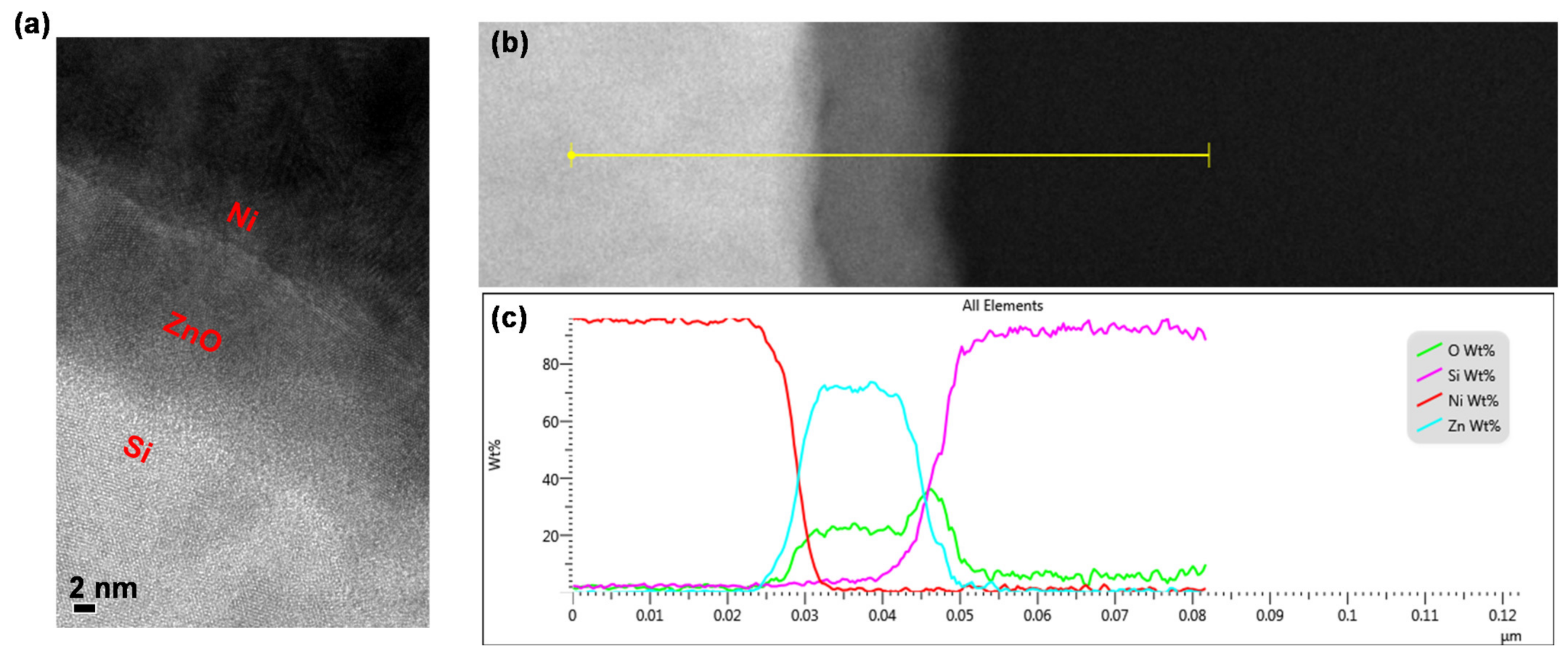
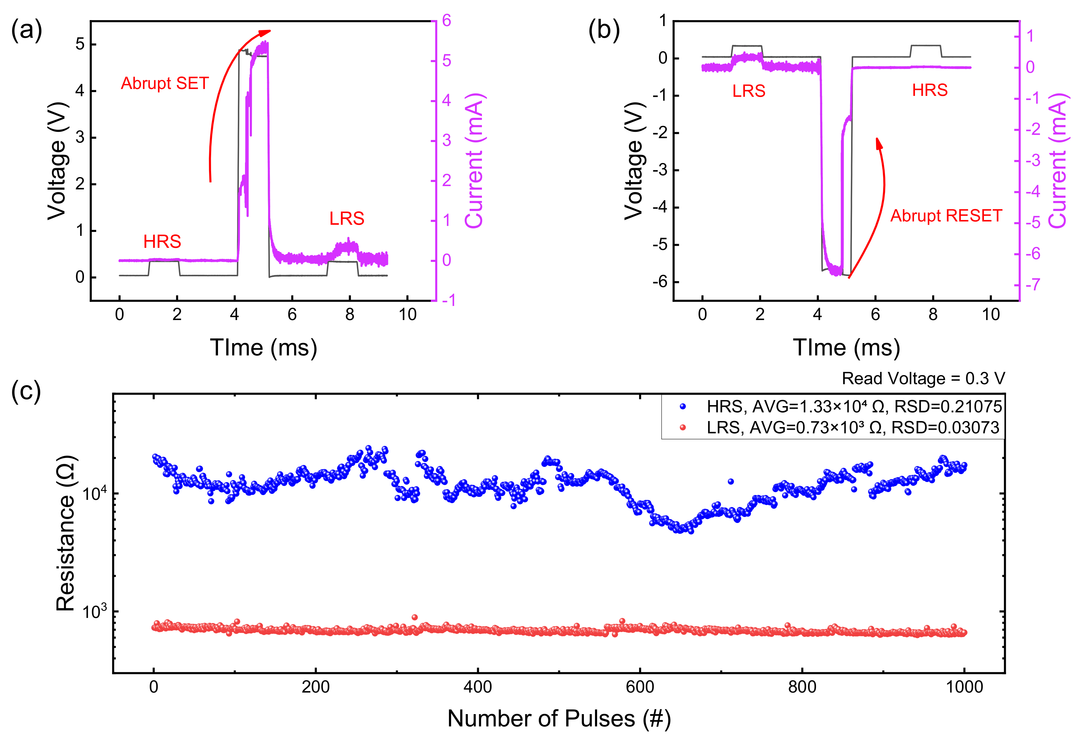
3. Results and Discussion

Figure 1a shows a high-resolution transmission electron microscope (TEM) image. The thickness of the amorphous ZnO layer is about 13 nm. Polysilicon Si deposited by LPCVD is confirmed as the bottom electrode for the memory device. Also, a thin band-like layer between the ZnO layer and the Si electrode is observed. Native oxide could be formed before the ZnO deposition. Scanning transmission electron microscopy (STEM) and an energy-dispersive X-ray spectroscopy (EDS) line scan were used to confirm the element of each layer in Figure 1b,c. The SiOx layer between ZnO and Si layers is clearly observed in the EDS line scan in Figure 1c.
The conduction mechanism of the Ni/ZnO/Si device is presented using schematics in Figure 2a–e. When the TE is applied with a positive voltage, the oxide ions move towards the top. CF is grown towards the top by the movement of oxygen vacancies. The opposite polarity of voltage should be applied to remove the CF that connects TE and BE in bipolar resistive switching. The reset process is carried out as opposed to the set process. Also, the energy band diagram of the device is shown in Figure 2f–h. The essential parameters of the materials used in the device are attached to Table 1 [23,24,25]. It is illustrated in Ni/ZnO/Si to match the stack of devices, and the SiO₂ layer, a native oxide film, is also considered on the interface of ZnO and Si. The electron moves from the silicon substrate during the set process, and, in the end, the conducting filament is formed in the dielectrics. On the other hand, the electron moves from the Ni electrode to dielectrics under the reset process. Moreover, a possible conduction mechanism is space-charge limited current (SCLC) in Supplementary Materials (Figure S1).
The measured I-V characteristics of the devices with different CCs (0.5 mA, 1 mA, and 5 mA) are shown in Figure 3a–c. Each case is the result of a DC sweep of 100 cycles. For each I–V curve, the voltage just before the current level is increased from HRS to LRS is defined as set voltage, and the voltage just before the LRS fall from LRS to HRS is defined as reset voltage. One hundred cycles of set voltages and reset voltages are investigated for each CC. To find out the spectrum of the operating voltage, a box chart is presented in Figure 3d. When CC is 0.5 mA, the spectrums of set and reset voltages are very wide, and the current in LRS and HRS is also highly variable. Variation of the current and set, reset voltages is also significant when CC = 1 mA. However, if CC is 5 mA, set and reset occur at a relatively narrow range of voltages, and the current in the LRS and HRS states is relatively low in terms of variation. I–V curves and a box chart show that the greater CC, the greater the reset voltage. A larger reset voltage is required to reset the device again because the strong filament is formed when CC is set to be large. Therefore, when comparing each set voltage of different CCs, there is no significant difference in the value of the voltage, and only the variation decreases as CC increases. However, when comparing reset voltages, a large CC needs a much higher reset voltage. We analyzed the resistance to find out the current variability in each state. Figure 3e,f presents the cumulative probability of resistance values with each CC. For example, for a blue-colored graph of CC = 5 mA, the cumulative probability is consistently located at around 5.9 kΩ with some points of the tailed bit. An RSD, as well as the average of the resistance values, was calculated. HRS in Figure 3e shows that the smaller CC, the greater the resistance. While CC = 5 mA and CC = 0.5 mA remain relatively constant, CC = 1 mA shows large variation. In Figure 3f, CC = 5 mA remains almost constant even though some tail bit is spread. As the CC increases, the variation tends to decrease, which means stable resistive switching is attained in higher CC.
The results of measuring the resistance of HRS and LRS during 100 cycles are shown in the endurance cycle in Figure 4a–c. First, HRS at CC = 5 mA shows the most stable and constant value. CC = 0.5 mA shows moderate uniformity, while CC = 1 mA shows very severe variation, including switching error. These results can also be found in the aforementioned Figure 3e. In the case of CC = 1 mA, the values are not consistent vertically. The rest of the CCs have relatively consistent values. In addition, for the LRS state, the most uniform data is also shown at CC = 5 mA. CC = 1 mA also remains relatively stable, but CC = 0.5 mA has a significant variation. This result can also be found in the aforementioned Figure 3f. In the cumulative probability data of LRS, CC = 5 mA shows the best uniformity while CC = 0.5 mA presents very severe non-uniformity. In addition to endurance, measuring the device’s retention is one of the most important issues in terms of reliability. This is shown in Figure 4d–f. In the case of retention, 0.3 V was applied 1000 times with 10 s intervals, so it took 10,000 s for each case. LRS retention data of all three different CCs converges on ideal values. However, in the case of HRS retention, the resistance of the device was slightly increased due to stress, but it shows variability within acceptable ranges. Three different CCs can be judged to satisfy the operational reliability in terms of preserving data.
Additionally, we examined whether the device works ideally for set and reset processes when a pulse is applied. The pulse with a very low voltage cannot change the device’s state, but the present state of the device can be checked without disturbance. The transition of the state of the device is measured for set and reset processes in Figure 5a,b. Three serial pulses with peak values of 0.3 V, 4.8 V, and 0.3 V are applied to the device, which is in the HRS state in Figure 5a. Since the device is initially set to “off”, the current of the first pulse is of a very low measure. The state of the device is switched because the second pulse has a large enough peak voltage to make the device switch to the LRS state. The third pulse is measured at a high level of current, reflecting the change of the device state, and the current follows the waveform of the pulse. The peak voltage of the third pulse is 0.3 V, so the current of the high level flowing at this moment corresponds to the current range at 0.3 V in the I-V curve presented earlier. In the same vein, serial pulses of 0.3 V, −5.8 V, and 0.3 V are applied to the device, which is in the LRS state at first for the reset process in Figure 5b. Initially, the device is set to “on”, so the high level of current is measured, and the current follows the waveform of the pulse. The peak voltage of this pulse is 0.3 V, so the current at this time corresponds to the current range at 0.3 V on the I-V curve. The state of the device was switched because the second pulse has enough peak voltage to lead the device to the HRS state. The third pulse is measured at a very low-level current, reflecting the change of the device state. This device achieves an ideal state transition when the pulse is applied, implying the potential as a logic-in-memory application. RRAM devices with logic-in-memory ability have great potential for constructing post-von-Neumann computing [26]. However, since conducting filaments are activated randomly inside the RRAM devices, there is a disadvantage of showing poor switching uniformity. Therefore, this is a limitation in that it is difficult to implement logic-in-memory requirements. In this study, we expected this result to be of significant help to satisfy the logic-in-memory requirement by suggesting the CC that the device can operate at most credibly. The comprehensive analysis shows that the Ni/ZnO (13 nm)/n-type Si device can operate most reliably with 5 mA. At CC = 5 mA, the ranges of the set, reset voltages are the least variable. Also, the resistance of HRS and LRS shows the most uniform values within 100 cycles. Retention data is also measured credibly, and the device is operated smoothly when the pulse is applied.
Finally, we present the resistance of LRS and HRS measured by pulses in Figure 5c. All of the pulses have an interval of 0.88 ms, and the interval between pulses is also 0.88 ms. The read voltage is selected as 0.3 V. The results of applying 1000 pulses are shown in Figure 5c, but only the initial 100 pulses are considered to calculate the average and the relative standard deviation values of each state. When comparing statistical values of the pulses with the results measured in DC, the number of pulses is limited to prevent the effect of measurement frequencies. According to the results measured in pulses, the average value of resistance at the HRS state is calculated to be 1.33 × 10⁴ Ω, and the relative standard deviation value is 0.21. These two values are most similar to the results of CC = 1 mA, measured in DC, and show a relatively severe deviation. On the other hand, the average value of resistance is calculated as 0.73 × 10³ Ω, and the relative standard deviation value is 0.03. These two values are most similar to the results of CC = 5 mA when measured in DC, with very little deviation. In conclusion, it can be seen that the data measured in pulses remains stable at LRS while the deviation is severe at HRS.

4. Conclusions

In this study, the conduction mechanism and energy band diagram of the Ni/ZnO (20 nm)/n-type Si device was described. Three different CCs were set to represent each I-V curve. I-V curves were analyzed to investigate operating voltage ranges for each CC. Set voltages showed no significant difference in all three cases, with variation being the only difference. The absolute values of reset voltages increase as CC increases. The operating voltage variation is smallest at CC = 5 mA. When the device is in the HRS and LRS state, we represent the cumulative probability of resistance for each CC at 0.3 V. In both cases, CC = 5 mA has the most constant value. Similar distributions can be seen through the endurance data. In HRS, the variation is particularly severe at CC = 1 mA, and in LRS, the variation is most severe at CC = 0.5 mA. If CC = 5 mA, both HRS and LRS are stable. Retention data for each CC was measured to determine the conservation of data. 0.3 V is applied 1000 times at 10-s intervals, and all three different CCs preserved data within the normal range in both LRS and HRS. As a result, the most appropriate CC for the reliable operation of this device is analyzed at 5 mA. In addition, a pulse train is applied to the device to examine its operating ability. There is no state change at a low-leveled pulse, and the current change occurred abruptly at a pulse that is large enough to lead set or reset. Resistance of the LRS, HRS state measured through pulses was also presented. According to the pulse data, the HRS state showed a significant deviation similar to HRS at CC = 1 mA in DC. However, at the LRS state in pulses, the variation was identical to the results of LRS at CC = 5 mA in DC.

Supplementary Materials

The following are available online at https://www.mdpi.com/article/10.3390/met11101572/s1, Figure S1: SCLC fitting of Ni/ZnO/Si device.

Author Contributions

J.S. conducted the electrical measurements, and D.K. wrote the manuscript; S.K. designed the experiment and supervised the study. All authors have read and agreed to the published version of the manuscript.

Funding

This work was supported in part by a National Research Foundation of Korea (NRF) grant funded by Ministry of Science and ICT (2021R1C1C1004422).

Institutional Review Board Statement

Not applicable.

Informed Consent Statement

Not applicable.

Data Availability Statement

Not applicable.

Conflicts of Interest

The authors declare no conflict of interest.

References

  1. Lee, G.; Hwang, S.; Yu, J.; Kim, H. Architecture and Process Integration Overview of 3D NAND Flash Technologies. Appl. Sci. 2021, 11, 6703. [Google Scholar] [CrossRef]
  2. Lanza, M.; Wong, H.-S.P.; Pop, E.; Ielmini, D.; Strukov, D.; Regan, B.C.; Larcher, L.; Villena, M.A.; Yang, J.J.; Goux, L.; et al. Recommended Methods to Study Resistive Switching Devices. Adv. Electron. Mater. 2018, 5, 1800143. [Google Scholar] [CrossRef] [Green Version]
  3. Linn, E.C.; Rosezin, R.D.; Kügeler, C.; Waser, R. Complementary resistive switches for passive nanocrossbar memories. Nat. Mater. 2010, 9, 403–406. [Google Scholar] [CrossRef]
  4. Mikhaylov, A.; Belov, A.; Korolev, D.; Antonov, I.; Kotomina, V.; Kotina, A.; Gryaznov, E.; Sharapov, A.; Koryazhkina, M.; Kryukov, R.; et al. Multilayer Metal-Oxide Memristive Device with Stabilized Resistive Switching. Adv. Mater. Technol. 2019, 5. [Google Scholar] [CrossRef]
  5. Ryu, H.; Kim, S. Self-Rectifying Resistive Switching and Short-Term Memory Characteristics in Pt/HfO2/TaOx/TiN Artificial Synaptic Device. Nanomaterials 2020, 10, 2159. [Google Scholar] [CrossRef]
  6. Kim, S.; Jung, S.; Kim, M.-H.; Chen, Y.-C.; Chang, Y.-F.; Ryoo, K.-C.; Cho, S.; Lee, J.-H.; Park, B.-G. Scaling Effect on Silicon Nitride Memristor with Highly Doped Si Substrate. Small 2018, 14, e1704062. [Google Scholar] [CrossRef] [PubMed]
  7. Ryu, H.; Kim, S. Pseudo-Interface Switching of a Two-Terminal TaOx/HfO2 Synaptic Device for Neuromorphic Applications. Nanomaterials 2020, 10, 1550. [Google Scholar] [CrossRef]
  8. Ryu, H.; Choi, J.; Kim, S. Voltage Amplitude-Controlled Synaptic Plasticity from Complementary Resistive Switching in Alloying HfOx with AlOx-Based RRAM. Metals 2020, 10, 1410. [Google Scholar] [CrossRef]
  9. Ohno, T.; Hasegawa, T.; Tsuruoka, T.; Terabe, K.; Gimzewski, J.; Aono, M. Short-term plasticity and long-term potentiation mimicked in single inorganic synapses. Nat. Mater. 2011, 10, 591–595. [Google Scholar] [CrossRef]
  10. Su, Y.; Chang, K.-C.; Chang, T.-C.; Tsai, T.-M.; Zhang, R.; Lou, J.C.; Chen, J.-H.; Young, T.-F.; Chen, K.-H.; Tseng, B.-H.; et al. Characteristics of hafnium oxide resistance random access memory with different setting compliance current. Appl. Phys. Lett. 2013, 103, 163502. [Google Scholar] [CrossRef] [Green Version]
  11. Ryu, H.; Kim, S. Gradually Tunable Conductance in TiO2/Al2O3 Bilayer Resistors for Synaptic Device. Metals 2021, 11, 440. [Google Scholar] [CrossRef]
  12. Ismail, M.; Abbas, H.; Choi, C.; Kim, S. Controllable analog resistive switching and synaptic characteristics in ZrO2/ZTO bilayer memristive device for neuromorphic systems. Appl. Surf. Sci. 2020, 529, 147107. [Google Scholar] [CrossRef]
  13. Chen, H.-K.; Chang, K.-C.; Chang, T.-C.; Tsai, T.-M.; Liao, K.-H.; Syu, Y.-E.; Sze, S.M. Effect of different constant compliance current for hopping conduction distance properties of the Sn:SiOx thin film RRAM devices. Appl. Phys. A 2016, 122, 228. [Google Scholar] [CrossRef]
  14. Yu, S.; Wong, H.S.P. Compact Modeling of Conducting-Bridge Random-Access Memory (CBRAM). IEEE Trans. Electron Devices 2011, 58, 1352–1360. [Google Scholar]
  15. Zhao, M.; Gao, B.; Xi, Y.; Xu, F.; Wu, H.; Qian, H. Endurance and Retention Degradation of Intermediate Levels in Filamentary Analog RRAM. IEEE J. Electron. Devices Soc. 2019, 7, 1239–1247. [Google Scholar] [CrossRef]
  16. Chen, Y.-C.; Lin, C.-C.; Hu, S.-T.; Lin, C.-Y.; Fowler, B.; Lee, J. A Novel Resistive Switching Identification Method through Relaxation Characteristics for Sneak-path-constrained Selectorless RRAM application. Sci. Rep. 2019, 9, 12420. [Google Scholar] [CrossRef] [Green Version]
  17. Lammie, C.; Azghadi, M.R.; Ielmini, D. Empirical metal-oxide RRAM device endurance and retention model for deep learning simulations. Semicond. Sci. Technol. 2021, 36, 065003. [Google Scholar] [CrossRef]
  18. Kim, S.; Chang, Y.F.; Park, B.G. Understanding rectifying and nonlinear bipolar resistive switching characteristics in Ni/SiNx/p-Si memory devices. RSC Adv. 2017, 7, 17882. [Google Scholar] [CrossRef] [Green Version]
  19. Kim, S.; Jung, S.; Kim, M.-H.; Cho, S.; Park, B.-G. Resistive switching characteristics of Si3N4-based resistive-switching random-access memory cell with tunnel barrier for high density integration and low-power applications. Appl. Phys. Lett. 2015, 106, 212106. [Google Scholar] [CrossRef]
  20. Simanjuntak, F.M.; Ohno, T.; Samukawa, S. Influence of rf sputter power on ZnO film characteristics for transparent memristor devices. AIP Adv. 2019, 9, 105216. [Google Scholar] [CrossRef] [Green Version]
  21. Simanjuntak, F.M.; Ohno, T.; Samukawa, S. Film-Nanostructure-Controlled Inerasable-to-Erasable Switching Transition in ZnO-Based Transparent Memristor Devices: Sputtering-Pressure Dependency. ACS Appl. Electron. Mater. 2019, 11, 2184–2189. [Google Scholar] [CrossRef]
  22. Simanjuntak, F.M.; Panda, D.; Wei, K.H.; Tseng, T.Y. Status and Prospects of ZnO-Based Resistive Switching Memory Devices. Nanoscale Res. Lett. 2016, 11, 368. [Google Scholar] [CrossRef] [Green Version]
  23. Shimura, K.; Yoshida, H. Heterogeneous photocatalytic hydrogen production from water and biomass derivatives. Energy Environ. Sci. 2011, 4, 2467–2481. [Google Scholar] [CrossRef]
  24. Chizhov, A.S.; Rumyantseva, M.N.; Vasilieva, R.B.; Filatova, D.F.; Drozdov, K.A.; Krylov, I.V.; Marchevsky, A.V.; Karakulina, O.M.; Abakumov, A.M.; Gaskov, A. Visible light activation of room temperature NO2 gas sensors based on ZnO, SnO2 and In2O3 sensitized with CdSe quantum dots. Thin Solid Film. 2016, 11, 253–262. [Google Scholar] [CrossRef]
  25. Fujimura, N.; Ohta, A.; Makihara, K.; Miyazaki, S. Evaluation of valence band top and electron affinity of SiO2 and Si-based semiconductors using X-ray photoelectron spectroscopy. Jpn. J. Appl. Phys. 2016, 55, 08PC06. [Google Scholar] [CrossRef]
  26. Gao, S.; Liu, G.; Chen, Q.; Xue, W.; Yang, H.; Shang, J.; Chen, B.; Zeng, F.; Song, C.; Pan, F.; et al. Improving Unipolar Resistive Switching Uniformity with Cone-Shaped Conducting Filaments and Its Logic-In-Memory Application. ACS Appl. Mater. Interfaces 2018, 10, 6453–6462. [Google Scholar] [CrossRef] [PubMed]
Figure 1. (a) TEM image, (b) STEM image, (c) EDS line scan of Ni/ZnO/Si memory device.
Metals 11 01572 g001
Figure 2. Schematics of possible conducting filament model. (a) initial state. (b) set process. (c) LRS. (d) reset process. (e) HRS. Simple energy band diagram. (f) Work function and energy gap of each layer. (g) set process. (h) reset process.
Metals 11 01572 g002
Figure 3. (a) I-V curves of CC = 0.5 mA, (b) CC = 1 mA and (c) CC = 5 mA. (d) Box chart of set voltages and reset voltages of each CCs. Cumulative probability of resistance of (e) HRS and (f) LRS.
Metals 11 01572 g003
Figure 4. Endurance data of (a) CC = 0.5 mA, (b) CC = 1 mA and (c) CC = 5 mA. Retention data of (d) CC = 0.5 mA, (e) CC = 1 mA and (f) CC = 5 mA.
Metals 11 01572 g004
Figure 5. (a) Serial pulses to measure current level (0.3 V, 4.8 V, 0.3 V to lead set) and (b) (0.3 V, −5.8 V, 0.3 V to lead reset). (c) Resistance of HRS and LRS measured through pulses.
Metals 11 01572 g005
Table 1. Material parameters for Ni/ZnO/SiO2/Si structure.
MatrialWork Function (eV)Electron Affinity (eV)Band Gap (eV)
Ni5.15--
ZnO-4.63.3
SiO₂-0.99.0
Si-4.031.12
Publisher’s Note: MDPI stays neutral with regard to jurisdictional claims in published maps and institutional affiliations.

