Abstract
High-current pulsed electron-beam (PEB) treatment was applied as a surface finishing procedure for Ti–35Nb–7Zr–5Ta (TNZT) alloy produced by electron beam melting (EBM). According to the XRD results the TNZT alloy samples before and after the PEB treatment have shown mainly the single body-centered cubic (bcc) β-phase microstructures. The crystallite size, dislocation density, and microstrain remain unchanged after the PEB treatment. The investigation of the texture coefficient at the different grazing angle revealed the evolution of the crystallite orientations at the re-melted zone formed at the top of the bulk samples after the PEB treatment. The top-view SEM micrographs of the TNZT samples treated by PEB exhibited the bcc β-phase grains with an average size of ~85 μm. TEM analysis of as-manufactured TNZT alloy revealed the presence of the equiaxed β-grains with the fine dispersion of nanocrystalline α and NbTi4 phases together with β-Ti twins. Meanwhile, the β phase regions free of α phase precipitation are observed in the microstructure after the PEB irradiation. Nanoindentation tests revealed that the surface mechanical properties of the melted zone were slightly improved. However, the elastic modulus and microhardness in the heat-affected zone and the deeper regions of the sample were not changed after the treatment. Moreover, the TNZT alloy in the bulk region manufactured by EBM displayed no significant change in the corrosion resistance after the PEB treatment. Hence, it can be concluded that the PEB irradiation is a viable approach to improve the surface topography of EBM-manufactured TNZT alloy, while the most important mechanical parameters remain unchanged.
1. Introduction
In current biomaterial research, the development of new materials with improved physicochemical properties and enhanced functional performance characteristics is attracting significant attention. The design and manufacture of novel titanium (Ti)-based alloys for biomedical applications in load-bearing areas, such as hip or knee implants, is of specific interest for several reasons. Firstly, a polycrystalline α+β TiAl6V4 wt% alloy, which is widely used in biomedicine, suffers from two main disadvantages. It has a high risk of the stress-shielding induced by the difference in Young modulus between the replacement material (E ~110 GPa) and natural human bones (20–30 GPa) and incites. Moreover, it contains aluminum and vanadium elements that can cause cytotoxicity. Secondly, there is a strong increase in the need for these materials, due to the ongoing aging of the population and increasing mobility of the elderly [1,2]. For instance, Krutz et al. [3] have predicted growth of 174% (572,000 procedures) for the total number of hip arthroplasties and 673% (3.48 million procedures) for knee replacements from 2005 to 2030.
The main requirements for the development of novel Ti-based alloys for the manufacturing of load-bearing bone implants are high strength, excellent chemical stability in corrosive media, as well as a relatively low modulus of elasticity and sufficiently good plasticity, low cytotoxicity, and lowest risks for allergic reactions [4,5].
To overcome the above-mentioned issues, the second-generation materials based on Ti alloys was proposed, which occur in the following crystal structures or their combinations: the hcp α-phase (P63/mmc (No. 194)) and bcc β-phase (No. 229). Thus, three main target classes of Ti-based alloys can be defined as α, pseudo α, (α + β), and β. For pure Ti, the transition temperature from α to β-phase is ~882 °C. Several elements can affect the transition temperature value, among which are so-called α-stabilizers (e.g., O, Al, La) and β-stabilizers (e.g., Mo, Nb, and Ta).
Most of the current research is focused on the metastable β-Ti alloys, as they possess intrinsically lower modulus and higher strength compared to α- or α+β Ti-based alloys.
One of the most promising of these alloys is β Ti–35Nb–7Zr–5Ta wt% (TNZT) alloy, popularly known as “gum metal” [6], which possesses one of the lowest elastic moduli among the β-Ti family (at ~48…65 GPa), and contains no cytotoxic elements [7]. Investigations demonstrated that this alloy has excellent corrosion resistance and biocompatibility [6]. The most perspective method to fabricate orthopedic implants is additive manufacturing [8]. The most widely used material for the production of the orthopedic implants by additive manufacturing is two-phase α+β titanium alloy Ti–6Al–4V. The TNZT alloy was obtained by various additive methods earlier [9]. However, no reports have yet been devoted to the study of the EMB manufacturing of TNZT alloy.
As-built additive manufactured metal parts reveal the high surface roughness, the presence of porosities due to the lack of fusion, and unmelted or semi-melted powder particles attached to the surface [10]. However, roughness plays an important role in the mechanical properties, such as ductility, ultimate tensile strength, yield strength, and the fatigue strength of Ti6Al4V parts fabricated by EBM due to the fatigue crack initiation in the metals, which occurred at the roughened surfaces [11]. The surface finish of EBM-fabricated materials is also required due to the requirements of faster integration. To achieve a better surface finish, additional post-processing is utilized.
Surface modifying of this alloy is a viable strategy for the improvement of wear/corrosion resistance and biocompatibility by tailoring the surface composition, microstructure, and mechanical properties [12,13]. Nowadays, there are a lot of ways to do the surface modification of Ti alloys, such as gas nitriding [14], laser nitriding [15], thermal oxidation [16], TiN coatings [17], laser irradiation [18], and electron beam surface re-melting or alloying [19,20], etc.
Evaluations of the mechanical properties and surface microstructure of the PEB treated metals for biomedical applications have also shown promising results. In recent years, surface treatment with high current PEB has demonstrated a significant increase in dynamic strength and resistance to wear and corrosion [20,21,22,23].
To our knowledge, the investigation of the physico-mechanical properties in combination with corrosion resistance test using additively manufactured TNZT samples treated by PEB were, to date, not performed. Moreover, to our best knowledge, TNZT alloy was firstly treated by impulse electron beam in the present study. Therefore, the intention of this study is to demonstrate the positive effect of the PEB treatment of TNZT samples on wear/corrosion resistance. The samples are characterized by means of chemical analysis, XRD, SEM, and TEM. Finally, the indentation test and roughness measurement results are discussed.
2. Materials and Methods
2.1. EBM Fabrication and PEB Treatment of TNZT Samples
Prealloyed spherical powder of Ti-35 wt% Nb-7 wt% Zr-5 wt% Ta (TNZT) produced by Tosoh SMD Inc. (Grove City, PA, USA) was used as a precursor material. The details of production, characteristics, and properties of prealloyed TNZT powder are described elsewhere [24].
Several attempts for manufacturing bulk specimens were made based on a trial-and-error approach. Powder with a wide grain size distribution was used (as received from Tosh SMD Inc.), however, other EBM manufacturing parameters were varied to escape manufacturing defects. Thus, layer thickness was varied from 200 µm to 100 µm, beam current was varied from 11 to 3 mA, beam velocity was varied from 2409 to 407 mm/s, and line offset was varied from 0.1 to 0.07 mm. Thick layer and excessively large beam current and velocity lead to layer delamination and surface swelling (Table 1). Full details of the equipment used in the Arcam EBM® process and process parameter settings are described elsewhere [25].

Table 1.
EBM Manufacturing Properties.
The evaluation of the average applied energy per area and volume of a material during the melting of a layer can be done by calculating the area energy (EA) and the volumetric energy density (Eν) as follows:
where v, P, U, I, h, and t are the beam velocity, beam power, beam accelerating voltage, beam current, line offset (spacing between hatch lines), and thickness of the layer, respectively. To control thermal conditions of additive manufacturing an actual temperature on the bottom of the start plate is used and is kept stable during the manufacturing process through the implementation of additional heating stages into the common for EBM presintering-(heating)-melting-(heating)-powder deposition process flow. Due to the small sample sizes s and melting of layers directly from the start plate, the temperature taken at the bottom of start plate well represents the temperature of the samples. Specimens with area energy of 4.4 J/mm2 were chosen for further investigations as they had the best morphology, kept their integrity, and had the lowest amount of manufacturing defects.
The surface of the Ti alloy was treated by a PEB. The treatment of as-manufactured TNZT alloy surface was carried out with a PEB generator “SOLO” at the Institute of High Current Electronics SB RAS (Tomsk, Russia). The process parameters of the irradiation were as follows: the number of pulses was 10, the duration of the electron beam pulse was 200 μs, and the electron beam energy density was 20 J cm−2. The beam was wide enough to cover all the treated areas at once. The image of the electron beam treated surfaces obtained in the study is shown in Figure 1. It is clearly seen that finished surfaces do not have partially melted or even unmelted powder particles.
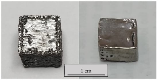
Figure 1.
Image of the untreated (left) and PEB treated (right) surfaces modified with area energy of 4.4 J/mm2 from the study.
2.2. Characterization of the Samples
The morphology and elemental composition of the as-manufactured and PEB treated TNZT alloy were studied by means of scanning electron microscopy (SEM, Quanta 200D and JSM-7000, JEOL, Tokyo, Japan) equipped with the energy-dispersive X-ray spectroscope (EDXS, Quanta 200D).
Surface roughness was evaluated by profilometry using a Hommel tester t1000. The average roughness (Ra), the five-wheel profile valleys within the length (Rz), and the largest profile height (Rmax) were measured. The microstructure was investigated using a transmission electron microscope (TEM) (JEOL JEM 2500SE, JEOL Ltd., Tokyo, Japan) operated at 200 kV. The phase composition and the structure of the TNZT powder were studied by X-ray diffraction (XRD-7000, Shimadzu, Japan) using CuKα radiation (λ = 0.154 nm) in Bragg–Brentano mode and a 2 theta range from 10° to 90° with a scan speed of 2.0°/min, sampling pitch of 0.02°, preset time of 1.0 s at 30 kV and 30 mA.
The TNZT samples were analyzed by X-ray diffraction technique by a SmartLab system (Rigaku, Japan) using a 9 kW rotating anode with CuKα radiation source (λ = 1.5418 Ǻ). The diffractometer was operating in a Parallel Beam configuration (with Parabolic multi-layer mirror) and in a high-resolution mode using a Ge (220) × 2 monochromator. The HyPix-3000 detector was used for data acquisition. The measurements were obtained at a grazing angle of 3–15 deg., with a speed of 1 deg./s, in 2 theta range of 10–90 deg. Grazing incidence X-ray diffraction (GIXRD) analysis was chosen for revealing the phase distribution in the uppermost surface layer of the PEB treated samples.
Metkon Forcipol 2V, Metkon Instruments Inc. polishing/grinding machine was used to prepare specimens’ surfaces for further investigation. The specimens were initially cut across to and along with the building direction. This was important to reveal the microstructure within one layer and microstructure differences from layer to layer. The studied samples were encapsulated using an epoxy resin system Technovit EPOXY for easy handling while grinding and polishing. The surface of the flat samples was prepared for polishing by mechanical grinding (SiC; up to #1200 grit size; water-cooled). The surfaces were polished using MAGNETO Diamond Grinding Disc papers with a grain size ranging from 54 to 3 μm during 3 min for each subsequent grade of grit using a grinding and polishing appliance (Saphir 320, ATA, Mammelzen, Germany). Polishing was performed with a final abrasive of a 1-μm grit disc followed by polishing cloth with water-based monocrystalline diamond suspension for 10 min. Polishing was finished using colloidal silica with a grit size of 0.25-μm for 20 min. To evaluate the microstructure, the cross-sections of the EBM-manufactured TNZT samples after the PEB treatment were etched in Kroll’s reagent.
2.3. Corrosion Test
The electrochemical behavior of TNTZ alloy was investigated under physiological conditions using open circuit potential (OCP), potentiodynamic polarization curves, and electrochemical impedance spectroscopic (EIS) measurements. Corrosion test was performed in a naturally aerated Hanks’ solution at 37 °C and pH = 7.4.
Electrochemical impedance spectroscopy (EIS) was carried out within a frequency range of 105–10−2 Hz, by impressing the samples at a particular potential apart from open circuit potential for 1 h. The amplitude of the AC voltage of 10 mV was applied. The obtained experimental results were represented graphically using the Nyquist and Bode plots and fitted by a non-linear least-square method using the Randle circuit.
2.4. Mechanical Test
Finally, to evaluate the effect of the PEB treatment on the mechanical behavior of the TNZT alloy produced by EBM, the hardness and Young’s modulus distribution were studied by the Hysitron Nanotriboindenter TI-950 system (Hysitron Inc., Minneapolis, MN, USA) along the cross-section of the specimens with a load of 5 mN and 20 μm step size. The indentation depth at the applied load was approximately 300 nm. The indentation tests were performed using the three-sided Berkovich indenter with a total included angle of 142.3°. Hardness and Young’s modulus values were averaged over six measurements obtained at different points on the cross-section surface.
3. Results and Discussion
3.1. Powder Characterization
Figure 2 presents SEM images of the pre-alloyed TNZT powder particles with the small satellites attached, which size is in the wide range of 8 to 120 μm. Different magnifications were used for the SEM micrographs to better represent the morphologies of the samples. As shown in Figure 2a, the powder particles showed a spherical shape or near spherical shape with an average particle size of 14.7 µm. It was found that the number of small particles (<10 µm) was almost two times higher than that of particles with all other sizes in total.
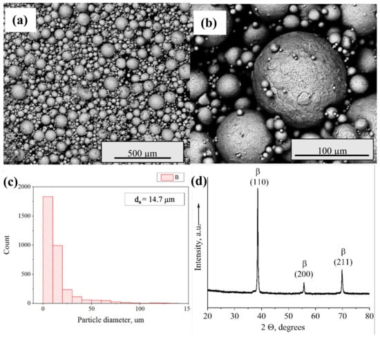
Figure 2.
SEM-images (a,b); the distribution of the powder by diameter (c), da—the average diameter of the powder with the standard deviation; XRD pattern (d) of TNZT powder obtained by spark plasma sintering and used for EBM sample manufacturing.
As expected, the XRD patterns of the pre-alloyed TNZT powder revealed only maxima attributable to the β phase (Figure 2), because the powder contains rather high concentration of β-stabilizing elements. The TNZT powder microstructure had a crystallite size of 40 nm. One should keep in mind that thermo-mechanical properties of TNZT powder are completely different from Ti-6Al-4V ones. Presintering of this powder (essential for EBM) was quite problematic. It could be due to the properties of material itself. Corresponding process parameter settings are also significantly influenced by the fact that grain size distribution of used powder is far from the one suggested for EBM machines. For better performance, more appropriate powder with more narrow grain size distribution should be used [26].
There are some studies that are mainly focused on the research of the feasibility of using a small powder size fraction and layer thickness for manufacturing components via EBM. Karlsson et al. [27,28] reported that the fine particle-size distribution of a powder and the variation in thickness between the two batches be achieved by applying the significant deviations from the standard process parameters (commercially provided by Arcam), which facilitate controlled melting and densification.
Several parameters of the EBM process have to be changed for making parts from the finer powder 25–45 µm. First, the beam focus and scanning speed during the pre-heating procedure were varied. The finer powder was more susceptible to the charges than the standard, cursor, and 45–105 µm one (charging the powder results in a widespread repulsion event mentioned as a “smoking”). The focus of the preheated beam was thus changed from 35 mA to 10 mA. The focus offset will distribute the charge over a larger area, preventing overcharging of the particles. Simultaneous alterations were introduced in the beam application strategy during preheating stage allowing more time for the powder discharging before another beam hits it. Thus, the beam speed was also increased during the preheating phase from 14.700 mm/s to 22.000 mm/s, due to the rise in current from 5 to 25 mA. To maintain the same amount of energy input and to provide a sufficient pre-heating, the number of scans was ramped to 15. To build a 25 µm layer, the thickness function parameter was reduced by 50% from standard-settings to reduce energy consumption and prevent the part swelling. The rest of the process parameters were maintained at the standard default settings for Ti6Al4V.
Samples manufactured with 25 µm build layer thickness showed lower surface roughness than the samples build with 50 μm layer. In terms of the surface roughness and overall appearance, the surfaces constructed from the finer powder had a surface with more unmelted particles attached to it, and appeared to have a higher average peak to valley ratio. The variations of thermal conductivity between the powder layers are increased, as the thickness of the building layer decreased. The thickness of the layer does not significantly affect the appearance of the surface, which is associated with the re-melting of adjacent layers. The use of different layer thicknesses and powders also made it possible to obtain the materials with the same hardness and Young’s modulus [28]. All finer powder fractions can lead to a further decrease in the thickness of the building layer and a subsequent improvement in the surface quality [27,28,29].
The manufacture of an alloy from the elementary powders in situ was discussed in [29]. The Ti particle size distribution was D10 = 26 μm, D50 = 62 μm, and D90 = 118 μm, the sizes of niobium (Nb) particles in the initial state were D10 = 12 μm, D90 = 100 μm, and D50 = 44 μm. Based on the respective melting points of Ti (1668 °C) and Nb (2477 °C), better melting and better diffusion of Nb in Ti were expected with smaller Nb particles than Ti particles. It has been demonstrated that energy has an important effect on the porosity and homogeneity of the fabricated part.
3.2. Morphology, Microstructure, and Phase Composition of TNZT Alloy
To characterize in detail the effect of the PEB treatment on microstructure, SEM analysis was conducted for the TNZT samples before Figure 3a,b and after Figure 3c,d the treatment. As the surface modification was carried out with the aim to decrease the surface roughness and to prepare the homogeneous surface morphology of TNZT alloy, the surface topography was examined by profilometry. A few pores less than 2 μm in size and some partially melted powders (~25 μm) can be observed on the untreated surfaces (Figure 3a).
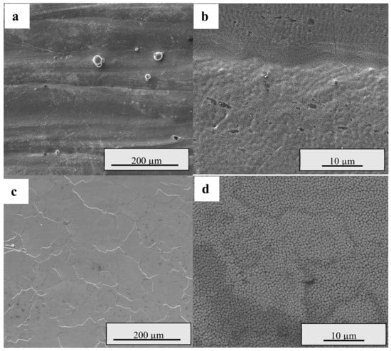
Figure 3.
SEM images of the microstructure of EBM®-manufactured TNZT alloy before (a,b) and after (c,d) PEB treatment observed at the top of the surface (last processed layer) showing cellular β (b,d) grain microstructures.
The topographical characteristics of the PEB treated surfaces have shown that after the modification the blocky grain structure is formed on the surface, which is related to the β-phase. The average grain size was measured to be 85 ± 15 μm (see Figure 3c,d). Samples after the PEB modification have an auspicious structure, rather smooth surface, and no defects, such as cracks and pores. PEB treated surface of TNZT alloy revealed the absence of significant waviness and semi-melted powder particles on the surface. In addition, it can be seen that the surface roughness decreased (Ra = 7.32 ± 0.51 μm) significantly by almost two times after the PEB treatment compared with the untreated TNZT (Ra = 12.94 ± 1.59 μm).
Thus, obtained results indicated that PEB irradiation is an effective way to modify the microstructure and surface topography of the TNZT alloy because the surface of TNZT alloy after the treatment is relatively homogeneous and shows equiaxed β-grains. Figure 3b,d show the presence of equiaxed ultra-fine domains on the top surface of the treated sample (last layer processed by EBM). The PEB treatment induces super-fast heating and melting, followed by rapid solidification of the surface layer of the material.
Sample cross-sections were investigated using the backscatter electron contrast imaging (Figure 4a,b), as well as energy-dispersive X-ray spectroscopy (EDS) (Figure 4c). Quantitative elemental analysis of four regions was conducted using an EDS detector attached to the field emission gun SEM. It was found that there was no surface composition change after the PEB treatment. Thus, the results of the EDS analysis showed that the TNZT after the PEB treatment exhibited approximately the same concentration of elements for all considered points of investigation, indicating the uniform distribution of element composition over the sample.
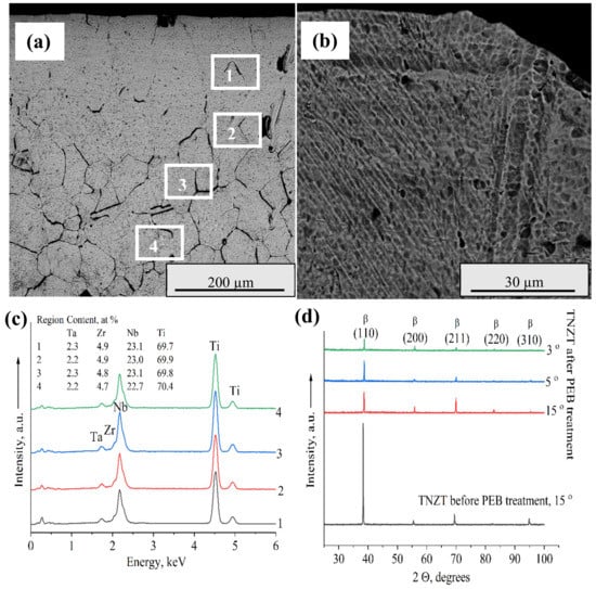
Figure 4.
(a,b) Backscatter SEM images of an as-manufactured polished and etched with Kroll’s reagent cross-section of EBM TNZT alloy after the PEB treatment. (c) EDS results for EBM-manufactured TNZT alloy after the PEB treatment at different points 1–4 on the cross-section surface. (d) Typical XRD patterns obtained at a grazing angle of 3–15° before and after the PEB treatment.
The GIXRD patterns of the EBM-manufactured TNZT alloy before and after the PEB treatment are shown in Figure 4d. It is evident that for all chosen areas surface only peaks of bcc β phase were present with the following average lattice parameters: a = 3.312 Å and 3.289 Å, for untreated and PEB treated samples, respectively. There are no peaks of hpc α phase in the diffraction patterns (Figure 4d). According to the GIXRD data, the textures of as-manufactured and irradiated TNZT samples are different (Table 2, Figure 3).
Table 2.
Influence of the PEB treatment on crystallite size (D), dislocation density (δ), and microstrain (ε) of EBM manufactured TNZT calculated from the XRD patterns obtained at a grazing angle of 15°.
PEB irradiation of the as-fabricated EBM samples of TNZT led to decrease in the intensity of (110) diffraction peak, while the (211) and (220) peaks increased intensity. It is indicated that the surface of the PEB treated samples demonstrated preferential lattice structure orientation. The texture coefficient can be used for the determination of the quantitative data concerning the preferential crystallite orientation change of the studied structures [30]:
where and are the measured and taken from the JCPDS database intensities of the diffracted from (hkl) planes for the bcc β phase of Ti, respectively. The n value is the total number of the used planes in a crystal (i.e., n = 5 in our case).
The texture coefficients of (110), (200), (211), (220), and (310) crystal planes are calculated and presented in Figure 5. The as-manufactured samples showed a preferred orientation on the (110) and (310) crystal planes. The investigation of the texture coefficient at the different grazing angle revealed the evolution of crystallite orientations at the melted zone formed at the top of the samples after the PEB treatment. In case of varying the grazing angles (3, 5, and 15 degrees) for samples after the PEB treatment, it is observed that at the top of the treated surface (at a grazing angle of 3°), growth of grains with (100) and (220) texture is favored, but with increasing grazing angle to 5°, the (211) and (310) become the preferred orientation.
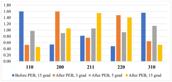
Figure 5.
Texture coefficients of the EBM manufactured TNZT alloy before and after the PEB treatment calculated for the GIXRD patterns obtained at the different grazing angle (3, 5, and 15°).
With the increase of the grazing angle to 15°, the (310) orientations decrease whereas the (211) and (220) orientations gradually decrease. However, it is found that the crystallite size [31], dislocation density [32,33], and microstrain [34] remain basically unchanged after the PEB treatment (Table 2).
From a closer observation of GIXRD patterns, it can be seen that the diffraction peaks are slightly shifted from the standard peak positions to a high angle after the PEB treatment. Thus, the initial lattice parameter of a = 3.312 Å decreases to 3.292 Å, 3.291 Å and 3.286 Å after the PEB treatment calculated at the different grazing angles of 15°, 5°, and 3°, respectively. This trend of decreasing lattice parameter with the depth of the modified surface layer can be associated with a rapid melting (even evaporating) of the studied material.
The polished cross-sections of the PEB treated TNZT alloy were etched with Kroll’s reagent to reveal the grain boundaries. In cross-sections, no clear interface line of the re-melted region after the PEB treatment was visible for all treated TNZT samples. In the PEB-treated alloy, the microstructure was markedly changed, as shown in Figure 4b,c. Although some etch pits are clearly seen on the TNZT sample treated by PEB etched with the Kroll’s reagent, a dense and homogeneous microstructure for the top layer of the samples is obtained. It should be noted that the etch pits at grain boundary triple junctions of as-manufactured TNZT alloy were also observed, which points to the rather low corrosion resistance of the material, especially at such high energy grain boundary junctions. After being etched with Kroll’s reagent, at a depth of over 100 microns the equiaxed grains of β-phase, the precipitation of α-phase along the grain boundary were observed for EBM-manufactured TNZT alloy before treatment. The residual pores represented by black contrast regions were observed along the β-phase grain boundaries. The as-manufactured Ti alloy possessed the typical blocky grain structure for EBM process [35]. The α-phase and grain boundaries are not clearly revealed near the treated surface. Therefore, the metastable β Ti–35Nb–7Zr–5Ta alloy was found to demonstrate β + α→β phase transition during the PEB irradiation. The clear evidence of the PEB-induced dissolution of α precipitates was revealed from the SEM image in Figure 3c.
The microstructural evolution and presence of α precipitate-free β phase regions of TNZT alloy are undoubtedly caused by the elevated temperatures, which are maintained by an input of energy that occurs as a result of high current PEB irradiation. It is known that the beam process parameters can influence the resulting thickness of the melted zone and heat-affected zone formed at the top of the bulk samples after the PEB treatment. The gradient surface structure treated by impulse electron beam irradiation was revealed by other authors [36]. The first top layer showed re-melted nanostructured grains [37]. The second layer becomes a heat-effected zone and may have a different structure as reported by Chen et al. [37].
The depth of the re-solidified layer depends on the PEB process parameters (the pulse energy, the number of pulses, and the melt duration) and the material characteristics (physical properties, composition, and microstructure) [38]. Jisoo Kim and Hyung Wook Park reported that the pulse energy provided more significant impact on the depth of the re-solidified layer than the number of pulses [36]. Sinyakova et al. [39] showed that the increase in electron beam energy density from 12 J cm−2 to 24 J cm−2 leads to the growth of irradiated layer thickness from 25 μm to 80 μm, respectively. Thus, the phase composition and structural parameters of the as-manufactured TNZT alloy could be changed at the upper surface layer.
As mentioned before electron beam melting of TNZT powder retains a single β phase with a = 3.2931 Å in the as-manufactured TNZT alloy. EBM-manufactured TNZT alloy also shows a preferred [001]β crystallographic orientation along the growth direction during the fabrication. It is well known that the β phase of Ti provides lower elastic modulus than the α phase, due to this the β-Ti alloys may fill most of the imposed demands for an ideal biocompatible alloy for bone substitution [40].
The microstructure of the top layer of the EBM-manufactured TNZT alloy before and after the PEB treatment was further studied using TEM to capture microstructural features that could not be resolved by SEM and XRD. Figure 6 shows the bright-field images and corresponding selected area electron diffraction (SAED) pattern of the EBM-manufactured TNZT alloy before the PEB treatment. As seen from Figure 6, the TNZT consists mainly of β-Ti. A large number of dislocations are observed in the grain interiors. According to the indexed SAED pattern in Figure 6c, the white circle marked region in the bright-field TEM image (Figure 6b) comprised β and NbTi4 phase, which was also confirmed by the dark-field TEM image in Figure 6d. The nanocrystalline precipitates of the intermetallic compound NbTi4 are observed. This compound shows an orthorhombic crystal structure in the space group Cmcm.
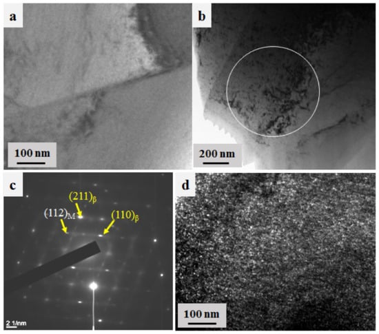
Figure 6.
TEM analysis of the EBM-manufactured TNZT alloy after the PEB treatment. (a,b) TEM bright-field images; (c) corresponding SEAD pattern recorded from the white circle marked region in (b); (d) TEM dark-field image obtained using the (112)M spot indicated in (c).
Although α phase was not found by SEM and XRD, α precipitates were detected by TEM (Figure 7). The spotty diffraction peaks in the SAED pattern indicated the presence of hcp α and NbTi4 phases. Dark-field TEM images recorded from (100)α and (002)α reflections show that α phase is not distributed homogeneously inside the β matrix of TNZT alloy. These fine scale α precipitates are spherical, with the size of approximately 10 nm, as seen in the dark-field TEM image.
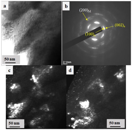
Figure 7.
TEM analysis of the EBM-manufactured TNZT alloy after the PEB treatment by. (a) TEM bright-field image; (c) corresponding SEAD pattern recorded from the region in (a); (c,d) TEM dark-field images obtained using the (100)α and (002)α spots, respectively, indicated in (b).
Previous reports in the literature suggested that α- phase preferentially nucleates at the defects in β-solution, such as dislocations, intermetallic compounds, and grain boundaries [41,42]. The presence of two phases of the β with bcc structure and the α″-martensite with orthorhombic structure in the Ti–24Nb–4Zr–7.9Sn (wt%) alloy fabricated by EBM from the pre-alloyed, rapidly-solidified precursor powder was reported by Hernandez J. et al. [35].
The bright-field TEM image and corresponding SAED pattern of TNZT alloy treated by PEB showed that the top region of the as-built sample was mainly composed of randomly distributed sub-microscale β grains with the average size of 200 ± 80 nm. As observed in Figure 8, the microstructure is featured by grains with rather low dislocation density and well-defined grain boundaries. Relatively straight morphology of the dislocations was basically revealed.
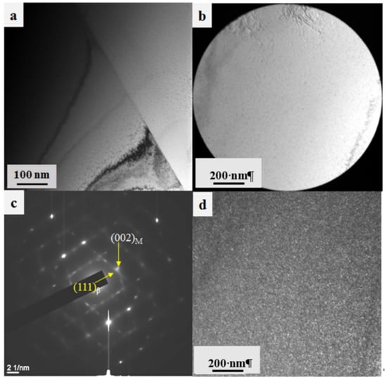
Figure 8.
Ti–35Nb–7Zr–5Ta alloy obtained by EBM. (a,b) bright-field TEM images and (c) corresponding SAED pattern recorded from the region in (a) showing the absence of α phase, (d) Dark field TEM image taken from the diffraction (002)M spot indicated in (c).
The same results were observed by Gao Y.K. [21]. It was reported that, when the pulsed energy density is 20 J·cm−2, the modified surface layer of the pure Ti will contain fewer dislocations and a larger number of subgrains. The diffraction pattern of as-built TNZT showed reflections corresponding to the NbTi4 phase along with those of the β phase. The very fine-scale NbTi4 precipitates are evident in the dark-field TEM image. However, the microstructure of as-manufactured TNZT alloy after the PEB irradiation revealed no evidence of α phase precipitation.
Therefore, a careful comparison of the microstructure of TNZT before and after the PEB treatment revealed the presence of martensite NbTi4 phase with the orthorhombic system. NbTi4 is a non-equilibrium compound that will not be able to determine using the phase diagram of the equilibrium Ti–Nb system [43]. The orthorhombic NbTi4 phase (M) was found by Li, Y. et al. for Ti-10Nb-5Sn alloy heated and cooled repeatedly in a heated system located in a TEM chamber [44]. The mechanism of the transformation between austenite β and martensite phase was observed in situ using a high-resolution TEM. The authors reported that the crystal plane ()β transforms into (001)M during the transformation from β to M phases. The martensite transformation mechanism involves the (100)β and (011)β transforming to (100)M and (010)M through the tiny migration of atoms. In addition, intermetallic precipitates of NbTi4 were detected for Ti-Nb-based alloys obtained by high-energy ball milling by Salvo C. et al. [45] and in the laser fusion zone obtained via Nd:YAG laser welding technique by Bahador A. et al. [46].
3.3. Corrosion Test Results
The corrosion resistance of TNZT alloy treated by PEB was investigated by linear polarization resistance technique in order to acquire the polarization resistance (Rp), Tafel plots (for determining the electrochemical parameters), and for the evaluation of breakdown potential in Hanks’ solution by EIS technique. The experimental results were compared for PEB-treated and untreated as-manufactured TNZT alloy. Results of open circuit potential (OCP) measurements for TNZT alloy in Hank’s solution are presented in Figure 9. An increase in the potential at early times was identified for both untreated and the PEB-treated TNZT alloy due to the growth of a passive layer over the surface.
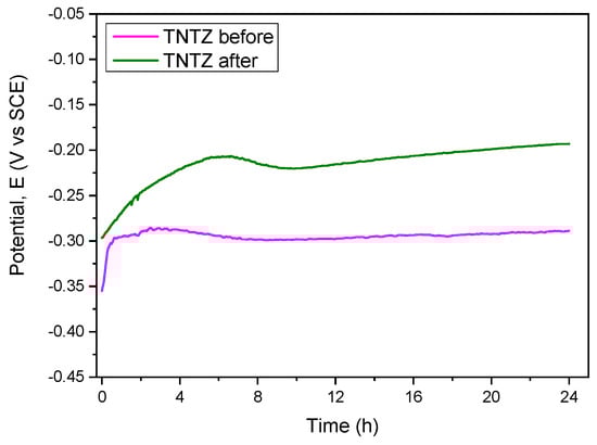
Figure 9.
Corrosion potential–time behavior of EBM-fabricated TNTZ alloy before and after the PEB treatment in Hank’s solution.
For the TNZT alloy after the PEB treatment, almost immediately after the immersion, the open circuit potential reached a value of −0.30 V relatively stable until the end of the test. This result indicates that the surface of as-built TNZT is stable from the beginning and the formed oxide is stable, which may assure good protection to corrosion. The OCP of the initial TNZT sample reaches −300 mV compared to the saturated calomel electrode (SCE) after approximately 83,000 s immersion initially. The TNZT sample takes ~3400 s to reach approximately from −350 mV to −300 mV compared to the SCE, an almost stable potential. This behavior suggests that the protective passive layer is formed rapidly on the alloy surface. The PEB-treated TNZT alloy demonstrated a more positive OCP as compared to that of the untreated sample. After the PEB irradiation, the potential increased up to −220 mV and stabilized after ~8 h, suggesting better preservation and higher stability of the protective passive layer and a consequent improvement in the material corrosion resistance. A more gradual change towards more positive potentials was revealed for the treated TNZT alloy, which indicates an oxide layer gradually formed on the alloy surface. Thus, Eoc = −288.84 mV for TNZT alloy before the PEB treatment, which is lower than Eoc = −193.07 for TNZT alloy after the PEB modification. Obtained results suggested that the TNZT alloy after the PEB irradiation has better corrosion resistance (Table 3).
Table 3.
Main electrochemical parameters extracted from Tafel plots.
Potentiodynamic anodic polarization curves for the EBM-fabricated TNZT alloy before and after the PEB treatment in Hank’s solution are presented in Figure 10. No pitting- defined features are observed in both curves, which means that both the PEB treated and as-manufactured TNZT alloy surfaces show excellent resistance to localized corrosion. The main corrosion parameters acquired from Hank’s solution experiments are summarized in Table 3. The lowest corrosion potential of −193 mV was determined from the Tafel-type fit on the EBM- manufactured TNZT alloy before the treatment (Table 3). EBM fabricated TNZT alloy after the PEB treatment showed a higher corrosion current density value compared to that of an as-manufactured one.
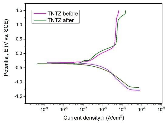
Figure 10.
Potentiodynamic curves of the irradiated and initial TNZT alloy treated in Hank’s solution.
From Figure 10, it is clear that the current density is seen to decrease with increasing potentialin the cathodic branch, and when the potential (Ecorr) reaches a certain value while keeping the upward trend (in anodic branch), the current density starts growing.
Also, the icorr value is not so different for the as manufactured and PEB treated TNZT. Corresponding icorr value for treated TNTZ is higher, but not significantly. The same evolution can be seen in the case of polarization resistance Rp. It is well accepted that a surface is resistant to corrosion when the icorr is low and Rp high. From our experiments, it can be stated that the surface corrosion resistance after the treatment is increased but not significantly improved. It can be also observed that the breakdown potentials have quite similar values. Taking into account the potentiodynamic curves, for the as-built TNZT sample, the passivation domain is ranged from 263 to 1185 mV, while for the PEB treated TNZT from 312 to 1161 mV. Both investigated surfaces exhibited a passivation potential around of 900 mV.
It is generally accepted that the corrosion behavior of Ti alloys is strongly dependent on several factors such as composition and microstructure. Moreover, it has been widely realized that the corrosion performance of Ti alloys is strongly influenced by the surface state (e.g., roughness and purity), the grain size (grain boundary), and crystal defects (dislocation and twin). In this study, significant differences were found among the microstructure of the EBM-manufactured TNZT alloy before and after the PEB treatment. The typical reported values of corrosion current density (icorr) for TNZT alloys are approximately 300−500 mV, which were obtained under similar conditions of testing in Hank’s solution.
Nyquist plots for as-manufactured and PEB-treated TNTZ alloy are presented in Figure 11. It can be noted that the magnitude of the impedance increased after the treatment of alloy. However, both spectra have an incomplete semicircle, which can be associated with a highly capacitive behavior at the lower potentials. It means that the corresponding inductance in the equivalent circuit can be omitted.
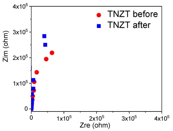
Figure 11.
Nyquist plot of TNTZ alloy in Hank’s solution.
The Bode plot of TNTZ alloys tested in Hank’s solution at its respective Ecorr for 1 h can be observed in Figure 12 together with the equivalent circuit representation. For both treated and untreated TNZT the phase angle decreased towards zero in the higher-frequency region corresponding to the presence of electrolytic reactions. In Bode plots of the PEB-treated samples, the phase angle is generally higher, indicating that the treatment effectively leads to an increase in anti-corrosion behavior.
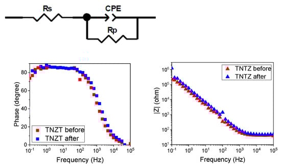
Figure 12.
Bode plot of TNTZ alloys in Hank’s solution at Ecorr.
For TNTZ alloy the main impedance parameters are listed in Table 4. It was found that the TNTZ alloy showed increased resistance and its capacitance decreased after the treatment with increasing impressed potential. It is well known that sample capacitance is closely related to the geometry of the electrode surface. Also, when the surface double-layer is affected by the charge transfer it is leading to a significant deviation of effective capacitance behavior from the ideal electric double-layer case. After the treatment, effective capacitance values have increased about twice, indicating that the electrolyte molecules are adsorbed on the surface of treated TNTZ alloy, which is also sustained by much higher values of Rs and Rp as compared to untreated TNTZ alloy. High Rp values and indicate that equivalent capacitance has a low leakage current and is close to ideal electrical-circuit representation. A similar conclusion comes from the fact that fitting parameter α is close to 1 as it should be for ideal capacitance (for ideal resistance it should be 0).
Table 4.
Main electrical parameters extracted from EIS measurement: Rs—solution resistance between the material and reference electrode; C—material capacitance; α—parameter associated to the CPE used for fitting of the data (CPE was used in the current fitting due to the non-ideal character of the material); Rp—resistance at the electrolyte-material interface.
Resistance at the electrolyte-material interface was found to be higher for the TNTZ after treatment, signifying that this surface is more resistant to corrosion. To conclude the EIS tests, the TNTZ alloy after the treatment is more resistant to Hank solution attack due to the formation of a passive film over the surface.
It is well established that the improved surface properties of metals and alloys after the PEB treatment are determined by the final microstructure and composition homogenization of the surface layer. Recent research into corrosion of Ti-6Al-7Nb alloy treated of large PEB has shown the improved corrosion resistance after the treatment due to the formation of a re-solidified passivation layer [36]. Zhang et al. investigated the surface treatment of stainless steels and revealed the improved corrosion resistance after high current PEB modification due to the composition homogenizations and selective surface purification effect [47].
3.4. Mechanical Properties
To study the effect of the PEB treatment on the mechanical properties, the hardness (H) and Young’s modulus (E) was measured for the cross-section of the treated TNZT alloy samples after the etching with Kroll’s reagent for 10 min using nanoindentation. The variation of H and E along the depth of the treated TNZT alloy is presented in Figure 13. It can be seen that the highest H and E values of the PEB treated alloy was found near the alloy surface. Although the depth of the hardened surface layer does not exceed 100 μm.
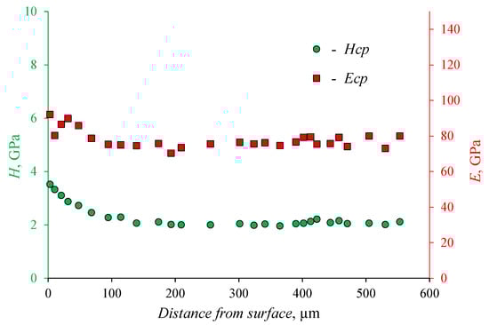
Figure 13.
The hardness and Young’s modulus distribution of the cross-section of the PEB treated TNZT samples manufactured by EBM along the depth (sample was etched with Kroll’s reagent for 10 min).
Thus, the hardness near the surface after the PEB treatment was 3.33 GPa, which corresponds to 32% enhancement from as-manufactured samples. Deeper into the TNZT material, the hardening effect becomes less evident, and finally disappears at the penetration depth of ~100 μm, which is consistent with the depth of the PEB-treated layer in Figure 14. The E near the surface was 92 GPa, corresponding to only 18.5% enhancement. The H and E values obtained for the top surface layer consisting of nanograins revealed higher values than these of the bulk matrix. The PEB treatment of TNZT alloy provided a continuous and gradual decrease in H and E profile gradient. It was observed that the microstructure and properties of the PEB treated counterpart fabricated by additive manufacturing are anisotropic.
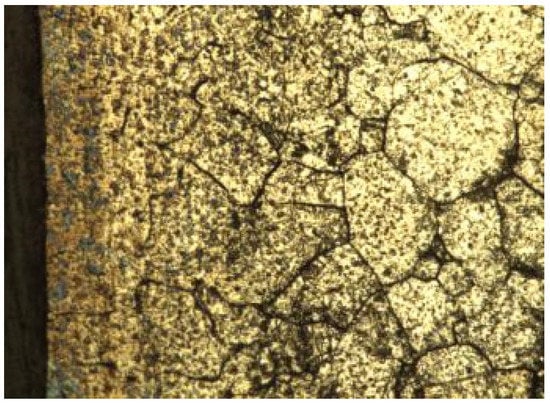
Figure 14.
An optical image of the PEB treated TZNT surface after the etching for 10 min in the indentation region. The size of the area shown in the image is 540 × 390 microns.
Based on the cross-section image of the TNZT sample and mechanical properties analysis (Figure 13 and Figure 14), a better understanding of the irradiation effect on the changes in the microstructure along with the depth, and the correlation of these changes with the corresponding variation of the mechanical properties were obtained. Three different regions are detected: rather homogenous re-melted layer, heat-affected zone, and the region corresponding to the untreated bulk material of the sample. The thickness of the melted surface layer and the heat-affected zone are about 90–100 and 140 μm, respectively. Figure 14 illustrates how the grain size gradually increases with the depth from the treated surface of the TNZT alloy. Thus, the PEB treatment leads to the recomposition of coarse-grained structure into porosity-free and homogeneous in chemical composition surface.
However, only two visible areas of the H vs. S and E vs. S can be detected in the plots presented in Figure 13: (i) the one with the gradually decreasing of the H and, E values, which well agrees with the thickness of the re-melted surface layer (Figure 14); and (ii) the one with the rather stable H and E values typical for TNZT alloy [48,49]. Thus, it can be concluded that the PEB irradiation changes the H and E values only for the surface areas of the TNZT alloy manufactured by EBM. The small material hardening at the area of the re-melted surface layer can be interpreted through the nanograins formation after the PEB treatment. It was mentioned before that the treated surface of TNZT alloy was characterized by uniformly distributed nanometer-scale grains with a mean grain size ~85 nm (Figure 3).
Moreover, the PEB treatment allows fabricating porosity-free and homogeneous in chemical composition surface that only slightly affects the mechanical properties of the components. It was reported that the main effect of the PEB irradiation on the mechanical properties of Ti or Ti6Al4V alloy was surface hardening [21,50]. The similar values of the E were determined by nanoindentation for the TNZT alloy prepared in a vacuum arc melting followed by the homogenization, re-melting, and heat-treatment. The authors of study the [51] reported two reasons for the reduction of E in the studied materials. The first reason is the presence of a significant number of crystalline defects such as grain boundaries, and the second one is the complete elimination of the ω phase from the β phase matrix. Therefore, an increase in the proportion of grain boundary areas could decrease the E of the material.
It is known, that Ti alloys may reveal the presence of the equilibrium lattice structures (hcp α- and bcc β-phases), or metastable ones (hcp α′ martensite, orthorhombic α″ martensite, and the hexagonal ω-phase) in dependence of the alloy composition and thermomechanical process, which can occur during the sample preparation and/or treatment. Sinyakova, E. A., et al. [39] reported that PEB treatment exhibited the formation of α′ and α″ phases in the melted surface layer of Ti-6Al-4V alloy. Meanwhile, Sankara et al. [52] showed that the PEB irradiation has led to a transformation of the α + β dual phase to a single α′-martensite phase on the surface of the Ti-6Al-4V alloy. It was demonstrated by Yao et al. [53] that the microstructure of Ti–Zr (67.0 Ti, 32.3 Zr, and 0.7 Cr) revealed α plate decomposition through α → β + ω + α route during the laser surface re-melting treatment. Moreover, the formation of fine ω and α phases were observed, which were uniformly distributed within the β matrix. The study by Zhang X.D. et al. [54] demonstrated that although the starting microstructure of the TA15 alloy (6.5 wt% Al, 2 wt% Zr, 1 wt% Mo, 1 wt% V and Ti balance) composed of α equiaxed grains with the few β phase particles and the β phase formed first from the melt under the rapid solidification process, both the re-melted layer and solid-state transformation layer of the PEB treated samples revealed the presence of only α’ martensite after the cooling, and β phase has disappeared. Nevertheless, below the re-melted layer, the following phase transformation path occurred: β + α → β + β(α--rich) during heating followed by the β + β(α--rich) → β + α′ transformation during cooling. Marczewski et al. [55] demonstrated that the increase in content of the β Ti phase in the near-β type Ti-Zr-Nb alloy (36 ≤ Ti ≤ 70 at. %) could be performed by the increasing processing time of the mechanical alloying. The effect of the processing parameters on the phase compositions and microstructural features of EBM treated Ti–36Nb–2Ta–3Zr–0.35O alloys was discussed by Chen et al. [37]. It was observed that the scanning speed had increased the microstructural changes from the highly dispersed acicular ɑ″ phase to the formation of cellular grains and α′ phase. However, although the main effect of the PEB modification on the mechanical properties of α- Ti or and α+β phase Ti alloy where α- phase dominates was the hardening. In the present study, we observed that the PEB treatment did not significantly change the H and E values measured for the β phase TNZT alloy produced by EBM for the chosen PEB treatment parameters.
4. Conclusions
The finishing process using the PEB irradiation was used for treating TNZT alloys produced by EBM. The present study examined that the microstructure, microhardness, and corrosion behavior properties of the PEB-treated EBM-fabricated TNZT alloy are comparable to those of the as-built material. The corrosion resistance of the alloy was evaluated via an electrochemical method. The changes were found by SEM in the surface properties of TNZT alloy after the PEB treatment. The unmelted and partially melted powder particles as well as pores were eliminated on the surface of the EBM-manufactured TNZT alloy after the PEB-treatment. The surface of TNZT alloy after the PEB treatment is relatively homogeneous and shows equiaxed β-grains. TEM investigations revealed that TNZT alloy manufactured by EBM exhibited the β phase matrix with the fine NbTi4 precipitates. Therefore, the metastable β Ti–35Nb–7Zr–5Ta alloy was found, which indicate the existence of β+α→β phase transition during the PEB irradiation. The evidence of the PEB-induced dissolution of α precipitates was detected from the TEM and SEM studies. The PEB treatment resulted in the increase of the corrosion current densities of the EBM-manufactured TNZT alloy. The PEB treatment of the alloy surface reported in this study can effectively improve the corrosion resistance of EMB-manufactured TNZT alloy. The differences in corrosion resistance between the untreated and treated by PEB samples, indicating the existence of variations in the microstructures and composition of the top surface re-melted layer. The Young’s modulus and hardness near the TNZT surface after the PEB treatment were measured to be 18.5 and 38% higher than the values obtained for the as-manufactured coarse-grained alloy. Therefore, the PEB treatment is a viable approach that allows one to prepare porosity-free and smooth surface for property measurements and application with different microstructure, but the same mechanical features.
Author Contributions
Conceptualization, M.S., A.K., R.S.; methodology, A.V. (Alina Vladescu), C.M.C., A.T. (Alexander Tyurin), A.K., N.K.; measurements Y.I., A.T. (Anton Teresov), A.V. (Alina Vladescu), C.M.C.; investigation, M.S., I.G., N.G., A.V. (Anastasia Volkova), D.K.; writing—original draft preparation, M.S., I.G.; writing—review and editing A.K., A.V., C.M.C., A.T. (Alexander Tyurin), N.K. and R.S.; supervision, M.S.; funding acquisition, I.G. and M.S. All authors have read and agreed to the published version of the manuscript.
Funding
Authors acknowledge RSF grant no. 20-73-10223 for the financial support of the sample fabrication part, and Ministry of Science and Higher Education of the Russian Federation (State Project “Science” N◦WSWW-2020-0011) for the financial support of the sample characterization part.
Data Availability Statement
The data presented in this study are available on request from the corresponding author. The data are not publicly available as they also form part of an ongoing study.
Acknowledgments
Authors thank O.I. Mishukova (National Research Tomsk Polytechnic University, Russia) and E. Ivanov (Tosoh SMD Inc., USA) for the help with the sample preparation.
Conflicts of Interest
The authors declare no conflict of interest.
References
- Niinomi, M. Recent research and development in titanium alloys for biomedical applications and healthcare goods. Sci. Technol. Adv. Mater. 2003, 4, 445–454. [Google Scholar] [CrossRef]
- Long, M.; Rack, J. Titanium alloys in total joint replacement—A materials science perspective. Biomaterials 1998, 19, 1621–1639. [Google Scholar] [CrossRef]
- Kurtz, S.; Ong, K.; Lau, E.; Mowat, F.; Halpern, M. Projections of primary and revision hip and knee arthroplasty in the United States from 2005 to 2030. J. Bone Jt. Surg. 2007, 89, 780–785. [Google Scholar] [CrossRef]
- Brehme, H.J. Titanium and titanium alloys, biomaterials of preference. Mémoires études Sci. Rev. Métallurgie 1989, 86, 625–637. [Google Scholar]
- De Gélas, B.; Molinier, R.; Séraphin, L.; Armand, M.; Tricot, R. A Titanium Alloy with Improved Mechanical Resistance Ti-6A1-6V-2Sn-6Zr. In Titanium and Titanium Alloys; Springer: Boston, MA, USA, 1982; pp. 2121–2130. [Google Scholar]
- Sowa, M.; Parafiniuk, M.; Mouzelo, C.M.S.; Kazek-KęsikaIvan, A.; Zhidkov, I.S.; Kukharenko, A.I.; Cholakh, O.; Kurmaev, E.Z.; Simka, E. DC plasma electrolytic oxidation treatment of gum metal for dental implants. Electrochim. Acta 2019, 302, 10–20. [Google Scholar] [CrossRef]
- Lee, Y.-S.; Niinomi, M.; Nakai, M.; Narita, K.; Cho, K. Predominant factor determining wear properties of β-type and (α+β)-type titanium alloys in metal-to-metal contact for biomedical applications J. Mech. Behav. Biomed. Mater. 2015, 41, 208–220. [Google Scholar] [CrossRef]
- Ahmadi, S.M.; Hedayati, R.; Ashok Kumar Jain, R.K.; Li, Y.; Leeflang, S.; Zadpoor, A.A. Effects of laser processing parameters on the mechanical properties, topology, and microstructure of additively manufactured porous metallic biomaterials: A vector-based approach. Mater. Des. 2017, 134, 234–243. [Google Scholar] [CrossRef]
- Banerjee, R.; Nag, S.; Samuel, S.; Fraser, H.L. Laser-deposited Ti-Nb-Zr-Ta orthopedic alloys. J. Biomed. Mater. Res. Part A 2006, 78, 298–305. [Google Scholar] [CrossRef] [PubMed]
- Murr, L.E.; Gaytan, S.M.; Ceylan, A.; Martinez, E.; Martinez, J.L.; Hernandez, D.H.; Machado, B.I.; Ramirez, D.A.; Medina, F.; Collins, S.; et al. Characterization of titanium aluminide alloy components fabricated by additive manufacturing using electron beam melting. Acta Mater. 2010, 58, 1887–1894. [Google Scholar] [CrossRef]
- Chan, K.S.; Koike, M.; Mason, R.L.; Okabe, T. Fatigue life of titanium alloys fabricated by additive layer manufacturing techniques for dental implants. Metall. Mater. Trans. A 2013, 44, 1010–1022. [Google Scholar] [CrossRef]
- Liu, X.; Chu, P.K.; Ding, C. Surface modification of titanium, titanium alloys, and related materials for biomedical applications. Mater. Sci. Eng. 2004, 47, 49–121. [Google Scholar] [CrossRef]
- Niinomi, M.; Liu, Y.; Nakai, M.; Liu, H.; Li, H. Biomedical titanium alloys with Young’s moduli close to that of cortical bone. Regen. Biomater. 2016, 3, 173–185. [Google Scholar] [CrossRef] [PubMed]
- Nakai, M.; Niinomi, M.; Akahori, T.; Ohtsu, N.; Nishimura, H.; Toda, H. Surface hardening of biomedical Ti-29Nb-13Ta-4.6 Zr and Ti-6Al-4V ELI by gas nitriding. Mater. Sci. Eng. A 2008, 486, 193–201. [Google Scholar] [CrossRef]
- Mridha, S.; Baker, T. Effects of nitrogen gas flow rates on the microstructure and properties of laser-nitrided IMI318 titanium alloy (Ti-4V-6Al). J. Mater. Process. Technol. 1998, 77, 115–121. [Google Scholar] [CrossRef]
- Rastkar, A.; Bell, T. Characterization and tribological performance of oxide layers on a gamma based titanium aluminide. Wear 2005, 258, 1616–1624. [Google Scholar] [CrossRef]
- Wang, Y.; Qian, Z.; Li, X.; Tandon, K. Sliding wear properties of TiAl alloys with/without TiN coatings. Surf. Coat. Technol. 1997, 91, 37–42. [Google Scholar] [CrossRef]
- Oliveira, N.T.; Guastaldi, F.P.; Perrotti, V.; Hochuli-Vieira, E.; Guastaldi, A.C.; Piattelli, A.; Lezzi, G. Biomedical Ti-Mo alloys with surface machined and modified by laser beam: Biomechanical, histological, and histometric analysis in rabbits. Clin. Implant Dent. Relat. Res. 2013, 15, 427–437. [Google Scholar] [CrossRef]
- Zhang, X.; Hao, S.; Li, X.; Dong, C.; Grosdidier, T. Surface modification of pure titanium by pulsed electron beam. Appl. Surf. Sci. 2011, 257, 5899–5902. [Google Scholar] [CrossRef]
- Proskurovsky, D.; Rotshtein, V.; Ozur, G.; Ivanov, Y.F.; Markov, A. Physical foundations for surface treatment of materials with low energy, high current electron beams. Surf. Coat. Technol. 2000, 125, 49–56. [Google Scholar] [CrossRef]
- Gao, Y. Surface modification of TA2 pure titanium by low energy high current pulsed electron beam treatments. Appl. Surf. Sci. 2011, 257, 7455–7460. [Google Scholar] [CrossRef]
- Koval, N.N.; Ivanov, Y.F. Nanostructuring of surfaces of metalloceramic and ceramic materials by electron beams. Russ. Phys. J. 2008, 51, 505–516. [Google Scholar] [CrossRef]
- Uglov, V.V.; Kuleshov, A.K.; Soldatenko, E.A.; Koval, N.N.; Ivanov, Y.F.; Teresov, A.D. Structure, phase composition and mechanical properties of hard alloy treated by intense pulsed electron beams. Surf. Coat. Technol. 2012, 206, 2972–2976. [Google Scholar] [CrossRef]
- Rechtin, J.; Torresani, E.; Ivanov, E.; Olevsky, E. Fabrication of titanium-niobium-zirconium-tantalium alloy (TNZT) bioimplant components with controllable porosity by spark plasma sintering. Materials 2018, 11, 181. [Google Scholar] [CrossRef]
- Surmeneva, M.A.; Koptyug, A.; Khrapov, D.; Ivanov, Y.F.; Mishurov, T.; Evsevleev, S.; Prymak, O.; Loza, K.; Epple, M.; Bruno, G.; et al. In situ synthesis of a binary Ti-10at% Nb alloy by electron beam melting using a mixture of elemental niobium and titanium powders. J. Mater. Process. Technol. 2020, 282, 116646. [Google Scholar] [CrossRef]
- Chen, S.Y.; Huang, J.C.; Pan, C.T.; Lin, C.H.; Yang, T.L.; Huang, Y.S.; Ou, C.H.; Chen, L.Y.; Lin, D.Y.; Lin, H.K.; et al. Microstructure and mechanical properties of open-cell porous Ti-6Al-4V fabricated by selective laser melting. J. Alloys Compd. 2017, 713, 248–254. [Google Scholar] [CrossRef]
- Algardh, J.K.; Horn, T.; West, H.; Aman, R.; Snis, A.; Engqvist, H.; Lausmaa, J.; Harrysson, O. Thickness dependency of mechanical properties for thin-walled titanium parts manufactured by Electron Beam Melting (EBM)®. Addit. Manuf. 2016, 12, 45–50. [Google Scholar] [CrossRef]
- Karlsson, J.; Snis, A.; Engqvist, H.; Lausmaa, J. Characterization and comparison of materials produced by Electron Beam Melting (EBM) of two different Ti-6Al-4V powder fractions. J. Mater. Process. Technol. 2013, 213, 2109–2118. [Google Scholar] [CrossRef]
- Fischer, M.; Joguet, D.; Robin, G.; Peltier, L.; Laheurte, P. In situ elaboration of a binary Ti-26Nb alloy by selective laser melting of elemental titanium and niobium mixed powders. Mater. Sci. Eng. C 2016, 62, 852–859. [Google Scholar] [CrossRef] [PubMed]
- Barret, C.S.; Massalski, T.B. Structure of Metals; Pergamon Press: Oxford, UK, 1980. [Google Scholar]
- Varin, R.A.; Bystrzycki, J.; Calka, A. Effect of annealing on the microstructure, ordering and microhardness of ball milled cubic (L12) titanium trialuminide intermetallic powder. Intermetallics 1999, 7, 785–796. [Google Scholar] [CrossRef]
- Dongol, M.; El-Denglawey, A.; Elhady, A.F.; Abuelwafa, A.A. Structural properties of nano 5, 10, 15, 20-Tetraphenyl-21H, 23H-porphine nickel (II) thin films. Curr. Appl. Phys. 2012, 12, 1334–1339. [Google Scholar] [CrossRef]
- Laugier, J.; Bochu, B. LMGP-Suite of Programs for the Interpretation of Xray Experiments; BP46.38042; ENSP/Laboratories des Materiaux et du Genie Physique: Saint Martin d’Heres, France, 2000. [Google Scholar]
- Stokes, A.R.; Wilson, A.J.C. The diffraction of X rays by distorted crystal aggregates-I. Proc. Phys. Soc. 1944, 56, 174–181. [Google Scholar] [CrossRef]
- Hernandez, J.; Li, S.J.; Martinez, E.; Murr, L.E.; Pan, X.M.; Amato, K.N.; Cheng, X.Y.; Yang, F.; Terrazas, C.A.; Gaytan, S.M.; et al. Microstructures and hardness properties for β-phase Ti-24Nb-4Zr-7.9 Sn alloy fabricated by electron beam melting. J. Mater. Sci. Technol. 2013, 29, 1011–1017. [Google Scholar]
- Kim, J.; Park, H.W. Influence of a large pulsed electron beam (LPEB) on the corrosion resistance of Ti-6Al-7Nb alloys. Corros. Sci. 2015, 90, 153–160. [Google Scholar] [CrossRef]
- Chen, Z.; Liu, Y.; Wu, H.; Zhang, W.; Guo, W.; Tang, H.; Liu, N. Microstructures and wear properties of surface treated Ti-36Nb-2Ta-3Zr-0.35 O alloy by electron beam melting (EBM). Appl. Surf. Sci. 2015, 357, 2347–2354. [Google Scholar] [CrossRef]
- Zhang, T.C.; Zhang, K.M.; Zou, J.X.; Yan, P.; Yang, H.Y.; Song, L.X.; Zhang, X. Surface microstructure and property modifications in a Mg-8Gd-3Y-0.5 Zr magnesium alloy treated by high current pulsed electron beam. J. Alloys Compd. 2019, 788, 231–239. [Google Scholar] [CrossRef]
- Sinyakova, E.A.; Panin, A.V.; Perevalova, O.B.; Shugurov, A.R.; Kalashnikov, M.P.; Teresov, A.D. The effect of phase transformations on the recovery of pulsed electron beam irradiated Ti-6Al-4V titanium alloy during scratching. J. Alloys Compd. 2019, 795, 275–283. [Google Scholar] [CrossRef]
- Taddei, E.B.; Henriques, V.A.R.; Da Silva, R.M.; Cairo, C.A.A. Age-hardening of Ti-35Nb-7Zr-5Ta alloy for orthopaedic implants. Mater. Res. 2007, 10, 289–292. [Google Scholar] [CrossRef][Green Version]
- Guo, S.; Meng, Q.; Zhao, X.; Wei, Q.; Xu, H. Design and fabrication of a metastable β-type titanium alloy with ultralow elastic modulus and high strength. Sci. Rep. 2015, 5, 14688. [Google Scholar] [CrossRef] [PubMed]
- Nag, S.; Banerjee, R.; Srinivasan, R.; Hwang, J.Y.; Harper, M.; Fraser, H.L. Omega-Assisted nucleation and growth of α precipitates in the Ti–5Al–5Mo–5V–3Cr–0.5Fe β titanium alloy. Acta Mater. 2009, 57, 2136–2147. [Google Scholar] [CrossRef]
- Baker, H. Introduction to Alloy Phase Diagrams; ASM International: Materials Park, OH, USA, 1992; p. 1.1. [Google Scholar]
- Li, Y.; Qi, J.; Fan, R.R.; Zhai, C.X.; Xu, C.H. In Situ TEM Observation of Phase Transformation for Bio-Medical Shape Memory TiNbSn Alloy. Adv. Mater. Res. 2010, 152, 1755–1758. [Google Scholar] [CrossRef]
- Salvo, C.; Aguilar, C.; Cardoso-Gil, R.; Medina, A.; Bejar, L.; Mangalaraja, R. Study on the microstructural evolution of Ti-Nb based alloy obtained by high-energy ball milling. J. Alloys Compd. 2017, 720, 254–263. [Google Scholar] [CrossRef]
- Bahador, A.; Saud, S.; Hamzah, E.; Abubakar, T.; Yusof, F.; Ibrahim, M.K. Nd:YAG laser welding of Ti-27 at.% Nb shape memory alloys. Weld. World 2016, 60, 1133–1139. [Google Scholar] [CrossRef]
- Zhang, K.M.; Zou, J.X.; Grosdidier, T.; Dong, C.; Yang, D. Improved pitting corrosion resistance of AISI 316L stainless steel treated by high current pulsed electron beam. Surf. Coating. Technol. 2006, 201, 1393–1400. [Google Scholar] [CrossRef]
- Banerjee, R.; Nag, S.; Stechschulte, J.; Fraser, H.L. Strengthening mechanisms in Ti-Nb-Zr-Ta and Ti-Mo-Zr-Fe orthopaedic alloys. Biomaterials 2004, 25, 3413–3419. [Google Scholar] [CrossRef]
- You, L.; Song, X. A study of low Young′s modulus Ti–Nb–Zr alloys using d electrons alloy theory. Scr. Mater. 2012, 67, 57–60. [Google Scholar] [CrossRef]
- Surmeneva, M.; Surmenev, R.; Tyurin, A.; Mukhametkaliyev, T.; Teresov, A.; Koval, N.; Pirozhkova, T.; Shuvarin, I.; Oehr, C. Comparative study of the radio-frequency magnetron sputter deposited CaP films fabricated onto acid-etched or pulsed electron beam-treated titanium. Thin Solid Films 2014, 571, 218–224. [Google Scholar] [CrossRef]
- Xie, Y.X.K.; Wang, Y.; Zhao, Y.; Chang, L.; Wang, G.; Chen, Z.; Cao, Y.; Liao, X.; Lavernia, E.J.; Valiev, R.Z.; et al. Nanocrystalline β-Ti alloy with high hardness, low Young’s modulus and excellent in vitro biocompatibility for biomedical applications. Mater. Sci. Eng. C 2013, 33, 3530–3536. [Google Scholar] [CrossRef] [PubMed]
- Narayanan, T.S.; Kim, J.; Park, H.W. High performance corrosion and wear resistant Ti-6Al-4V alloy by the hybrid treatment method. Appl. Surf. Sci. 2020, 504, 144388. [Google Scholar] [CrossRef]
- Yao, Y.; Li, X.; Wang, Y.; Zhao, W.; Li, G.; Liu, R. Microstructural evolution and mechanical properties of Ti–Zr beta titanium alloy after laser surface remelting. J. Alloys Compd. 2014, 583, 43–47. [Google Scholar] [CrossRef]
- Zhang, X.D.; Zou, J.X.; Weber, S.; Hao, S.Z.; Dong, C.; Grosdidier, T. Microstructure and property modifications in a near α Ti alloy induced by pulsed electron beam surface treatment. Surf. Coat. Technol. 2011, 206, 295–304. [Google Scholar] [CrossRef]
- Marczewski, M.; Miklaszewski, A.; Maeder, X.; Jurczyk, M. Crystal Structure Evolution, Microstructure Formation, and Properties of Mechanically Alloyed Ultrafine-Grained Ti-Zr-Nb Alloys at 36 ≤ Ti ≤ 70 (at. %). Materials 2020, 13, 587. [Google Scholar] [CrossRef] [PubMed]


Publisher’s Note: MDPI stays neutral with regard to jurisdictional claims in published maps and institutional affiliations. |
© 2021 by the authors. Licensee MDPI, Basel, Switzerland. This article is an open access article distributed under the terms and conditions of the Creative Commons Attribution (CC BY) license (https://creativecommons.org/licenses/by/4.0/).