Article

Investigating the Thermal Conductance of the Cu/Si Interface Using the Molecular Dynamics Method

1
Information Science Academy of China Electronics Technology Group Cooperation, Beijing 100144, China
2
College of Physics and Telecommunication Engineering, Zhoukou Normal University, Zhoukou 466001, China
3
Department of Physics, Beijing Normal University, Beijing 100875, China
*
Authors to whom correspondence should be addressed.
Metals 2024, 14(4), 453; https://doi.org/10.3390/met14040453
Submission received: 14 March 2024 / Revised: 8 April 2024 / Accepted: 10 April 2024 / Published: 12 April 2024
(This article belongs to the Section Computation and Simulation on Metals)

Abstract

:
Investigating thermal transport at the Cu/Si interface holds significant importance, as understanding interface thermal conductance is crucial for enhancing materials interface thermal management, designing thermal interface materials, and improving the performance of thermoelectric devices. In this study, we conducted molecular dynamics simulations in conjunction with the Green–Kubo relation to calculate the thermal conductance of the Cu/Si interface. We successfully obtained Cu/Si interface potentials using the lattice inversion method. Our findings revealed that the thermal conductance of the Cu/Si interface is notably influenced by the interface structure. Specifically, the thermal conductance of the Cu(001)/Si(001) interface and the Cu(111)/Si(111) interface are similar, and both are higher than that of the Cu(110)/Si(110) interface. Furthermore, through first-principles calculations of the adhesion energy, we discovered that interface binding strength plays a critical role in determining interface thermal transport properties, and the influence of pressure was also discussed. This study contributes not only to the understanding of the thermal transport mechanisms at the Cu/Si interface but also provides important insights for designing novel interface materials.

1. Introduction

Thermal resistance is important for many new fields, such as light-emitting diodes [1,2], quantum cascade lasers [3,4], phase-change memory [5,6], thermoelectric devices [7,8], wearable devices [9], and photovoltaic cells [10,11]. Lastly, thermal dissipation in batteries plays a crucial role [12]. The inefficient heat dissipation from batteries used in smartphones and electric vehicles not only affects performance and reliability but also, in the worst-case scenario, may lead to fires, completely destroying the device and causing disastrous consequences. Therefore, thermal transport across interfaces is a significant issue for microelectronics, photonics, and thermoelectric devices, and extensive experimental and theoretical research has been conducted in the past.
A review article published in 2022 [12] provides a detailed overview of the research progress in interface thermal resistance (the reciprocal of interface thermal conductance), focusing on developments in theory, computation, and experimentation over the 30 years since the last review by Swartz and Pohl [13] in 1989. The main methods for calculating interface thermal conductance within the framework of continuum theory include the acoustic mismatch model (AMM) and the diffuse mismatch model (DMM) [14,15]. When calculating thermal conductance across solid–solid interfaces, these two methods agree well with experimental results at low temperatures (T < 30 K) but show significant deviations at higher temperatures. The main reason is that these methods neglect phonon scattering at solid–solid interfaces at high temperatures. Molecular dynamics simulation at the atomic scale is an effective approach to address these issues. Current methods include non-equilibrium molecular dynamics (NEMD) and equilibrium molecular dynamics (EMD).
Thermal transport across metal/semiconductor interfaces is a critical concern for microelectronic device applications. Experimental studies on interface thermal conductance have been conducted extensively, as illustrated in Figure 1. In a recent research [16], the thermal conductance of metal/semiconductor interfaces was investigated using the non-elastic phonon transport method. The study unveiled that the majority of phonons also undergo non-elastic transmission across their interfaces at high temperatures, significantly enhancing the interface thermal conductance. It was found that the interface sharpness strongly influences the phonon transmission process. The thermal conductance of the Al/Si and Al/GaN interfaces at room temperature were approximately 379 and 423 MWm−2K−1, respectively. In other studies, Cheaito et al. [17] measured the thermal conductivities of the Al/Si, Pd/Si, Pt/Si, and Au/Si interfaces using the time-domain thermoreflectance (TDTR) experimental method, yielding values of 215, 162, 150, and 45.8 MWm−2K−1, respectively. Stevens et al. [18] conducted measurements using the thermal boundary resistance (TBR) experimental method and found thermal conductance values of 71, 140, 120, and 200 MW m−2K−1 for the Au/Si, Pt/Si, Al/Si, and Cr/Si interfaces, respectively. Additionally, Lu et al. [19] calculated the interface thermal conductance of the Cu/Si system using an extended two-temperature molecular dynamics model, resulting in a value of 436 MW m−2K−1. Cruz et al. [20] obtained a Cu/Si interface thermal conductance of 234-263 MW m−2K−1 using the NEMD approach. Based on the findings from both experimental measurements and theoretical calculations of interface thermal conductance, it is evident that theoretical calculations tend to yield slightly higher values compared to experimental measurements. For example, in the Al/Si interface system, the experimental measurement and theoretical calculation results stand at 120 and 379 MW m−2K−1, respectively. Aside from the inevitable defects inherent in the material preparation process, the intricate nature of the interface structure further contributes to considerable uncertainty in theoretical calculations. Although the literature mentioned above has investigated the metal/semiconductor interface, theoretical calculations of interfacial thermal conductance remain challenging, primarily due to the complexity of interfaces, including variations in interface crystallographic direction. These issues limit the theoretical research on interfacial thermal conductance.
Currently, there are few studies using molecular dynamics to investigate the influence of index crystal face on interfacial thermal conductance, mainly due to the lack of corresponding interface interatomic potentials. To address this issue, we employed lattice inversion methods to obtain the Cu/Si atomic potential at the interface. With this, utilizing molecular dynamics in conjunction with the Green–Kubo relation, we calculated the thermal conductance of three interfaces: Cu(111)/Si(111), Cu(110)/Si(110), and Cu(001)/Si(001). Finally, we discussed and analyzed the factors that affect interface thermal conductance. Note that the pairwise interface potentials obtained via the lattice inversion method using the first-principles data as input are formally exact, thus inheriting the accuracy of first-principles approaches to a great extent. This merit enables the atomistic simulations to capture the information of detailed interface configurations. As such, differences in heat transport between different interfaces can be estimated effectively.

2. Calculation Methods

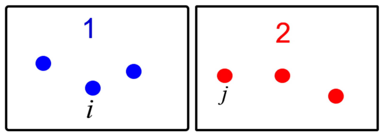
2.1. Lattice Inversion

The accuracy of the interface atomic potential is crucial for studying interface structure and transport properties. Therefore, we employed the Chen–Mobius lattice inversion method [21] to obtain the atomic potential at the Cu/Si interface. This method utilizes the Mobius theorem from number theory combined with crystal structure information to acquire interatomic interaction potential. Particularly, given the current lack of interface atomic potentials, employing lattice inversion methods to obtain them holds significant practical significance. This approach has been successfully applied to various interface scenarios, such as metal/MgO [22], metal/Al2O3 [23], metal/SiC [24], and Ag/Si [25]. Here is a brief overview of the lattice inversion method:
The interfacial adhesive energy can be expressed as follows:
E ( x ) = n = 1 r ( n ) φ ( b ( n ) x ) ,
where x and φ represent the interfacial distance and atomic potential, while r(n) and b(n) denote the coordination number and interatomic distance of the nth nearest neighbor. According to lattice inversion theory, the atomic potential can be written as follows:
φ ( x ) = n = 1 J ( n ) E ( B ( n ) x ) ,
where B(n) is the extended b(n), and J(n) is the inversion coefficient. The set of {B(n)} needs to satisfy the properties of a multiplicative closure, i.e., for any b(n) and b(m), there exists a B(k), such that B ( k ) = b ( m ) × b ( n ) , where m, n, and k are all positive integers. For detailed procedures, please refer to reference [21].
The formula above reveals that acquiring the interfacial adhesion energy and interface structural details is adequate for obtaining the atomic interaction potential between interface atoms. In this paper, the interfacial adhesion energy curve of the Cu/Si interface with varying interface distances was obtained using first-principles methods. Consequently, Equation (2) was utilized to derive the atomic potential between Cu and Si at the interface.
Specifically, the interface potential is obtained as follows:
Step 1: Constructing the interface structure. For example, for the Cu(111)/Si(111) interface, match the 3 × 3 Cu(111) surface with the 2 × 2 Si(111) surface, ensuring that the thickness of the Cu and Si atomic layers perpendicular to the interface exceeds 8 Å. With this, first-principles calculations are performed to compute the static energy of the interface structure at different interface spacings. This gives the interface adhesive energy curve, i.e., E in Equation (2).
Step 2: Determining the nearest-neighbor relationships between the two sides of the interface structure, i.e., r(n) and b(n) in Equation (1). With this, the Mobius inversion is applied to obtain J(n) and B(n), as stated in Equation (2).
Step 3: Obtaining the Cu/Si interface atomic potentials with Equation (2).

2.2. Interface Thermal Conductance

This paper employs equilibrium molecular dynamics combined with the Green–Kubo relation to calculate the interface thermal conductance. The formula for calculating the interface thermal conductance is as follows:
G = 1 A k B T 2 0 Q ( t ) Q ( 0 ) d t ,
where A, kB, and T represent the interface area, Boltzmann constant, and temperature, respectively. Q is the heat flux across the interface, and <Q(t)Q(0)> is the autocorrelation function of the heat flux. The heat flux Q across the interface can be expressed by the following equation:
Q = 1 2 i , j f i j v j f j i v i ,
for the materials I1 and I2, on the two sides of the interface, as shown in Figure 2, where atoms II1 and jI2. fij represent the interaction force between atoms, while vi and vj represent the velocities of atoms i and j, respectively [26]. The factor of 1/2 in the formula takes into account the interaction energy between I1 and I2, with half attributed to I1 and the other half attributed to I2.

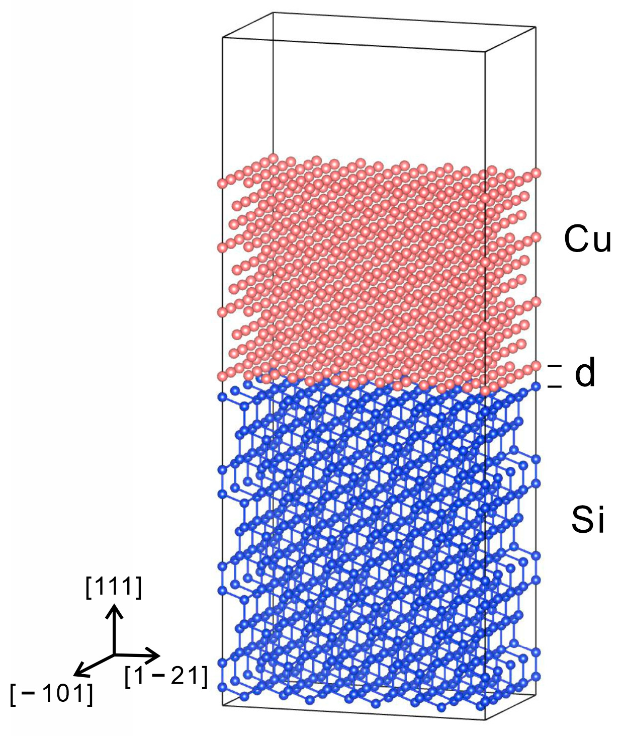
2.3. Computational Details

The adhesive energy was calculated using the first-principles calculation software VASP.5.4.4 [27,28]. The GGA-PBE [29] functional was chosen for the exchange correlation, with a cutoff energy of 400 eV, and an energy convergence criterion of 1 × 10⁻⁶ eV/atom. Calculations were performed only at the Gamma point in reciprocal space. The adhesive energy curve E a d d = E t o t d E t o t , where E t o t represents the system energy at infinite interface distance, is obtained by selecting a cutoff distance of 6 Å to approximate infinite separation.
In this study, the Q was computed using the classic molecular dynamics code LAMMPS [30,31]. The structural model used in the system is shown in Figure 2. Firstly, the model was initially equilibrated using the conjugate gradient method to obtain a minimum energy structure and then relaxed under the Nose–Hoover (NPT) ensemble with zero pressure for 20 ps, and then employed the canonical (NVT) ensemble for 900 ps with a time step of 1 fs. The Cu/Cu potential was described by the embedded atom method (EAM) [32,33]. This EAM potential is a many-body interaction potential primarily used for simulating metal and alloy systems, capable of accurately representing the mechanical properties of metal systems. The Si/Si potential was represented by the Tersoff potential [34]; the Tersoff potential is mainly used to simulate compounds with covalent bonds, accurately reflecting the properties of such bonds. The atomic interaction potentials in bulk materials have been extensively researched, and mature databases have been established, such as the well-known databases created by National Institute of Standards and Technology (NIST). However, due to the complexity of interfaces, there are very few atomic interaction potentials between interfaces. In this paper, the atomic potential between Cu/Si interfaces is obtained through lattice inversion, and the Cu/Si potential parameters using the Morse type listed in Table 1.

3. Results and Discussions

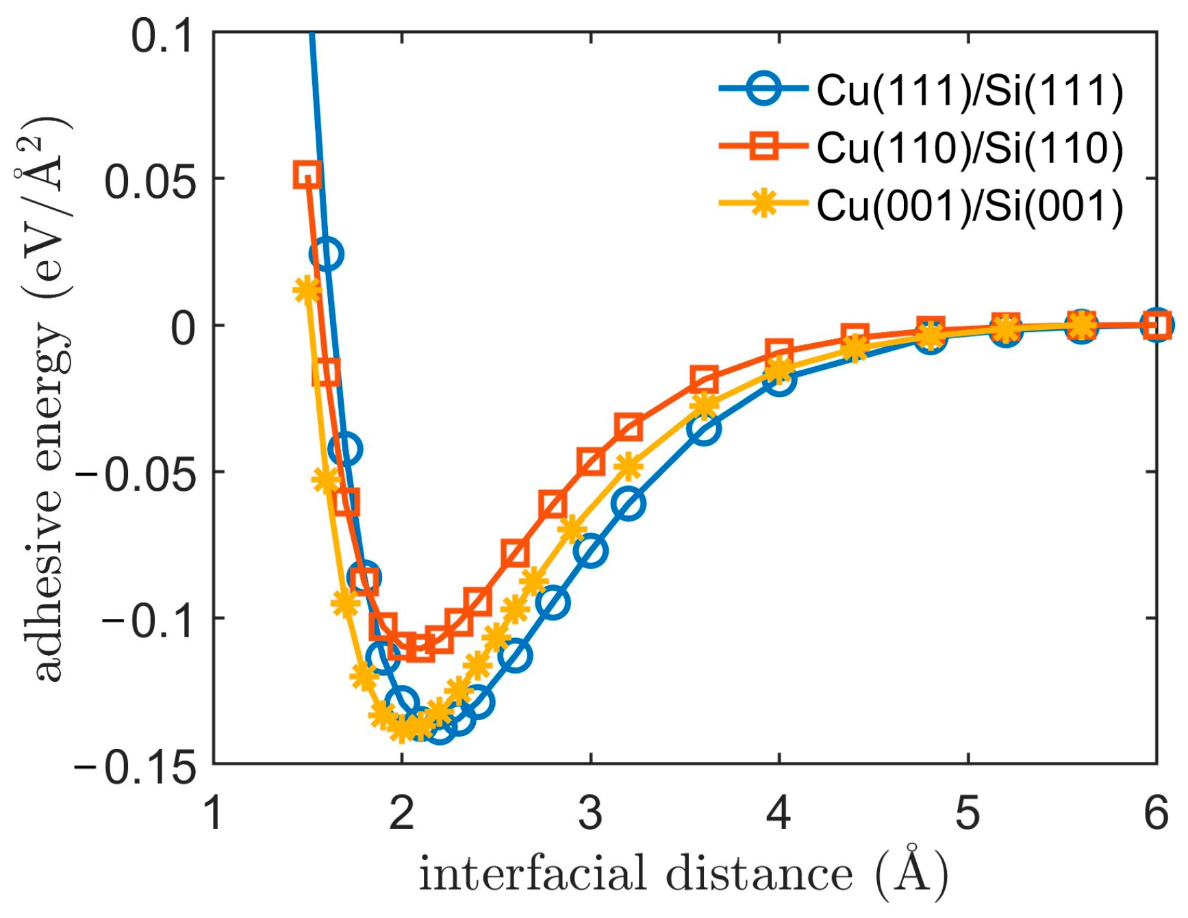
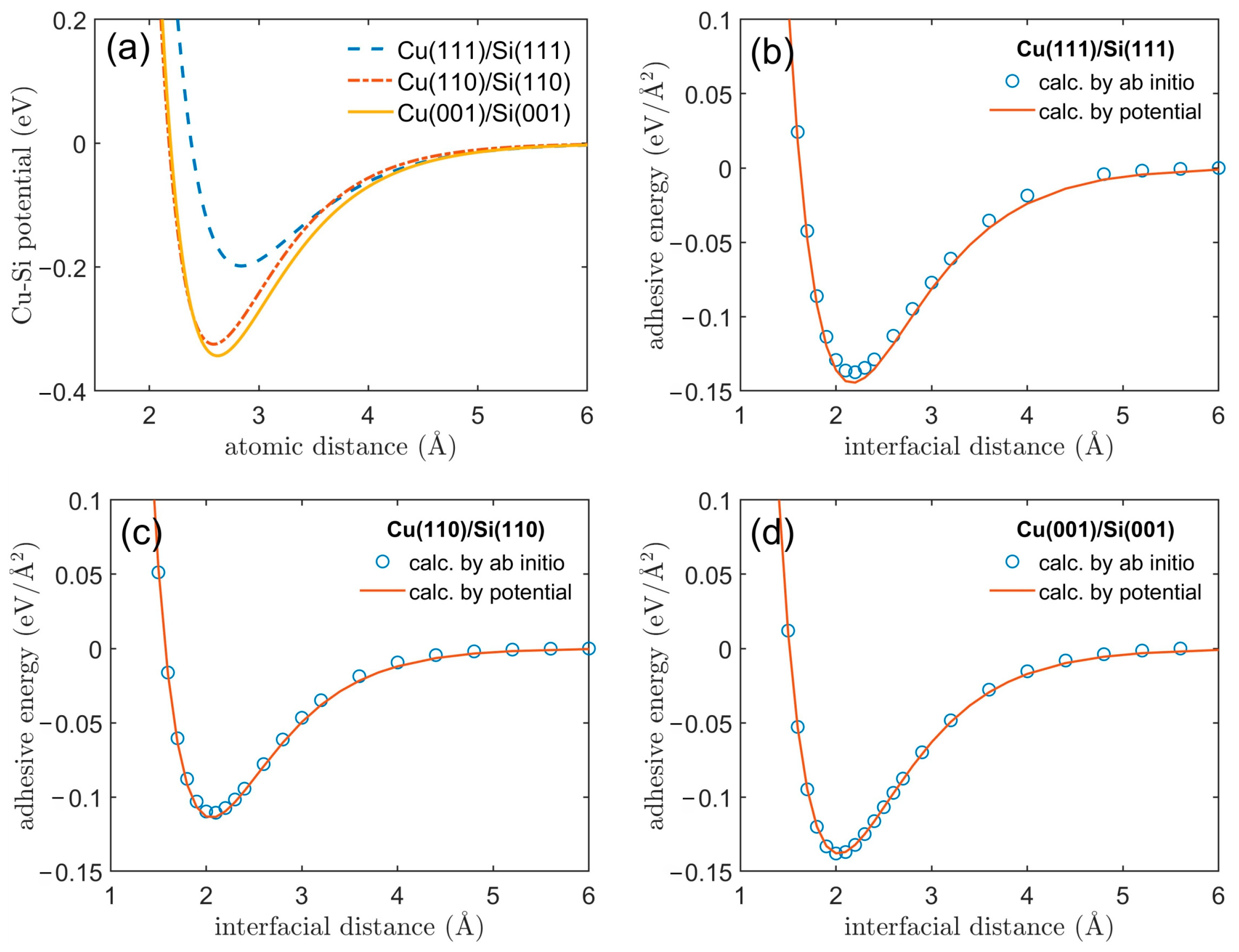
3.1. Adhesive Energy

The lattice constant of Cu in the fcc phase is 3.615 Å, while that of Si in the diamond structure is 5.431 Å. To minimize the lattice mismatch at the interface, we matched six Cu supercells with four Si supercells, resulting in a mismatch of the constructed interface structure of approximately 0.16%, as illustrated in Figure 3.
From Figure 4, it can be observed that the bonding energy of the Cu(111)/Si(111) interface (−0.137 eV/Å2) is close to that of the Cu(001)/Si(001) interface (−0.138 eV/Å2) under the condition of lowest energy, and lower than that of the Cu(110)/Si(110) interface (−0.110 eV/Å2). In contrast to the adhesive energy, the Cu(111)/Si(111) interface spacing (2.2 Å) is the largest under the condition of lowest energy, followed by the Cu(110)/Si(110) interface spacing (2.1 Å), and the smallest is the Cu(001)/Si(001) interface spacing (2.0 Å). This is mainly attributed to two factors: the number of Cu atoms in the interface plane, and the unsaturated chemical bonds of the Si atoms at the interface.
In crystal structures, the number of atoms per unit area is proportional to the interplanar spacing of that plane. Therefore, we can understand the atomic number density within a plane by discussing the interplanar spacing. For the convenience of discussion, the interplanar spacing of the (111) plane, the (110) plane, and the (001) plane are denoted as d111, d110, d001, respectively. For the face-centered cubic phase of Cu, d111 is equal to a / 3 , d110 is equal to a / 8 , and d001 is equal to a / 2 , where a is the lattice constant. The ratio of these interplanar spacing is d 111 : d 110 : d 001 = 8 : 3 : 6 . The crystal structure of Si is the diamond type, composed of two face-centered structures nested within each other, with one displaced relative to the other along the [111] direction. Therefore, the rate of the interplanar spacing of Si is similar to that of Cu. Obviously, the atomic number density is highest on the (111) plane, slightly lower on the (001) plane compared to (111) plane, and lowest on the (110) plane. This trend in variation aligns with the adhesive energies of interface shown in Figure 4.
Figure 4. Curves of the adhesive energies for three Cu/Si interfaces as a function of interfacial distance, computed using first-principles methods.
Metals 14 00453 g004

3.2. Cu/Si Potential

To accurately characterize interface-related properties, this study utilized the lattice inversion method to obtain the Cu/Si potentials for Cu(111)/Si(111), Cu(110)/Si(110), and Cu(001)/Si(001) interfaces, as shown in Figure 5a. For convenience, a Morse function was employed for fitting, and the fitting parameters are detailed in Table 1. The Morse function takes the following form:
φ ( r ) = D 0 e 2 α ( r r 0 ) 2 e α ( r r 0 ) ,
where D 0 , α, and r 0 are the potential parameters. D 0 describes the depth of the potential well, where a larger D 0 indicates a stronger binding energy between atoms. α describes the width of the potential well, with a larger α resulting in a narrower opening of the potential well. Meanwhile, r 0 represents the distance at which interaction force between atoms becomes zero.
From Figure 5a, it is evident that the Cu/Si potentials differ among the three interface conditions. Specifically, the potential well of Cu/Si at the Cu(111)/Si(111) interface is shallower compared to that at the Cu(110)/Si(110) and Cu(001)/Si(001) interfaces. Additionally, the potential well at the Cu(110)/Si(110) interface is slightly shallower than that at the Cu(001)/Si(001) interface. This discrepancy is primarily attributed to interface charge transfer, where a higher number of unsaturated bonds in Si atoms leads to increased charge transfer. For Si with a diamond structure and Cu with a face-centered cubic structure, the (111) planes are densely packed, resulting in weaker interlayer interactions compared to other cases. Consequently, this leads to less charge transfer at the (111) interface, resulting in a weaker Cu/Si potential compared to the other two interface conditions. It is worth noting that the Cu/Si potentials in this paper are smaller than the results in reference [19]. This is mainly because the Cu/Si atomic potential used in this paper is primarily obtained from the interfacial structure’s adhesion energy through lattice inversion methods, while the Cu/Si atomic potential in reference [19] is fitted from the physical properties of bulk materials. The adhesion energy between interfaces is generally much smaller than the bonding energy within bulk materials, resulting in the Cu/Si atomic potential used in this paper being much weaker than that in the literature. This result can be clearly observed from the parameter D 0 in Table 1.
Figure 5. (a) presents the Cu/Si potentials obtained using the lattice inversion method for different Cu/Si interfaces, while (bd) compare the interface adhesion energies calculated by the first-principles method and the Cu/Si potentials.
Metals 14 00453 g005
To validate the reliability of the Cu/Si potentials, we computed the interface adhesion energy for three different interfaces using the derived Cu/Si potential, as depicted in Figure 5b–d. It is evident that the adhesion energies calculated from the Cu/Si potential obtained through inversion closely match the results from first-principles calculations, whether at equilibrium spacing or within compression or stretching ranges. This ensures that the Cu/Si potentials obtained in this study can be applied in molecular dynamics simulations under high-temperature and high-pressure conditions, thereby aiding in further accurate calculations of the thermal conductance of the Cu/Si interface.
Of course, we want to point out that the atomic configuration of the Cu/Si interface is relatively simple such that the lattice inversion can be readily performed. If the configuration of the interface is complex, involving a large number of atoms in the translational unit cell, the lattice inversion may produce non-converged results. On the other hand, similar to other potentials, the lattice inversion potentials also have a limited transferability.

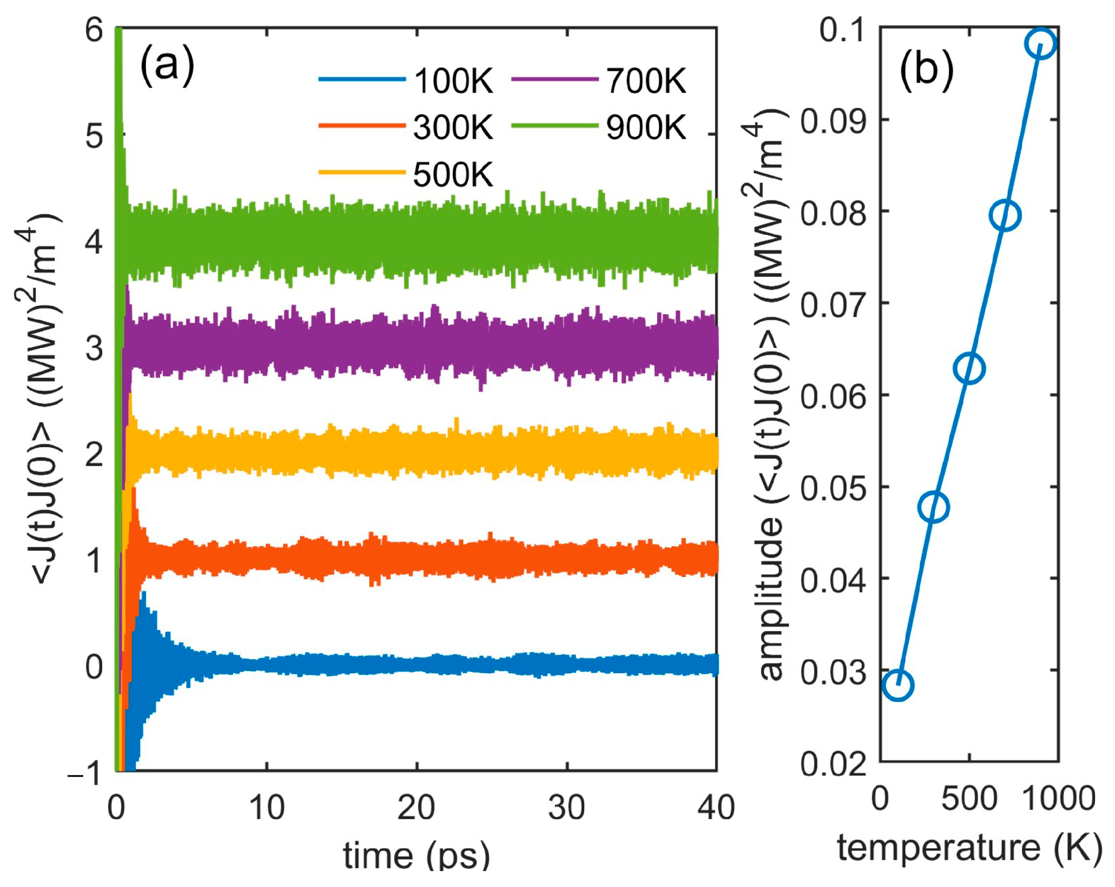
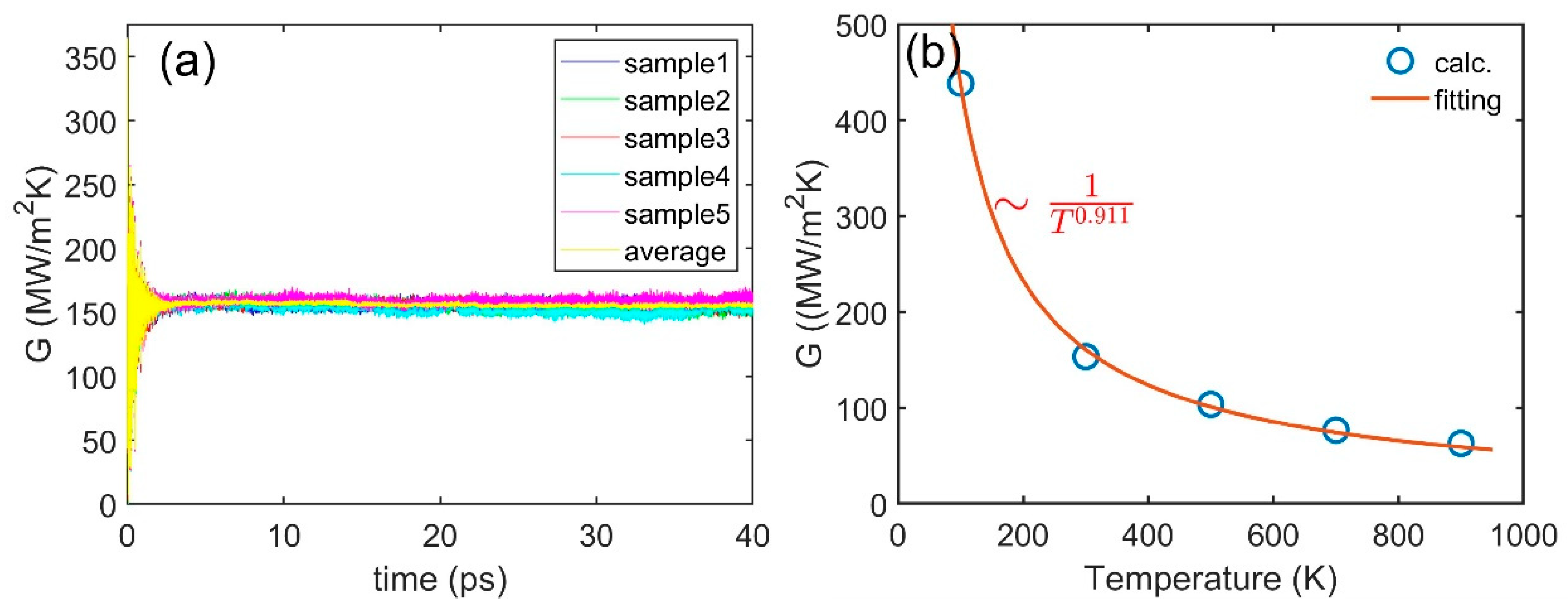
3.3. Interface Thermal Conductance

Equations (3) and (4) indicate that calculating interface thermal conductance requires obtaining the interface heat flux Q. We obtained the velocities and forces of atoms near the interface to calculate the heat flux Q according to Equation (4). Subsequently, the interface thermal conductance was determined using Equation (3).
To understand the relationship between temperature and the interface thermal conductance, we calculated the heat current autocorrelation function at different temperatures, as depicted in Figure 6a. For better comparison, the curves for 300, 500, 700, and 900 K were, respectively, shifted upward by 1 to 4 units. Initially, the heat current autocorrelation function exhibits significant oscillations, followed by gradual convergence. At different temperatures, the convergence rate of the heat current autocorrelation function varies, accelerating with temperature increase. At 100 K, the heat current autocorrelation function reaches convergence near 10 ps, while at 300 K, convergence is achieved in approximately 3 ps. Additionally, the amplitude of oscillations in the converging portion of the heat current autocorrelation function varies with temperature. We calculated the average amplitude of the heat current autocorrelation function within the correlation time range of 10~40 ps, as shown in Figure 6b. It is evident that as temperature increases from 100 to 900 K, the amplitude of the heat current autocorrelation function increases from approximately 0.03 to 0.1 (MW)2/m2, demonstrating a linear relationship with temperature.
The computed thermal conductance of the Cu(111)/Si(111) interface is presented in Figure 7. To minimize errors caused by initial temperature distributions, the calculations were performed five times (as shown in Figure 7a) and averaged. It can be observed that when the correlation time is less than 5 ps, the computed interface thermal conductance has essentially converged, and the fluctuations from multiple calculations are relatively small. From Figure 7b, it is apparent that the thermal conductance of the Cu(111)/Si(111) interface decreases with increasing temperature, roughly inversely proportional to the first power of the temperature. This is mainly caused by two factors: one is the linear increase in the amplitude of the heat current autocorrelation function with temperature, as shown in Figure 6b, and the other is due to the presence of a 1/T2 factor in the calculation of interface thermal conductance in Equation (3). The combined effect of these two factors results in the inverse proportionality of the interface thermal conductance to temperature.
Using the same method, this study calculated the thermal conductivities of the Cu(111)/Si(111), Cu(110)/Si(110), and Cu(001)/Si(001) interfaces at 300 K to be 155, 113, and 192 MW/m2K, respectively. The thermal conductivities of the Cu(111)/Si(111) and Cu(110)/Si(110) interfaces are similar, with both larger than that of the Cu(110)/Si(110) interface. This result is consistent with the interface adhesion energy (Figure 4), indicating that the strength of interface adhesion is one of the main factors influencing interface thermal conductance. From Table 2, it can be observed that the thermal conductance calculated in this study is smaller than the values reported in other studies [19,20]. There are two main reasons for this discrepancy. Firstly, the Cu/Si potential obtained through lattice inversion in this study is weaker than those used in other studies in the literature. Secondly, the Green–Kubo method used in this study does not account for the coupling between electrons and phonons. In reference [19], it was mentioned that in the results of the interface thermal conductance at the Cu/Si interface, the contribution of electron–phonon coupling to the interface thermal conductance accounts for approximately 18% of the total interface thermal conductance. Excluding the effect of electron–phonon coupling, the interface thermal conductance calculated in our work is still lower than that calculated by Lu et al. [19]. The reason for this difference is attributed to the different Cu/Si interfacial potentials. Therefore, this method is not applicable for calculating the interface thermal conductance in conductive systems.

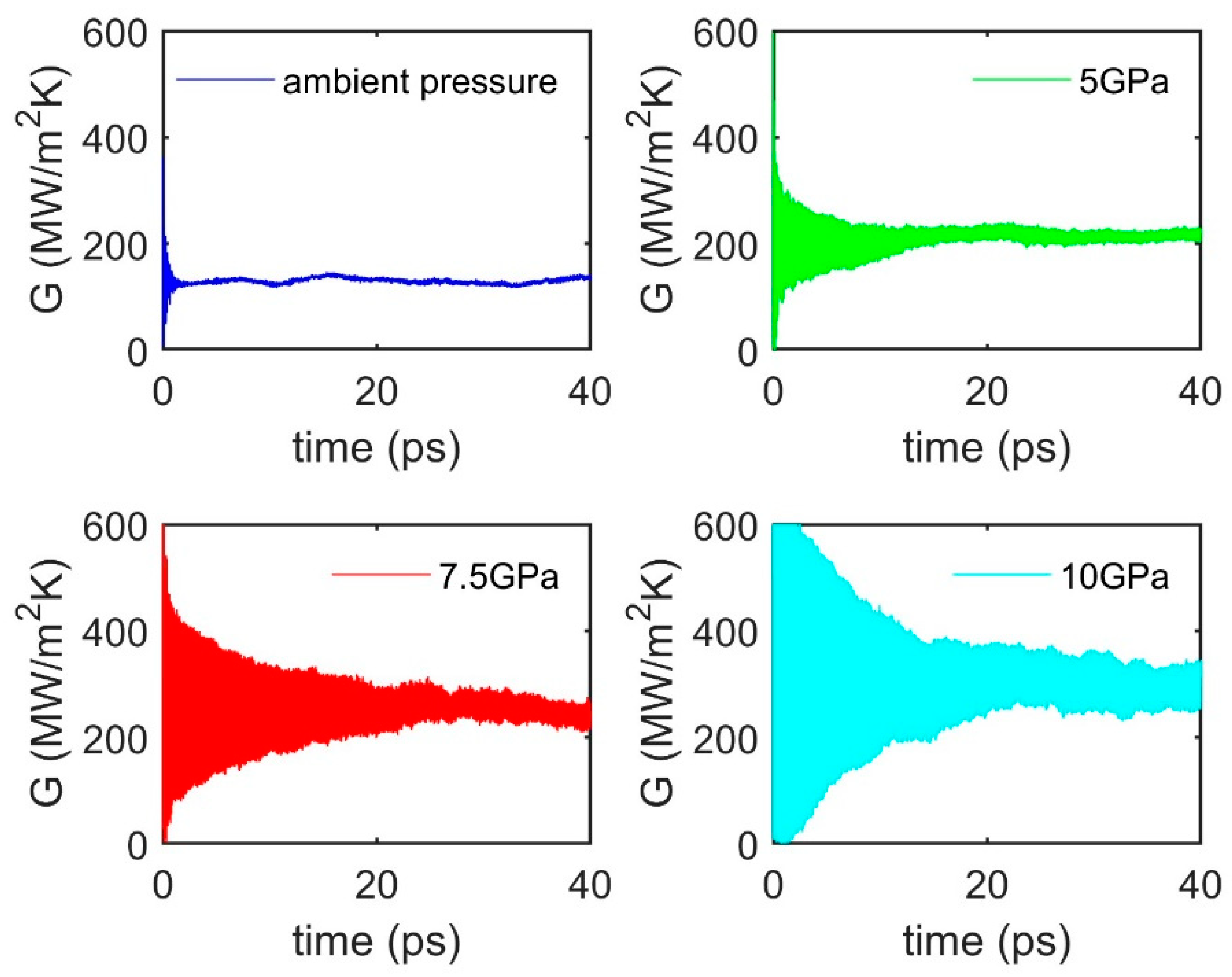
3.4. Pressure Effect

Considering the complexity of material application environments, this paper calculates the variation of interface thermal conductance under pressure perpendicular to the interface. To apply pressure on the system, the molecular dynamics ensemble is chosen as isothermal–isobaric (NPT), with the 300 K temperature and other parameters unchanged. The calculation results are shown in Figure 8. It can be observed that the interface thermal conductance converges fastest under ambient pressure and slows down with increasing pressure. Under 10 GPa, the interface thermal conductance basically converges after 20 ps. The average values of interface thermal conductance between 20~40 ps are listed in Table 2, showing that the interface thermal conductance increases with pressure. When the pressure reaches 10 GPa, the thermal conductance reaches 290 MW/m2K. This is mainly because an increase in pressure reduces the interfacial spacing, leading to an increase in the interaction forces between Cu and Si at the interface. Additionally, when the temperature remains constant, there is not much change in the average velocity of atoms. According to Equation (4), this results in an increase in interfacial heat flux, ultimately leading to an increase in interface thermal conductance.

4. Conclusions

This study conducted first-principles calculations to determine the interface adhesion energy curves for the Cu(111)/Si(111), Cu(110)/Si(110), and Cu(001)/Si(001) interfaces. The results reveal that the adhesion energies of the Cu(111)/Si(111) and Cu(001)/Si(001) interfaces are similar, both exceeding that of the Cu(110)/Si(110) interface. Leveraging the interface adhesion energy curves, this paper obtained Cu/Si interface atomic potentials for the three interface models (Cu(111)/Si(111), Cu(110)/Si(110), and Cu(001)/Si(001)) using lattice inversion methods. In contrast to the interface adhesion energies, the interface potentials obtained by inversion for the Cu(110)/Si(110) and Cu(001)/Si(001) interfaces are close, with their intensities greater than that of the Cu(111)/Si(111) interface. Utilizing the interface potentials obtained by inversion, this study computed the interface thermal conductance of the three interface models. At 300K, the thermal conductance values of the Cu(111)/Si(111) and Cu(110)/Si(110) interfaces are similar, both surpassing that of the Cu(110)/Si(110) interface. The results underscore the correlation between interface thermal conductance and interface adhesion energy. The calculation results show that under pressure applied perpendicular to the interface, the interface thermal conductance increases with increasing pressure. This is primarily attributed to the enhanced interaction between Cu and Si on opposite sides of the interface.
The interface thermal conductance between Cu(001) and Si(001) surfaces is the highest. This suggests a possible direction in the silicon-based device design towards a good heat dissipation performance. Moreover, the findings on the impact of external pressure on interface thermal conductance are also valuable as references for the encapsulation process where external pressure may be exerted to devices. Future research directions include extending this method to other metal–semiconductor interface systems, and even to nanotube–metal interfaces.

Author Contributions

Conceptualization, S.L. and Y.Z.; methodology, H.S.; software, H.L.; validation, W.W., X.H. and D.Z.; formal analysis, S.L., Y.Z. and H.L.; investigation, H.S. and W.W.; resources, Y.Z.; data curation, S.L. and D.Z.; writing—original draft preparation, S.L, Y.Z., H.L. and W.W.; writing—review and editing, H.S., X.H. and D.Z.; visualization, S.L. and Y.Z.; supervision, X.H. and D.Z.; project administration, X.H.; funding acquisition, H.S. and D.Z. All authors have read and agreed to the published version of the manuscript.

Funding

This research was funded by College Students’ Innovative Entrepreneurial Training Plan Program of Henan, grant number 202310478027.

Data Availability Statement

The raw data supporting the conclusions of this article will be made available by the authors on request.

Conflicts of Interest

Authors Shuai Liu, Huijin Li, Weiping Wang and Xiaoyan Hu were employed by the company Information Science Academy of China Electronics Technology Group Cooperation. The remaining authors declare that the re-search was conducted in the absence of any commercial or financial relationships that could be construed as a potential conflict of interest.

References

  1. Li, W.; Li, T.; Tong, Y.; Li, Y.; Wang, H.; Qi, H.; Wang, K.; Wang, H. Reducing Nonradiative Losses of Air-Processed Perovskite Films via Interface Modification for Bright and Efficient Light Emitting Diodes. Adv. Funct. Mater. 2024, 34, 2311133. [Google Scholar] [CrossRef]
  2. Xu, L.; Zhou, L.; Yan, M.; Luo, G.; Yang, D.; Fang, Y. High-Brightness Thermally Evaporated Perovskite Light-Emitting Diodes via Dual-Interface Engineering. Opt. Mater. 2024, 150, 115223. [Google Scholar] [CrossRef]
  3. Lee, W.J.; Sohn, W.B.; Shin, J.C.; Han, I.K.; Kim, T.G.; Kang, J. Growth of InGaAs/InAlAs Superlattices for Strain Balanced Quantum Cascade Lasers by Molecular Beam Epitaxy. J. Cryst. Growth 2023, 614, 127233. [Google Scholar] [CrossRef]
  4. Knipfer, B.; Xu, S.; Kirch, J.D.; Botez, D.; Mawst, L.J. Analysis of Interface Roughness in Strained InGaAs/AlInAs Quantum Cascade Laser Structures (λ∼4.6 μm) by Atom Probe Tomography. J. Cryst. Growth 2022, 583, 126531. [Google Scholar] [CrossRef]
  5. Khan, A.I.; Wu, X.; Perez, C.; Won, B.; Kim, K.; Ramesh, P.; Kwon, H.; Tung, M.C.; Lee, Z.; Oh, I.-K.; et al. Unveiling the Effect of Superlattice Interfaces and Intermixing on Phase Change Memory Performance. Nano Lett. 2022, 22, 6285–6291. [Google Scholar] [CrossRef] [PubMed]
  6. Aryana, K.; Gaskins, J.T.; Nag, J.; Stewart, D.A.; Bai, Z.; Mukhopadhyay, S.; Read, J.C.; Olson, D.H.; Hoglund, E.R.; Howe, J.M.; et al. Interface Controlled Thermal Resistances of Ultra-Thin Chalcogenide-Based Phase Change Memory Devices. Nat. Commun. 2021, 12, 774. [Google Scholar] [CrossRef] [PubMed]
  7. Kim, M.Y.; Park, S.J.; Kim, G.-Y.; Choi, S.-Y.; Jin, H. Designing Efficient Spin Seebeck-Based Thermoelectric Devices via Simultaneous Optimization of Bulk and Interface Properties. Energy Environ. Sci. 2021, 14, 3480–3491. [Google Scholar] [CrossRef]
  8. Wu, W.; Ren, G.-K.; Chen, X.; Liu, Y.; Zhou, Z.; Song, J.; Shi, Y.; Jiang, J.-M.; Lin, Y.-H. Interfacial Advances Yielding High Efficiencies for Thermoelectric Devices. J. Mater. Chem. A 2021, 9, 3209–3230. [Google Scholar] [CrossRef]
  9. Kim, H.; Kwon, Y.; Lim, H.; Kim, J.; Kim, Y.; Yeo, W. Recent Advances in Wearable Sensors and Integrated Functional Devices for Virtual and Augmented Reality Applications. Adv. Funct. Mater. 2021, 31, 2005692. [Google Scholar] [CrossRef]
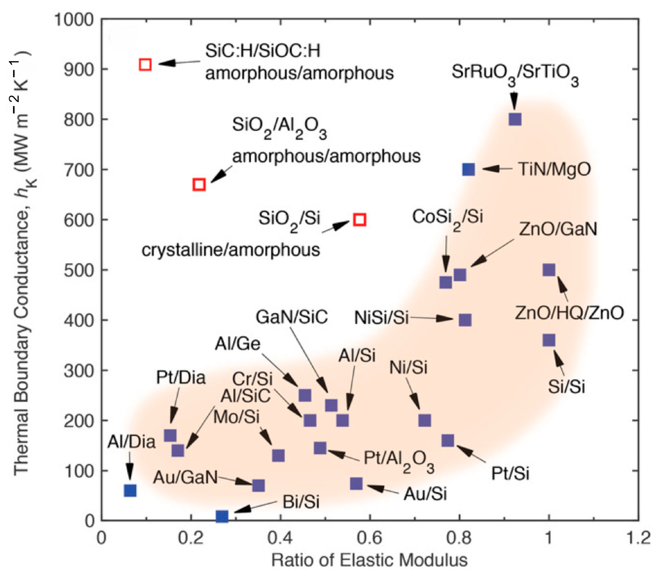
  10. Giri, A.; Hopkins, P.E. A Review of Experimental and Computational Advances in Thermal Boundary Conductance and Nanoscale Thermal Transport across Solid Interfaces. Adv. Funct. Mater. 2020, 30, 1903857. [Google Scholar] [CrossRef]
  11. Findik, F. Laser Cladding and Applications. Sustain. Eng. Innov. 2023, 5, 1–14. [Google Scholar] [CrossRef]
  12. Chen, J. Interfacial Thermal Resistance: Past, Present, and Future. Rev. Mod. Phys. 2022, 94, 25002. [Google Scholar] [CrossRef]
  13. Swartz, E.T.; Pohl, R.O. Thermal Boundary Resistance. Rev. Mod. Phys. 1989, 61, 605–668. [Google Scholar] [CrossRef]
  14. Liang, Z.; Hu, M. Tutorial: Determination of Thermal Boundary Resistance by Molecular Dynamics Simulations. J. Appl. Phys. 2018, 123, 191101. [Google Scholar] [CrossRef]
  15. Little, W.A. The transport of heat between dissimilar solids at low temperatures. Can. J. Phys. 1959, 37, 334–349. [Google Scholar] [CrossRef]
  16. Li, Q.; Liu, F.; Hu, S.; Song, H.; Yang, S.; Jiang, H.; Wang, T.; Koh, Y.K.; Zhao, C.; Kang, F.; et al. Inelastic Phonon Transport across Atomically Sharp Metal/Semiconductor Interfaces. Nat. Commun. 2022, 13, 4901. [Google Scholar] [CrossRef] [PubMed]
  17. Cheaito, R.; Gaskins, J.T.; Caplan, M.E.; Donovan, B.F.; Foley, B.M.; Giri, A.; Duda, J.C.; Szwejkowski, C.J.; Constantin, C.; Brown-Shaklee, H.J.; et al. Thermal Boundary Conductance Accumulation and Interfacial Phonon Transmission: Measurements and Theory. Phys. Rev. B—Condens. Matter Mater. Phys. 2015, 91, 035432. [Google Scholar] [CrossRef]
  18. Stevens, R.J.; Smith, A.N.; Norris, P.M. Measurement of Thermal Boundary Conductance of a Series of Metal-Dielectric Interfaces by the Transient Thermoreflectance Technique. J. Heat Transfer 2005, 127, 315–322. [Google Scholar] [CrossRef]
  19. Lu, Z.; Wang, Y.; Ruan, X. Metal/Dielectric Thermal Interfacial Transport Considering Cross-Interface Electron-Phonon Coupling: Theory, Two-Temperature Molecular Dynamics, and Thermal Circuit. Phys. Rev. B 2016, 93, 064302. [Google Scholar] [CrossRef]
  20. Abs da Cruz, C.; Chantrenne, P.; Gomes de Aguiar Veiga, R.; Perez, M.; Kleber, X. Modified Embedded-Atom Method Interatomic Potential and Interfacial Thermal Conductance of Si-Cu Systems: A Molecular Dynamics Study. J. Appl. Phys. 2013, 113, 023710. [Google Scholar] [CrossRef]
  21. Chen, N. Modified Möbius Inverse Formula and Its Applications in Physics. Phys. Rev. Lett. 1990, 64, 1193–1195. [Google Scholar] [CrossRef] [PubMed]
  22. Long, Y.; Chen, N.X.; Zhang, W.Q. Pair Potentials for a Metal–Ceramic Interface by Inversion of Adhesive Energy. J. Phys. Condens. Matter 2005, 17, 2045–2058. [Google Scholar] [CrossRef]
  23. Long, Y.; Chen, N.X. Pair Potential Approach for Metal/Al2O3 Interface. J. Phys. Condens. Matter 2007, 19, 196216. [Google Scholar] [CrossRef]
  24. Zhao, H.; Chen, N.; Long, Y. Interfacial Potentials for Al/SiC(111). J. Phys. Condens. Matter 2009, 21, 225002. [Google Scholar] [CrossRef] [PubMed]
  25. Liu, Y.-Q.; Song, H.-Q.; Shen, J. Interfacial Potential Approach for Ag/Si(111) Interface. Mod. Phys. Lett. B 2016, 30, 1650104. [Google Scholar] [CrossRef]
  26. Domingues, G.; Volz, S.; Joulain, K.; Greffet, J. Heat Transfer between Two Nanoparticles Through Near Field Interaction. Phys. Rev. Lett. 2005, 94, 085901. [Google Scholar] [CrossRef] [PubMed]
  27. Kresse, G.; Furthmüller, J. Efficient Iterative Schemes for Ab Initio Total-Energy Calculations Using a Plane-Wave Basis Set. Phys. Rev. B 1996, 54, 11169–11186. [Google Scholar] [CrossRef] [PubMed]
  28. Kresse, G.; Furthmüller, J. Efficiency of Ab-Initio Total Energy Calculations for Metals and Semiconductors Using a Plane-Wave Basis Set. Comput. Mater. Sci. 1996, 6, 15–50. [Google Scholar] [CrossRef]
  29. Perdew, J.P.; Burke, K.; Ernzerhof, M. Generalized Gradient Approximation Made Simple. Phys. Rev. Lett. 1996, 77, 3865–3868. [Google Scholar] [CrossRef]
  30. Plimpton, S. Fast Parallel Algorithms for Short-Range Molecular Dynamics. J. Comput. Phys. 1995, 117, 1–19. [Google Scholar] [CrossRef]
  31. Thompson, A.P.; Aktulga, H.M.; Berger, R.; Bolintineanu, D.S.; Brown, W.M.; Crozier, P.S.; in ’t Veld, P.J.; Kohlmeyer, A.; Moore, S.G.; Nguyen, T.D.; et al. LAMMPS—A Flexible Simulation Tool for Particle-Based Materials Modeling at the Atomic, Meso, and Continuum Scales. Comput. Phys. Commun. 2022, 271, 108171. [Google Scholar] [CrossRef]
  32. Johnson, R.A. Alloy Models with the Embedded-Atom Method. Phys. Rev. B 1989, 39, 12554–12559. [Google Scholar] [CrossRef] [PubMed]
  33. Zhou, X.W.; Johnson, R.A.; Wadley, H.N.G. Misfit-Energy-Increasing Dislocations in Vapor-Deposited CoFe/NiFe Multilayers. Phys. Rev. B 2004, 69, 144113. [Google Scholar] [CrossRef]
  34. Tersoff, J. Modeling Solid-State Chemistry: Interatomic Potentials for Multicomponent Systems. Phys. Rev. B 1989, 39, 5566–5568. [Google Scholar] [CrossRef] [PubMed]
Figure 1. Experimentally measured thermal boundary conductance versus the ratio of the elastic moduli of the two constituent materials [10].
Metals 14 00453 g001
Figure 2. Schematic of the interface structure.
Metals 14 00453 g002
Figure 3. Cu(111)/Si(111) interface structure, with six unit cells of Cu matched with four unit cells of Si. The thickness of Cu is 18.8 Å (10 atomic layers), while Si has a thickness of 29.0 Å (10 double atomic layers). d represents the interfacial distance, and the vacuum layer is about 15 Å thick.
Metals 14 00453 g003
Figure 6. The variation curve of the heat current autocorrelation function over time (a) and the average amplitude between 10~40 ps (b).
Metals 14 00453 g006
Figure 7. (a) illustrates the change in thermal conductance of the Cu(111)/Si(111) interface with correlation time at 300 K, and (b) shows its variation with temperature.
Metals 14 00453 g007
Figure 8. Interface thermal conductance of Cu(111)/Si(111) interface under different pressures at 300 K temperature.
Metals 14 00453 g008
Table 1. Parameters of Cu/Si potential obtained by the lattice inversion method and other references, with the potential function in Morse form.
Interface ModelD0 (eV)αr0 (Å)
Cu(111)/Si(111)0.19831.51882.8395
Cu(110)/Si(110)0.32471.70092.5873
Cu(001)/Si(001)0.34341.61542.6225
Cu/Si [19]0.91.113.15
Table 2. Summary of the calculated interface thermal conductance of the Cu/Si interface in this work and other references.
Interface ModelTemperature (K)Pressure (GPa)G (MW/m2K)
Cu/Si [19]300-436
Cu/Si [20]300-234–263
Cu(110)/Si(110)3000113
Cu(001)/Si(001)3000192
Cu(111)/Si(111)1000438
3000153
5000101
700074
900059
300Ambient125
3005213
3007.5248
30010290
Disclaimer/Publisher’s Note: The statements, opinions and data contained in all publications are solely those of the individual author(s) and contributor(s) and not of MDPI and/or the editor(s). MDPI and/or the editor(s) disclaim responsibility for any injury to people or property resulting from any ideas, methods, instructions or products referred to in the content.

