Article

Influence of the Material Production Route on the Material Properties and the Machinability of the Lead-Free Copper-Zinc-Alloy CuZn40 (CW509L)

1
Manufacturing Technology Institute MTI, RWTH Aachen University, Campus Boulevard 30, 52074 Aachen, Germany
2
Fraunhofer Institute for Production Technology IPT, Steinbachstr. 17, 52074 Aachen, Germany
*
Author to whom correspondence should be addressed.
Metals 2024, 14(7), 747; https://doi.org/10.3390/met14070747
Submission received: 29 April 2024 / Revised: 18 June 2024 / Accepted: 20 June 2024 / Published: 25 June 2024
(This article belongs to the Special Issue Advances in Copper, Copper Alloys and Their Processing)

Abstract

:
To improve the machinability properties of CuZn-alloys, these are alloyed with the element lead. Due to its toxicity, a variety of legislative initiatives aim to reduce the lead content in CuZn-alloys, which results in critical machinability problems and a reduction in the productivity of machining processes. Basically, there are two ways to solve the critical machinability problems when machining lead-free CuZn-alloys: optimizing the machinability of lead-free materials on the material side or adapting the processes and the respective process parameters. In this study, the focus is on material-side machinability optimization by investigating the influence of a targeted variation in the process chain in the material production route. To evaluate the influence of the material production route, the brass alloy CuZn40 (CW509L) was produced in four variants by varying the degree of work hardening and the use of heat treatments, and all four variants were evaluated in terms of their machinability. To evaluate the machinability, the cutting force components, the chip temperature, the chip formation, and the chip shape were analyzed. Clear influences of the material production route were identified, particularly with regard to the chip formation mechanisms and the resulting chip shape.

1. Introduction

Copper-based materials have historically been of great technical relevance for several millennia. Due to the global structural change in the areas of digitalization, energy supply, and mobility, the importance of copper-based materials is constantly increasing. This applies in particular to CuZn-alloys (brass), which are characterized by very good electrical conductivity, good adjustability of the mechanical properties, and generally good machining properties. As machining is one of the most important value-added processes for many brass products, the machinability of these materials is highly relevant. In order to achieve good machining properties, the element lead with mass contents of up to mPb = 4% was added to CuZn-alloys in the past. Since lead is non-soluble in brass, it segregates as small globules around the grain boundaries. The lead segregations elongate to form flake-like structures that act as crack initiation points and thus lead to chip breaking [1]. The cost-effective and efficient machinability of these materials is offset by the harmful effects of the element lead on the environment and health. For this reason, the maximum permissible lead content in metallic alloys has been increasingly reduced in recent years by statutory regulations. For copper alloys, there is still an exemption, which allows the use of lead as an alloying element in CuZn-alloys. Due to various regulations in the EU, for many applications, these exemptions are expected to expire in 2026. For this reason, the affected industries will soon be dependent on lead-free alternative alloys with comparable application and machinability properties. While lead-free CuZn-alloys generally retain outstanding application properties, their machinability and also their cost-effectiveness in mass production can be classified as significantly worse. Non-breaking, long chips, high process forces, and higher tool wear are the results [1,2,3], which is why more and more approaches are being researched to optimize the machinability of lead-free CuZn-alloys. However, it is not known how the targeted variation in the mechanical properties, microstructure, and chemical composition affects the chip formation of lead-free CuZn-alloys and which mechanisms of action underlie the process. Knowledge of these underlying cause-and-effect relationships would enable a more targeted design of lead-free alternative materials with better machinability properties.
In the past, a large number of studies have already been carried out to optimize the machinability of lead-free CuZn-alloys. While machinability depends on the properties of the material as well as the selected process parameters and process boundary conditions, most studies have focused on optimizing machinability on the process side. For example, there is a large number of research papers that have dealt with the tool and process design for turning, drilling, or milling of lead-free CuZn-alloys [2,4,5,6,7,8,9,10,11,12,13,14]. Consequently, there is a broad knowledge of how to adapt tools and processes for the machining of existing lead-free CuZn-alloys. A major challenge is the material-side machinability optimization of lead-free CuZn-alloys, where the potential has so far been insufficiently exploited. In the past, scientific approaches to substituting lead with other elements that do not have the same harmful effects on health or the environment as lead have been researched. The elements investigated include bismuth [15,16], graphite [17,18], or silicon [2,19,20,21]. So far, silicon has established itself as the only industrially relevant lead alternative with the aim of improving machinability. However, the use of silicon as an alloying element results in a drastic reduction in electrical conductivity and is therefore unsuitable for electrical applications. In machining, the use of Si-containing CuZn-alloys is associated with increased tool wear due to the highly abrasive κ-phase [2]. In addition, the influence of mechanical material properties and the microstructural properties of lead-free CuZn-alloys on machinability was investigated in the past [5,22,23,24,25,26,27]. Hofmann et al. used low lead CuZn-alloys to investigate whether a reduced mass fraction of lead can be compensated for and whether satisfactory chip-breaking behavior can be achieved by adjusting certain material properties (strength, ductility, and microstructure) [28]. To this end, the authors systematically varied the lead content and the strength condition of the investigated materials and evaluated the chip-breaking properties in the form of the chip space number RZ on the basis of tests during external longitudinal turning. The investigations showed that, in addition to the lead content, the microstructure also has an influence on chip breaking and the resulting chip space number. On average, a fine needle-like α-phase led to poorer chip-breaking behavior. However, more profound correlations between material properties and machinability could not be determined [28]. For this purpose, it is necessary to carry out a systematic variation of the material production route and to analyze the underlying chip formation mechanisms as a function of the material properties.
In the present work, a systematic variation of material properties of lead-free CuZn-alloys on chip formation is investigated in cooperation with the Innovation Network Copper Processing (IKB). The long-term goal is to enable a targeted and economical material design of lead-free CuZn-alloys by identifying the underlying mechanisms of action. This study should contribute to the identification of mechanisms of action between microstructure formation and machinability and thus contribute significantly to this goal. The focus of the work is on the influence analysis of different material characteristics on machinability, which were adjusted by a systematic variation of the material product production route. The extent to which a variation of heat treatment and work hardening in different stages affects the material properties and the machinability is examined in detail.

2. Materials and Methods

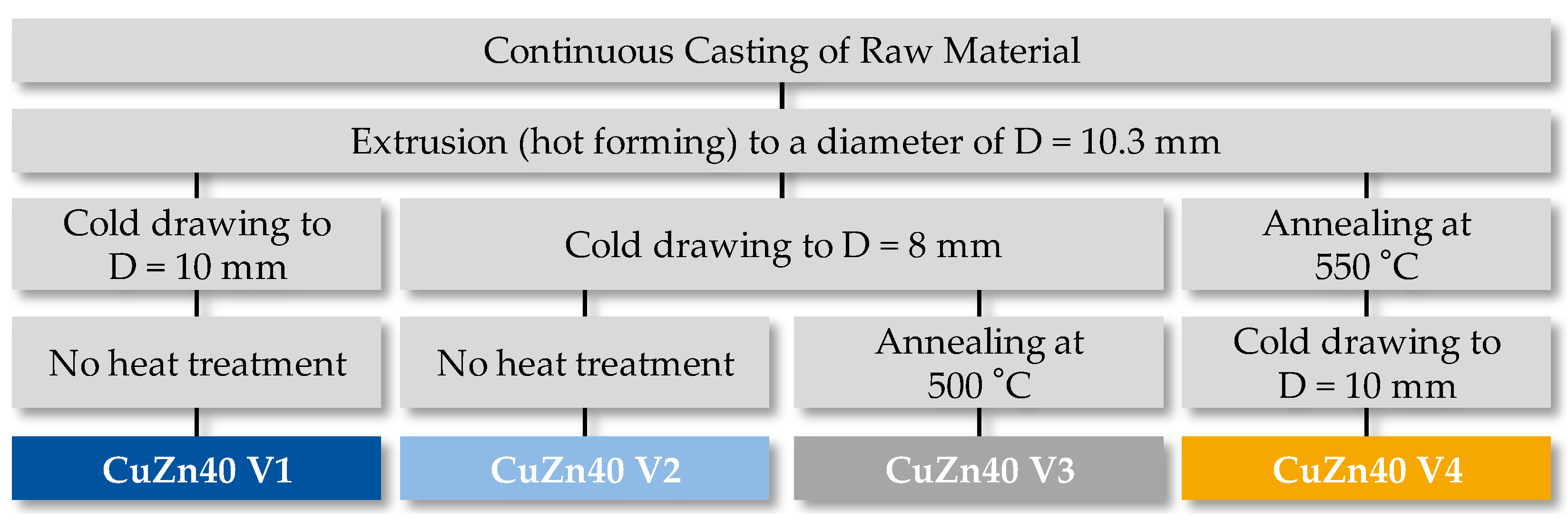
2.1. Investigated Materials

In this study, the lead-free alloy CuZn40 (CW509L) with varying material production routes was investigated. CuZn40 is a relevant lead-free alternative alloy for the electrical industry in particular, as it represents a good compromise between cold formability and machinability. Nevertheless, the machinability is not good enough to realize economic mass production and is clearly inferior to the lead-containing reference alloy CuZn39Pb3 in terms of chip shape and resulting process reliability. A targeted design of the material and microstructure properties, therefore, has the potential to further improve machinability [26]. In order to identify this potential, the process parameters in the work hardening process and heat treatment were specifically varied while maintaining the same chemistry, resulting in different material and microstructural properties [26,29]. Figure 1 provides an overview of the different process routes and the four resulting material variants.
The materials investigated in this work were all initially cast using a conventional continuous casting process. The cast slabs were subsequently extruded (hot forming) into bars with a uniform diameter of D = 10.3 mm. Up to this process step, all the bars examined, which all came from the same casting, were treated in the same way. It can, therefore, be assumed that the entire bar material was identical, disregarding inhomogeneities and fluctuations in the casting process. The material was then fed into different process routes, which ultimately produced four different material variants. The first material variant V1 was cold worked from D = 10.3 mm to DV1 = 10 mm after the extrusion process. This allowed a low degree of work hardening to be achieved. This was followed by no further processing steps. In contrast to the first variant, the second material variant V2 was drawn from D = 10.3 mm to DV2 = 8 mm. As a result, a significantly higher degree of work hardening was contributed compared to the first variant. This was followed by no further processing step. The third material variant V3 underwent the same high degree of work hardening as V2 from D = 10.3 mm to DV3 = 8 mm. A single-stage heat treatment of the bar material was then carried out. For this, the material was annealed for tannealing = 120 min at Tannealing = 500 °C. Cooling took place in cooling chambers with high convection in air. The last material variant V4 also underwent a heat treatment process, but this was carried out directly after the extrusion process. For this, the extruded material was annealed for tannealing = 120 min at Tannealing = 550 °C and then cooled in cooling chambers with high convection in air, as in V3. Following the heat treatment, the cooled material was drawn from D = 10.3 mm to DV4 = 10 mm, whereby the same degree of cold work hardening was achieved as in V1. With the described variations, the two most relevant material production processes after casting were varied within the industrially relevant range. In the course of work hardening, the technically relevant lowest and highest work hardening level was chosen. To investigate the influence of heat treatment, a combination of temperature and time was initially selected that promised a strong transformation in the microstructure while retaining the technically relevant mechanical properties. In addition, the influence of the heat treatment before and after work hardening was investigated. The four material variants were extensively characterized in order to identify the influence of the variation in the material production route and to define the material input condition for the machining process. The material characterization included analyzing the chemical composition, mechanical material parameters, and microstructural properties. The results of the material characterization are shown below.

2.1.1. Chemical Composition

The chemical composition was identical for all 4 material variants due to the identical casting process and is shown in Table 1.

2.1.2. Mechanical Material Properties

Due to the described variation of the semi-finished product production route during cold drawing and heat treatment, significant differences in the microstructure and mechanical properties of the four material variants V1–V4 were to be expected. To record the mechanical differences, material testing methods relevant to machining were selected and carried out. The selected test methods included the tensile test according to DIN EN ISO 6892-1 [30], the compression test according to DIN50106 [31], the Vickers hardness test according to DIN EN ISO 6507-1 [32], the Vickers microhardness test according to DIN EN ISO 14577-1 [33], the impact test according to DIN EN ISO 148-1 [34], and the friction test under machining conditions according to Puls [35]. Table 2 shows the results of the mechanical material parameters.
The highest strength (Rp0.2 = 585 MPa, Rm = 617 MPa) and at the same time the lowest ductility (A = 13.2%) can be found in V2. This is due to the highest work hardening in the production of the material. V3 has the lowest strength and highest ductility (Rp0.2 = 201 MPa and Rm = 433 MPa and A = 46.1%), as it was heat-treated again after work hardening. The materials V1 and V4 are classified between V2 and V3 in terms of their strength and ductility and do not differ significantly from each other in this respect. A qualitatively similar behavior between the material variants can be seen in the hardness measurements and the compression tests. In terms of notched impact strength, the material variants exhibited different behavior. V2 has the lowest notched impact strength (ak,V2 = 8 J/cm2), which was to be expected due to the high work hardening. V4 also had a relatively low notched impact strength (ak,V4 = 9 J/cm2), although the sample only underwent minor work hardening. This is possibly due to microstructural changes in the course of the upstream annealing and is confirmed by the fact that V1, which underwent the same work hardening as V4, but no annealing, has a significantly higher notched impact strength (ak,V1 = 12.6 J/cm2). The highest notched impact strength was exhibited by V3, which was heat-treated after work hardening, with ak,V3 = 14.4 J/cm2. In addition to the conventional mechanical material parameters, the tribological relationships in the contact zone between the material and the cutting material are highly relevant for chip formation and tool wear and, therefore, represent a material parameter relevant for machining [35]. In previous work on the analysis of the frictional behavior between material and cutting material, a methodology was developed at the MTI (previous WZL) that makes it possible to record the tribological relationships under machining-like conditions [35,36,37]. In this work, this method was transferred for use with brass materials and used to determine the coefficient of friction as a function of relative speed and temperature. As expected, the temperature in the contact zone increases with increasing relative speed for all materials and the resulting coefficient of friction µ decreases. When looking at the coefficients of friction for the four material variants, strong differences are noticeable. V3 has the highest coefficient of friction (0.36 ≤ µV4 ≤ 0.50), while V2 has the lowest coefficient of friction (0.21 ≤ µV2 ≤ 0.28). The materials V1 and V4 are in between and have an almost identical coefficient of friction. Therefore, the coefficient of friction µ correlates strongly with the toughness of the material in the form of the elongation at break A.

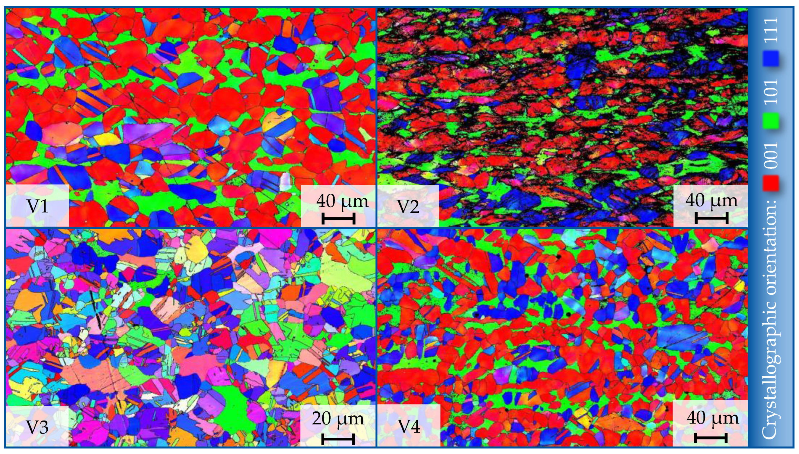
2.1.3. Characteristics of the Material Microstructure

In order to obtain a comprehensive picture of the test materials examined, a detailed microstructure analysis was carried out in addition to the extensive investigations of the mechanical characteristics. This consisted of a qualitative analysis of light microscopic cross-sections which was carried out with a light microscope type Zeiss M2M (Carl Zeiss AG, Oberkochen, Germany) and an in-depth Electron Backscatter Diffraction (EBSD) analysis carried out with a scanning electron microscope type Zeiss Sigma VP 500 (Carl Zeiss AG). The additional observation of the microstructure made it possible to correlate the causes of the material properties introduced in the material production route in terms of mechanical and structural properties and thus to draw better conclusions about the fundamental cause–effect relationships of machinability, especially chip formation. The influence of the degree of work hardening on the microstructure can be seen from the longitudinal metallographic crosssections examined (Figure 2). While the material variants V1 and V4 exhibited a predominantly globulitic microstructure, V2 and V3 exhibited an elongated ß-phase with an orientation in the longitudinal direction of the bar. These more solidified grains of the ß-phase might lead to better segmentation and chip-breaking behavior [38]. Further V2 and V3 in particular again had a significantly finer-grained microstructure, which can also be attributed to work hardening. V3 underwent recrystallization in the subsequent heat treatment, which could be seen in the blurred grain boundaries. The influence of annealing at the end of the production route of V3 becomes even clearer when looking at the crystallographic orientation of the grains in the EBSD (Figure 3). While the variants V1, V2, and V4 showed a crystallographic direction in 0-0-1 (anisotropy), the orientation of the grains in V3 was almost random. This is due to the recrystallization triggered by the annealing, which dissolves the grain orientations introduced by the cold drawing process. The effect of annealing cannot be seen in V4, as the cold deformation was only introduced after annealing. On a crystallographic level, this also explains the difference in strength and ductility between the material variants. A clear crystallographic preference is the result of the movement of defects within the crystal lattice on slip systems. This movement leads to a crystallographic reorientation of the grains in the deformed sample so that the affected grains all have the same crystallographic orientation. This uniform movement results in a higher resistance to dislocations. The result is higher strength and lower ductility, which is particularly evident in variant V2. The resulting defects are also visible in the EBSD analysis, particularly in the heavily deformed V2. Due to the strong deformation and the formation of defects, the EBSD determines zero solutions, which can be seen as black defects in the EBSD image.
In addition to the qualitative evaluation of the microstructure, the EBSD analysis was used to do numerical calculations of relevant microstructure-specific parameters. The focus was on the size and shape of the individual grains. Within the scope of this work, the phase fractions were first determined and the mean grain area A, the equivalent diameter d, and the grain shape in the form of the aspect ratio were measured separately for both phases, Table 3. A higher proportion of α-phase was detected in all material variants (72% ≤ φα ≤ 88%). While the two variants with low work hardening (V1 and V4) showed an almost identical proportion of β-phase of φβ,V4 = 18% and φβ,V1 = 19%, respectively, this varied more strongly in the highly work-hardened variants V2 and V3. The lowest overall proportion of β-phase was detected in V3 with φβ,V3 = 12%, while the non-heat-treated variant V2 had the highest proportion of brittle β-phase in terms of area with φβ,V4 = 28%. The average grain area ak indicates the average value of all measured grains of each phase. As the grains have different shapes, the total grain area is used rather than the diameter. Two aspects in particular became apparent here: both work hardening and heat treatment had a grain refining effect. Looking first at the non-heat-treated material variants V1 and V2, it can be seen that the more work-hardened variant V2 only took up about half the grain area of the less work-hardened variant V1 in both phases. The same behavior was also observed for the two heat-treated test materials V3 and V4, where the more work-hardened variant V3 had a significantly smaller average grain area than V4. Comparable results were also obtained by calculating the respective equivalent diameter d. The grain aspect ratio b/h between the width and height of this equivalent ellipse can be used to indicate whether the respective phases are more acicular or globulitic. It was shown that there were no major differences in the aspect ratio of the equivalent ellipse. The morphology of the different test material variants was, therefore, comparable for all variants. Basically, the β-phase had a higher aspect ratio and was less globulitic in shape and more elongated compared to the α-phase. This corresponds to the observations from the micrographs (Figure 2).

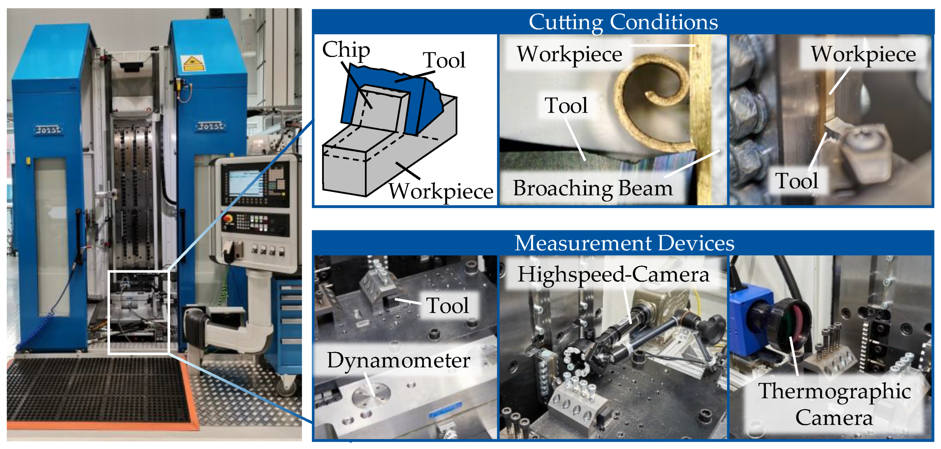
2.2. Experimental Setup

In order to enable a more in-depth analysis of the underlying chip formation mechanisms and to realize a broad transferability of the results, an analogy cutting process with orthogonal cutting conditions was chosen for the investigations. Accordingly, the experimental investigations were carried out on a test rig with translational kinematics. The corresponding test rig for the investigations in this paper was set up on a vertical broaching machine of the type FORST RASX 8X2200X600 M/CNC (Forst Technologie GmbH & Co. KG, Solingen, Switzerland) (Figure 4). Appropriate measuring technology was installed on the machine table for an in-depth analysis of the machinability. This included a 3-component dynamometer type KISTLER 9257 B (Kistler Instrumente AG, Winterthur, Switzerland) with charge amplifier, a high-speed camera with ring light type Vision Research Phantom v7.3 (Vision Research, Wayne, NJ, USA), and a thermographic camera type Teledyne Flir sc7500 (Teledyne FLIR, Santa Barbara, CA, USA). While the tool was clamped in an NSL2525M3 (Kennametal, Pittsburgh, PA, USA) top-notch tool holder with a cage on the dynamometer, the cameras were positioned on the machine table in such a way that they were focused on the cutting edge of the tool. The relative movement between the tool and workpiece required for machining was realized by the vertically movable broaching beam of the machine, in which the workpiece was clamped in the form of a small plate. The test plates were cut out of the bar material using erosion and measured 3 mm × 7.6 mm × 8 mm.

2.3. Experimental Design

Lead-free copper materials are used in a wide range of applications. Accordingly, small components such as electrical connectors with component diameters of D = 0.3 mm and larger sanitary components with diameters of up to D = 50 mm have to be machined. Due to the massive differences in the size of the machined components, the process parameters used also vary over a wide parameter range. Therefore, an experimental design was developed that covers a wide range of industrially relevant parameters. To realize this and also to analyze interactions between material and process parameters, a total of three complete series of tests with a total of 164 test points were carried out (Table 4).
The first test series was used to investigate the influence of the material production route when varying the depth of cut respectively the feed rate. In addition to the feed rate and the material, all process parameters were kept the same and the feed rate was varied in eleven steps between 0.01 mm ≤ f ≤ 0.5 mm. In the second series of tests, the focus was on varying the cutting speed vc. This was varied in six steps in a range of 25 m/min ≤ vc ≤ 150 m/min. In order to be able to additionally investigate interactions in the extreme parameter ranges, a min–max variation was carried out in test series 3. Here, the feed rate was varied with the extreme values f = 0.01 mm and f = 0.5 mm from test series 1, and the cutting speed with the extreme values vc = 25 m/min and vc = 150 m/min in a full-factorial manner. All other parameters and process boundary conditions such as machine, tool holder, tool geometry, and the absence of cooling lubricant were kept constant throughout the whole tests, and in all three test series, each test point was repeated once. In each test point of the three test series, cutting force components and chip temperature were measured, high-speed videos of chip formation were recorded, and the resulting chips were collected.

3. Results and Discussion

To analyze the influence of the material manufacturing route on machinability, various evaluation parameters were recorded in the machining tests (Section 2.2 and Section 2.3) with which machinability can be evaluated. The evaluation parameters included the cutting force components (Section 3.1), the chip temperature (Section 3.2), as well as the underlying chip formation mechanisms and the resulting chip shape (Section 3.3). The focus of the evaluation was on the critical evaluation parameter of chip formation and chip shape for the machining of lead-free CuZn-alloys. To analyze the influence of the material manufacturing route on the evaluation criteria, a main effect diagram for each evaluation criterion was determined in which the influence of the material was averaged over all parameter ranges (Figure 5, Figure 6, Figure 7, Figure 8, Figure 9 and Figure 10). This enabled the possibility to statistically describe and analyze the influence of a single parameter (in this case the material) over the entire parameter range. Further results of chip analysis for individual test points and for the variation in the process parameters were also analyzed and are given in Appendix A (Figure A1, Figure A2, Figure A3, Figure A4 and Figure A5). The influences of the material production route on the three evaluation variables are described and discussed below.

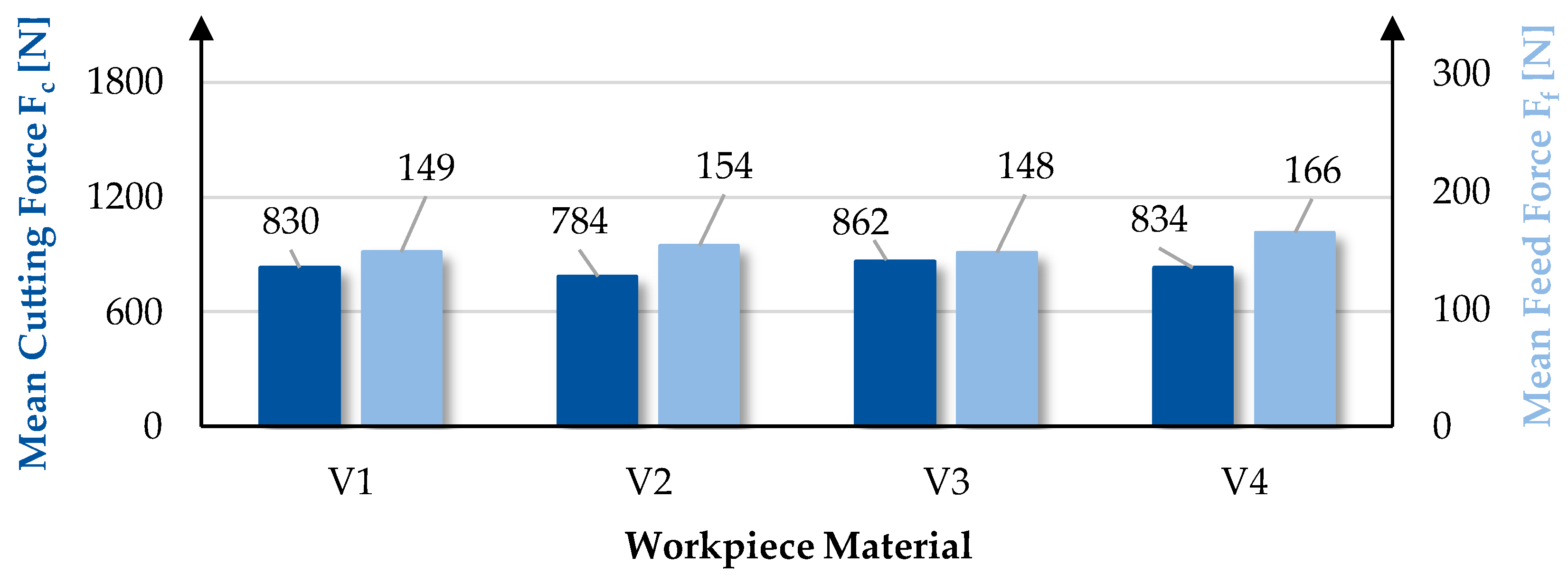
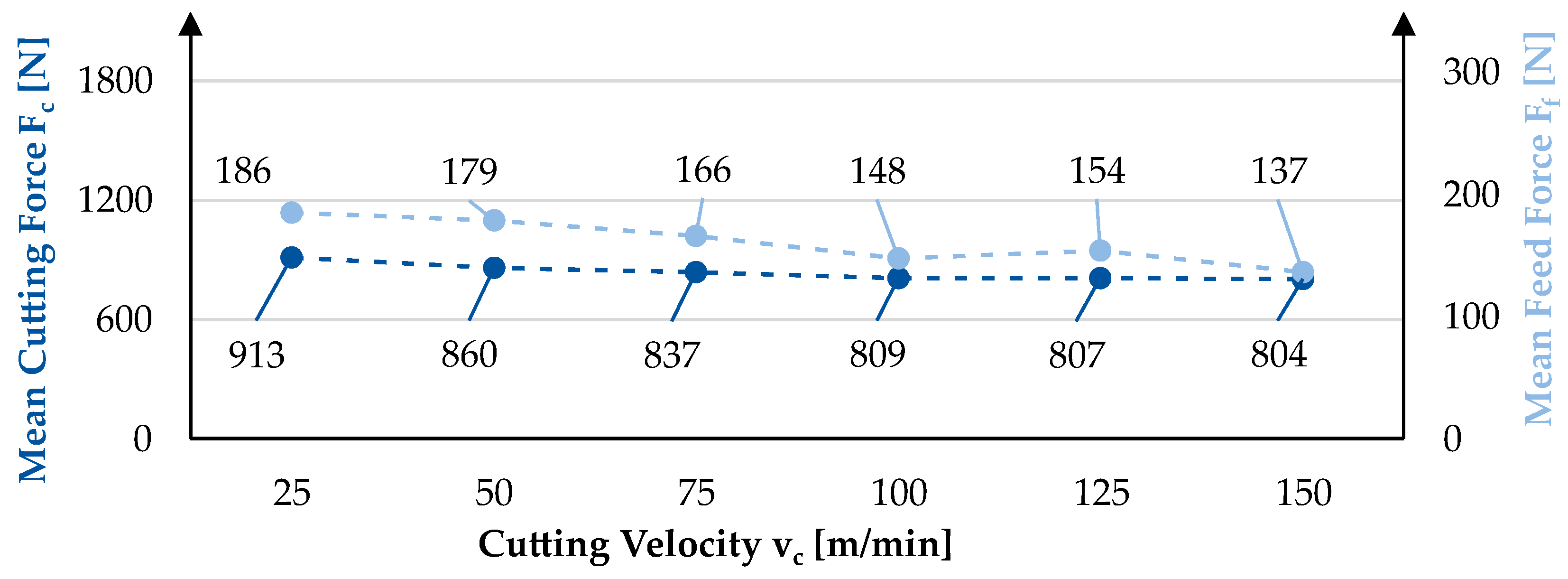
3.1. Cutting Force Components

Increased cutting force components Fi result in higher loads on the tool, the machine, and the workpiece and are, therefore, generally undesirable. To evaluate the influence of the material production route on the cutting force components, these were recorded at all test points using the dynamometer. With engagement conditions of the orthogonal cutting process, the passive force Fp does not exist in theory and is so small in practice that it can be neglected. For this reason, only the cutting force Fc and the feed force Ff were taken into consideration for the evaluation. The main effects of the material-side and process-side variation variables are analyzed and compared below.
Figure 5. Main effect of workpiece material on cutting force components Fi.
Metals 14 00747 g005
As with the measured differences in mechanical properties between all materials, the material production route also had an influence on the cutting force components. While V3 resulted in the highest average cutting force of Fc,V3 = 862 N, V2 resulted in the lowest cutting force of Fc,V2 = 784 N. This means that the material production route influences the level of the cutting force Fc on average by ΔFc,Material = 10%. The material variants V1 and V4 are in between with a cutting force of Fc,V1 = 830 N and Fc,V4 = 834 N and differ only slightly from each other. When considering the feed force in addition to the cutting force, it is noticeable that the feed force Ff behaves in the opposite direction to the cutting force Fc. V4 has the highest feed force with Ff,V2 = 166 N and V3 has the lowest with Ff,V3 = 148 N, whereby the material production route influences the feed force on average by ΔFf,Material = 11.89%. To better understand the opposing behavior of the two cutting force components, the cutting force ratio was also analyzed. The cutting force ratio approximates the coefficient of friction between the chip and rake face of the tool neglecting the plowing effect and the friction between the tool flank face and the workpiece [6,38,39]. V2 and V4 had the highest cutting force ratio ((FT/FN)V2 = 0.375 and (FT/FN)V4 = 0.377), while the cutting force ratio was slightly lower for the variants V1 and V4 ((FT/FN)V1 = 0.356 and (FT/FN)V3 = 0.348). This is consistent with the identified anomaly in the influence of material production route on cutting force Fc and feed force Ff. For the variants V2 and V4 with a higher cutting force ratio, there is in principle a higher proportion of friction between the chip and the rake face, which leads to a redistribution of the force components in which the cutting force is lower and the feed force is higher (Figure 5). Similarly, the lower cutting force ratio in variants V1 and V3 indicates a lower friction between the chip and the rake face and consequently leads to an increase in the cutting force with a simultaneous decrease in the feed force. However, this behavior is not consistent with the determined friction coefficients, where V2 had the lowest friction coefficient and V3 had the highest friction coefficient (Table 2). This is due to two reasons: first, the cutting force ratio neglects the proportion of friction between the flank face and the workpiece that exists in reality, and second, the chip formation processes differ so much between the four material variants that the contact surfaces between the chip and the rake face are very different. In addition to the influence of the material, the influence of the process parameters on the cutting force components was analyzed and presented in the main effect diagrams averaged for all materials (Figure 6 and Figure 7). Due to the large parameter range of feed rate f (0.01 mm ≤ f ≤ 0.5 mm) and cutting velocity vc (25 m/min ≤ vc ≤ 150 m/min), the influence of the feed rate was significantly higher than that of the investigated material properties (ΔFc,Feedrate = +4041%). Due to the continuously increasing chip cross-section, the cutting and feed force increased continuously as the feed rate increased. At a feed rate of f = 0.01 mm, the average cutting force was Fc,f=0.01mm = 41 N and the feed force was Ff,f=0.01mm = 23 N, while at a maximum feed rate of f = 0.5 mm, cutting force components of Fc,f=0.5mm = 1657 N and Ff,f=0.5mm = 285 N were measured (Figure 6).
Figure 6. Main effect of feed rate f on cutting force components Fi.
Metals 14 00747 g006
The variation in the cutting speed had a comparably sized influence, with ΔFc,cutting velocity = −11.9% as the variation of the material production route. An increase in the cutting speed led to a reduction in the two cutting force components on average, which can be attributed to thermal material softening [37,38,40]. At a cutting speed of vc = 25 m/min and an average chip temperature of Tchip = 109 °C, the average cutting force was Fc,vc=25m/min = 913 N and the feed force was Ff,vc=25m/min = 186 N. For the maximum cutting speed of vc = 150 m/min and an average chip temperature of Tchip = 151 °C, cutting force components of Fc,vc=150m/min = 804 N and Ff,vc=150m/min = 137 N were measured (Figure 7).
Figure 7. Main effect of cutting velocity vc on cutting force components Fi.
Metals 14 00747 g007

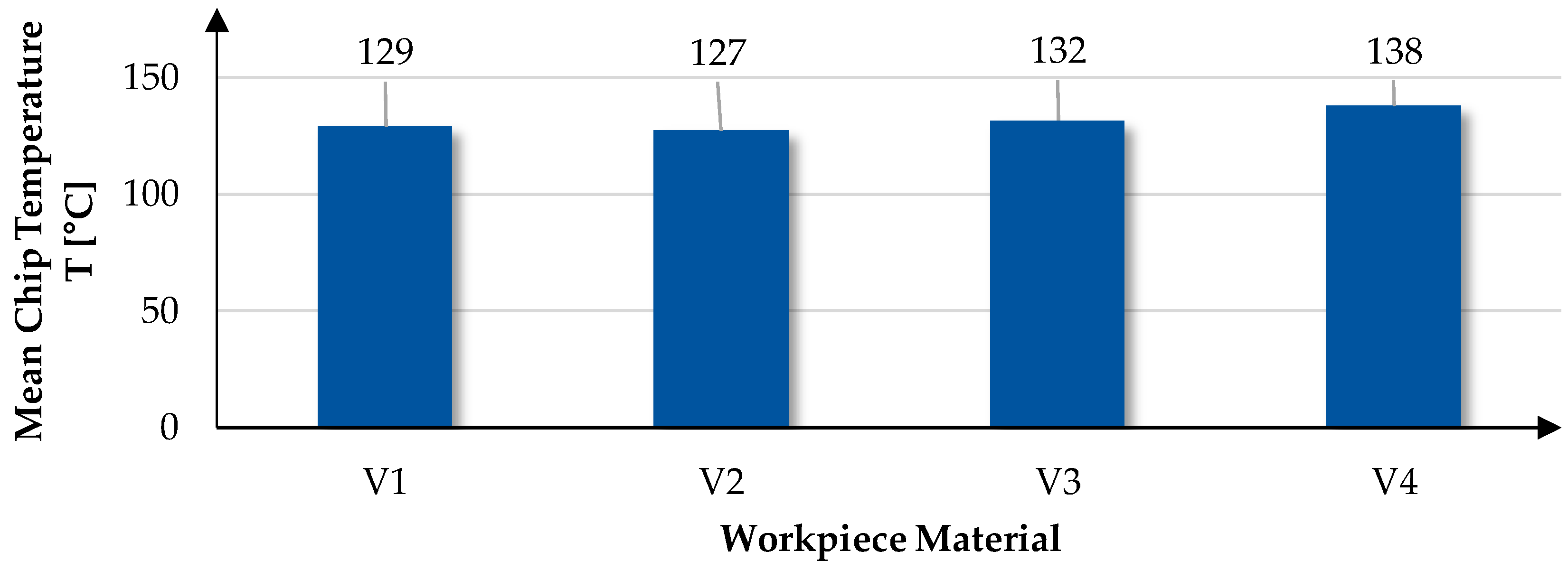
3.2. Cutting Temperature

The selected variations in the material production route showed a low influence on the cutting temperature in the machining tests carried out (Figure 6, Figure 7 and Figure 8). With a chip temperature of TChip,V2 = 127 °C, the lowest average temperature was detected for material variant V2, while variant V4 showed the highest cutting temperature with TChip,V4 = 138 °C. The high work hardening without heat treatment and the lower coefficient of friction in variant V2 ensure less plastic deformation in the primary shear zone. This results in a lower temperature during the process. Both heat-treated variants V3 and V4 showed slightly higher temperatures than the two non-heat-treated variants V1 and V2. This effect can be attributed to the higher coefficient of friction and the resulting increased heat generation (Table 2). It can be concluded that the varied microstructure with coarser grains also ensures a slight increase in temperature and thus leads to a higher thermal softening of the machined material during the process. With a maximum temperature difference of ΔTChip = 7.8% between variants V2 and V4, the influence of the selected work hardening variation and heat treatment can be classified as low. An exemplary thermographic image of the chip temperature and the chip temperature distribution is given in Appendix A (Figure A7).
Figure 8. Main effect of workpiece material on chip temperature.
Metals 14 00747 g008

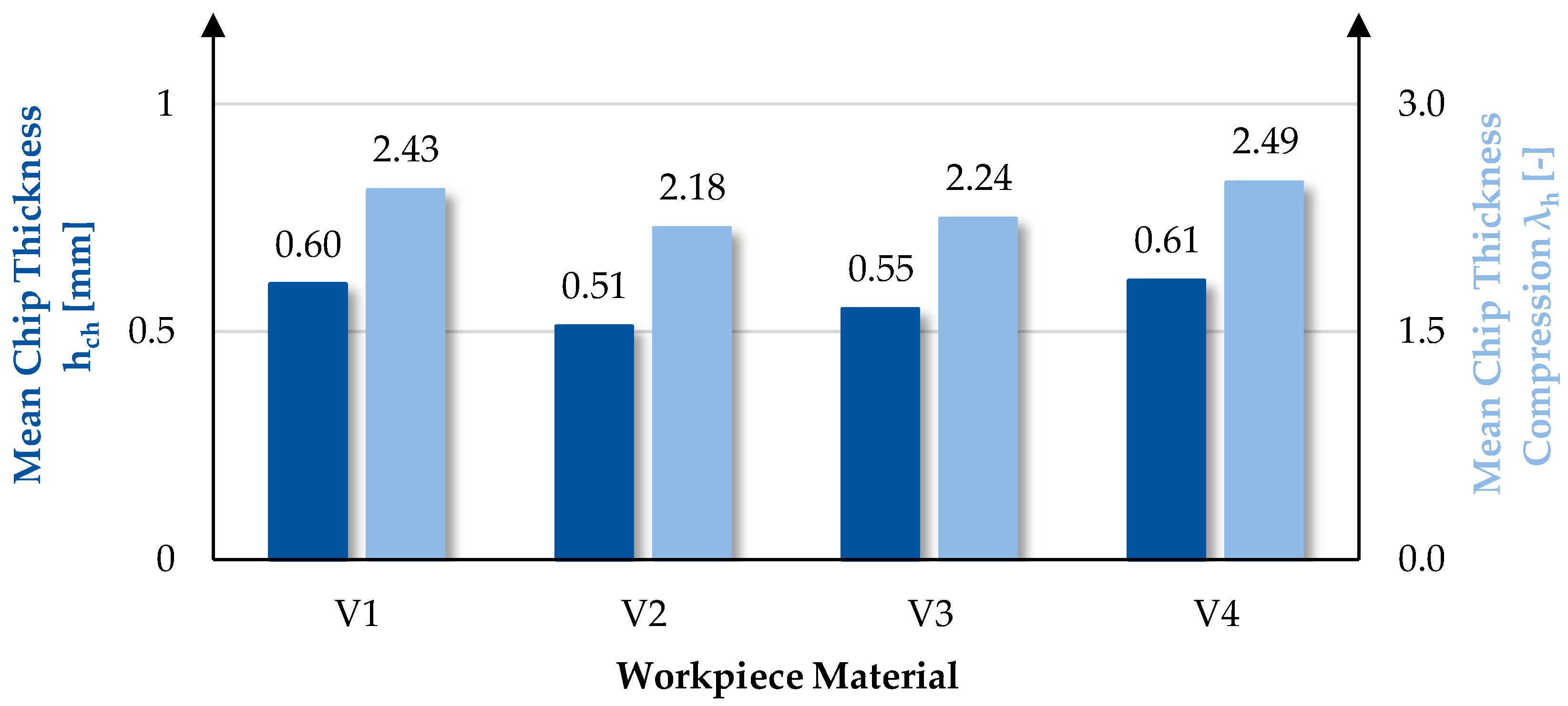
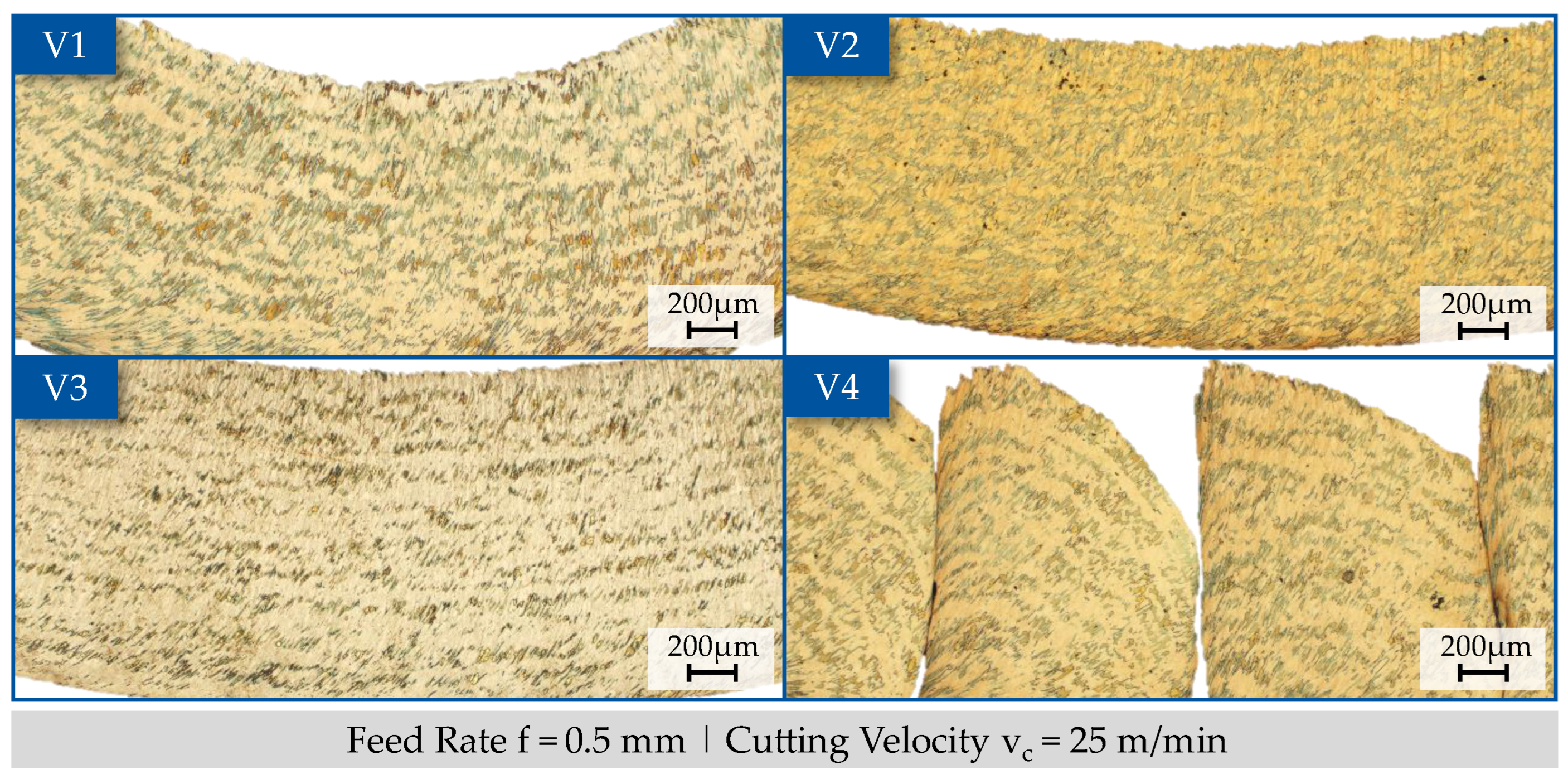
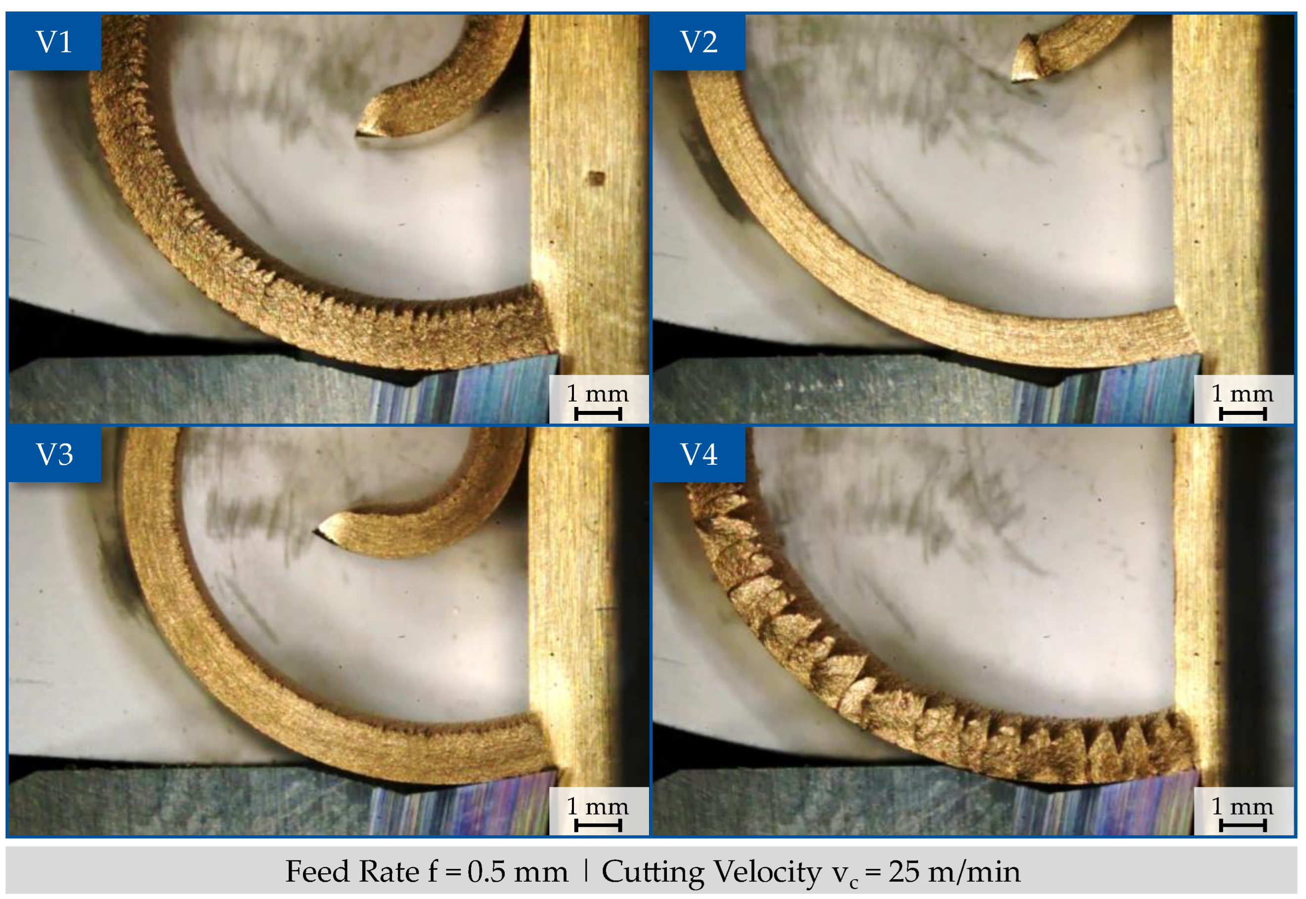
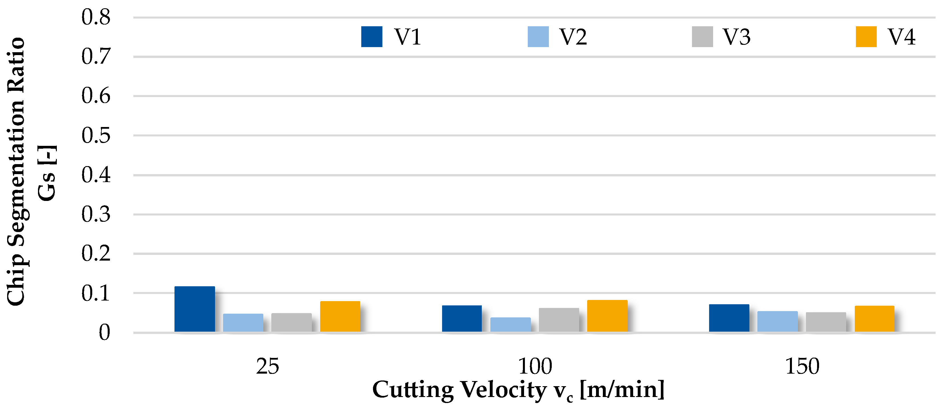
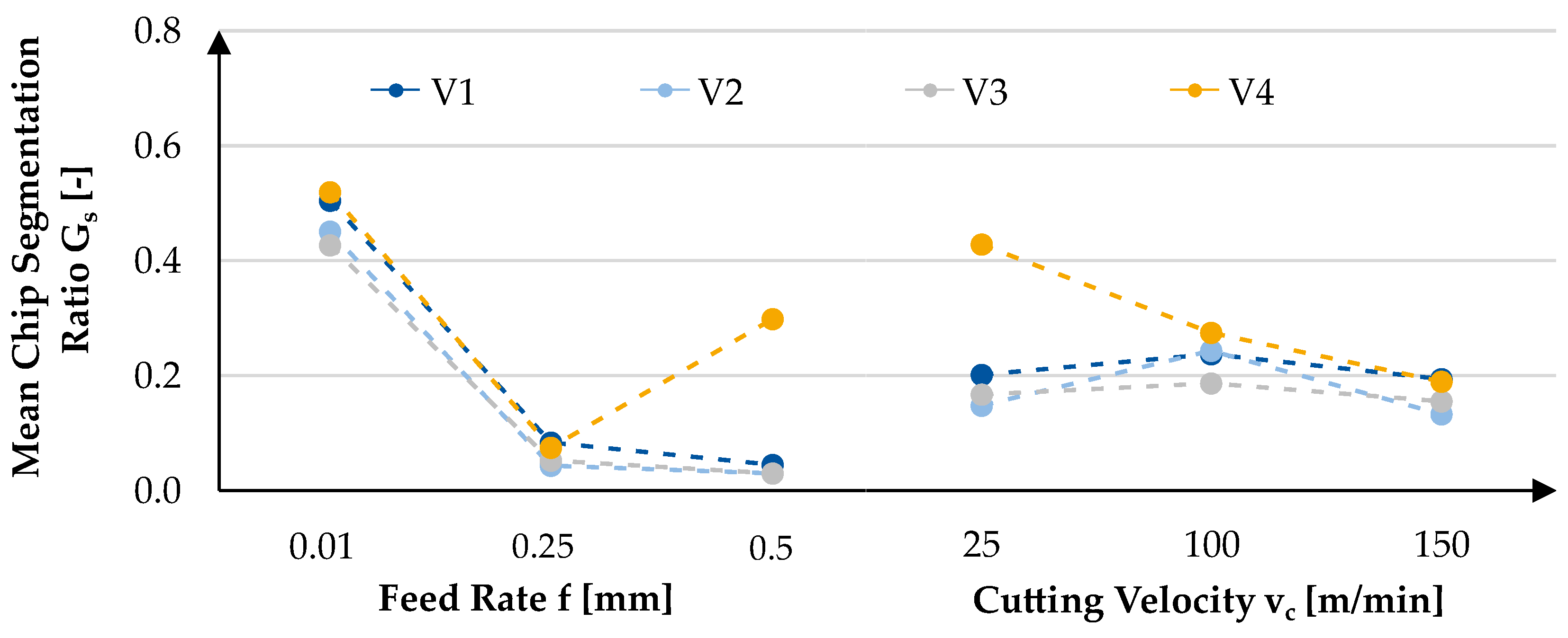
3.3. Chip Formation and Resulting Chip Form

The resulting chip shape is a critical evaluation criterion for the machinability of a material, particularly in the case of lead-free copper-based materials. Lead-free binary CuZn-alloys tend to form long chip shapes (snarled chips and long helical chips), which have a negative impact on the machining process and can jeopardize process reliability in mass production processes. Through a targeted material design, there is the potential to manipulate the underlying chip formation mechanisms in a targeted manner in order to force a favored chip breakage and thus realize process-safe machining of lead-free binary CuZn-alloys. In order to understand the underlying mechanisms of chip formation and how these are influenced by the mechanical and microstructural properties of the workpiece material, a detailed evaluation of the resulting chip morphology and the chip formation process was carried out. Therefore, the resulting chips were photographed and measured using a digital light microscope type Keyence VHX-900F (Keyence, Osaka, Japan). The evaluation variables chip thickness h’, chip thickness ratio λh, chip curvature radius ru, and degree of chip segmentation GS were derived from these measurements for analyzing the chip shape. In addition, the chip formation mechanisms were analyzed by a qualitative evaluation of high-speed videos of the chip formation process and longitudinal etched chip sections.
The variation in the material manufacturing route had a higher influence on chip formation than on the cutting force components and the chip temperature. This is evident when analyzing the chip morphology (Figure A6). The average chip thickness and chip thickness compression ratio λh were highest for material V4 with λh,V4 = 2.49, followed by variant V1 with λh,V1 = 2.43 (Figure 9). The two variants V3 and V2 have shown a significantly lower chip thickness compression ratio λh on average with λh,V3 = 2.24 and λh,V2 = 2.18, respectively. This results in a maximum difference in chip thickness compression ratio of 14.2% between V4 and V2. In addition to the main effect diagram (Figure 9), the material influences were analyzed for individual parameters (Figure A1 and Figure A2) to check validity. Here, it was found that the material influence at a feed rate of f = 0.25 mm was qualitatively the same as in the main effect diagram, regardless of the choice of cutting speed vc. At low feed rates (f = 0.01 mm), the non-heat-treated variants V1 and V2 showed slightly higher chip thickness compression ratio than the non-heat-treated variants, while at high feed rates (f = 0.5 mm), only V1 showed a significantly higher chip thickness compression ratio. It can, thus, be summarized that, on average, a lower work hardening and the heat treatment applied lead to a higher chip thickness compression ratio, but the underlying mechanisms of action are feed rate-dependent, and a different behavior can be observed at very small or very large feed rates.
Figure 9. Main effect of workpiece material on chip thickness and chip thickness compression ratio.
Metals 14 00747 g009
The degree of chip segmentation Gs was qualitatively influenced by the material like the chip thickness hch and chip thickness compression ratio λh. Material variant V4 had the highest degree of chip segmentation with Gs,V4 = 0.30. Variant V1 followed with Gs,V1 = 0.21, while V2 and V3 had lower average degrees of chip segmentation with Gs,V2 = 0.18 and Gs,V3 = 0.17, respectively. It can be summarized that increased work hardening resulted in a slight reduction in chip segmentation. Furthermore, the heat treatment caused an increase in the degree of chip segmentation Gs. Similar to the analysis of the chip thickness compression ratio, the material influences were also analyzed for individual parameters (Figure A3 and Figure A4). It was found that the influence of feed rates of f ≥ 0.25 mm is represented very well in the main effect diagram (Figure 10) and that the less strain-hardened variants V1 and V4 tended to exhibit higher chip segmentation. At lower feed rates (f = 0.01 mm), the chip segmentation was significantly higher and the influence of the material was different (Figure A3). Here, V2 (Gs,V2,f=0.01mm = 0.60) and V4 (Gs,V4,f=0.01mm = 0.68) showed the highest degree of chip segmentation, while V3 showed a much lower degree of chip segmentation (Gs,V3,f=0.01mm = 0.45). This very different behavior at low feed rates is due to the microstructure. At a feed rate of f = 0.01 mm, the chips had a chip thickness between 20.6 µm ≤ hch ≤ 28.91 µm. The chip thickness was thus in the range of the grain diameters of the individual phases (Table 3). When analyzing the corresponding longitudinal chip sections, it can be seen that the grains of the ß-phase extend over the entire thickness of the chip and that there is a much stronger chip segmentation in the areas with ß-phase (Figure A5). From this, it can be concluded that at small feed rates, the chip segmentation behavior is primarily determined by the distribution of the ß-phase. Larger connected ß-phase areas, which increasingly extend over the entire chip thickness as in V1, V2 and V4, can thus favor increased chip segmentation. The influence of the material on the chip curvature radius ru was qualitatively different compared to the other evaluation variables. Among the material variants tested, V1 achieved the highest average chip curvature radius with ru,V1 = 1.32 mm, followed closely by V2 with ru,V2 = 1.26 mm and V4 with ru,V4 = 1.23 mm. The work hardening in variants V2 and V3 resulted in a slightly lower chip curvature radius, while the influence of heat treatment (V3 and V4) was much more significant. Both heat-treated materials showed a significantly lower radius of curvature than the two identically work-hardened but non-heat-treated variants V1 and V4. This can be explained by the mechanical properties, especially the strength, of the materials. For example, the heat treatment of V3 resulted in a significantly lower tensile strength compared to variant V2 (Table 2). As a consequence, the resistance to plastic deformation decreased, leading to a lower resistance to natural chip curvature. This ultimately resulted in the smallest chip curvature radius ru. The less work-hardened variants V1 and V4 exhibited a similar trend. However, due to the sequence of process steps in the semi-finished product production route (first annealing and then drawing), variant V4 had only a slightly lower chip curvature radius than V1. This trend corresponds to that of the strength parameters (Table 2). Overall, the differences in chip curvature radius were smaller than those for the degree of chip segmentation Gs and the chip thickness h or the chip thickness compression ratio λh.
Figure 10. Main effect of workpiece material on chip segmentation and chip curvature radius.
Metals 14 00747 g010
In addition to the shown and discussed influences, some further interactions between the process parameters and the material variants were detected when analyzing the influence of the material on the chip shape. For variants V1–V3, the degree of chip segmentation Gs decreased strictly monotonically as the feed rate increased. Variant V4 exhibited different behavior compared to variants 1-3 at high feed rates (Figure 11). Above the central feed rate of f = 0.25 mm, the chip segmentation Gs increased significantly once again. Additional results can be obtained by considering the interactions between the cutting speed vc and the degree of chip segmentation Gs (Figure 11). For material variants V1–V3, the influence of cutting speed on chip segmentation is negligible. However, variant V4 exhibits significantly stronger segmentation at low cutting speeds. At the lowest cutting speed of vc = 25 m/min, the degree of chip segmentation was measured to be Gs = 0.43. At the maximum cutting speed of vc = 150 m/min, the degree of chip segmentation was measured to be only Gs = 0.19 (Figure 11). The deviating chip formation behavior of V4 at high feed rates and low cutting speeds was also confirmed by the individual analysis of each test point. The behavior was particularly pronounced for one test point. At a high feed rate of f = 0.5 mm and a low cutting speed of vc = 150 m/min, the chip formation of material variant V4 behaved completely differently to the other materials and to the other process parameter combinations analyzed. Increased segmentation of the chip and formation of adiabatic shear bands could be recognized, which was not the case for any of the other parameter points investigated. This phenomenon was analyzed in more detail in order to identify the underlying mechanisms of action by means of a qualitative analysis of the high-speed images as well as the longitudinal chip sections (Figure 12 and Figure 13).
When analyzing the chip formation video, it is visible that the chip of V4 for a feed rate of f = 0.5 mm and a cutting velocity of vc = 25 m/min does not run continuously over the rake face of the tool, as is the case with the other material variants. The chip is formed according to a cyclically repeating pattern and flows discontinuously across the rake face. Initially, the material in the form of the chip does not flow over the rake face but is compressed to a certain extent. As soon as a certain degree of compression is reached, the material begins to flow in the form of a chip over the rake face before the flow of the chip slows down again and the material builds up again on the rake face up to a specific degree of compression. This process is repeated cyclically every t = 4.47 ms. The described acyclic chip formation results in a highly segmented chip that is about to break (Figure 13). The longitudinal chip sections recorded (Figure 12) confirm the significantly stronger chip segmentation of material variant V4 compared to variants V1–V3. The degree of chip segmentation at this parameter setting for variant V4 is Gs = 0.791, while the other materials have a typical continuous chip with 0.031 ≤ Gs ≤ 0.041. In addition, the etched longitudinal microsections of the chips showed clear differences between the material variants in the arrangement, distribution, and morphology of the various phases for different process parameters. Particularly noticeable was a strong shearing of the β-phase in the cross-chip direction in material variant V4, which extended over the entire chip thickness. This shear was also present in the three other variants but was much less pronounced. The highly work-hardened variants V2 and V3 in particular exhibited significantly weaker deformation of the β-phase, which only extended over about half the chip thickness. This different shear behavior is possibly due to differences in the distribution of the β-phase. When analyzing the EBSD phase map of the four material variants, it was noticed that the β-phase in material variant V4 is much more finely distributed than in the other material variants. This finer distribution, which was introduced into the material by the heat treatment followed by a slight work hardening, visibly leads to greater shear over the entire chip thickness. This also results in the formation of adiabatic shear bands over the entire chip, which could ultimately be responsible for the strong segmentation during the process with the parameter combination of high feed rate and low cutting speed. This hypothesis is confirmed once again by the longitudinal microsections (Figure 12). The longitudinal section of the chip of material variant V4 shows varying degrees of deformation of the phases in different areas of the chip. While almost no deformation of the phases can be recognized in the interior of the individual chip segments, the deformation is concentrated near the shear at the edge of the individual chip segments.
Figure 12. Longitudinal microsections of the chips.
Metals 14 00747 g012
Figure 13. Influence of the workpiece material on chip formation.
Metals 14 00747 g013

4. Conclusions

The aim of this study was to analyze the impact of a variation in the material production route of CuZn40 (CW509L) on the material properties, especially on machinability. It was observed that the variation in the degree of work hardening and heat treatment influences the machinability properties of the material and can have a significant influence on the underlying chip formation mechanisms and the resulting chip shape, particularly during interaction with the selected process parameters. The key findings of this study can be summarized as follows:
The different material properties, which were introduced by varying the material production route, resulted in changes in the cutting force components. The change in cutting force between the materials investigated was ΔFc,material = 10%, and the change in feed force was ΔFf,material = 11.89%. In particular, a higher coefficient of friction as a result of heat treatment led to an increase in the cutting force.
The variation in the material production route had a small influence of ΔTChip,material = 7.8% on the chip temperature. The reduced coefficient of friction and increased strength resulting from high work hardening and the absence of heat treatment resulted in low chip temperatures TChip in the machining process due to reduced deformations in the primary shear zone.
The adjustment of the material production route had the highest effect on the underlying chip formation mechanisms and the resulting chip shape.
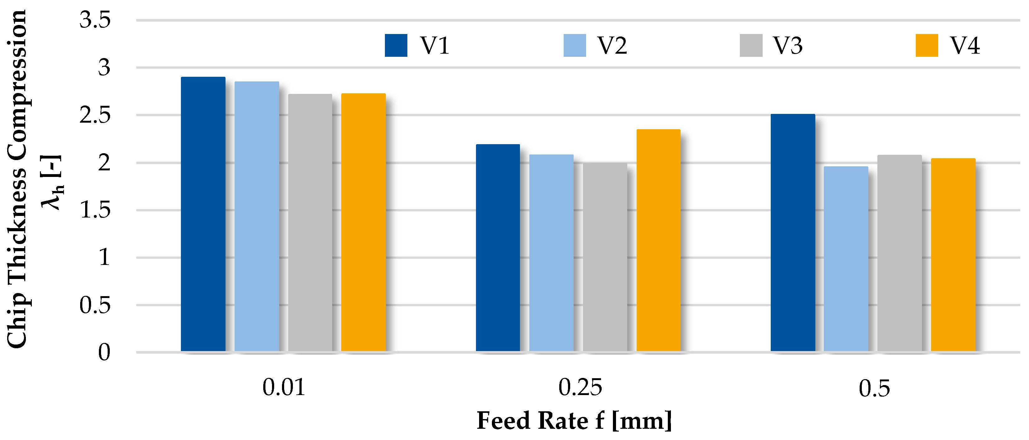
On average, a lower work hardening and the use of a heat treatment lead to a higher chip thickness compression ratio, but the underlying mechanisms of action are feed rate-dependent and a different behavior can be observed at very small or very high feed rates.
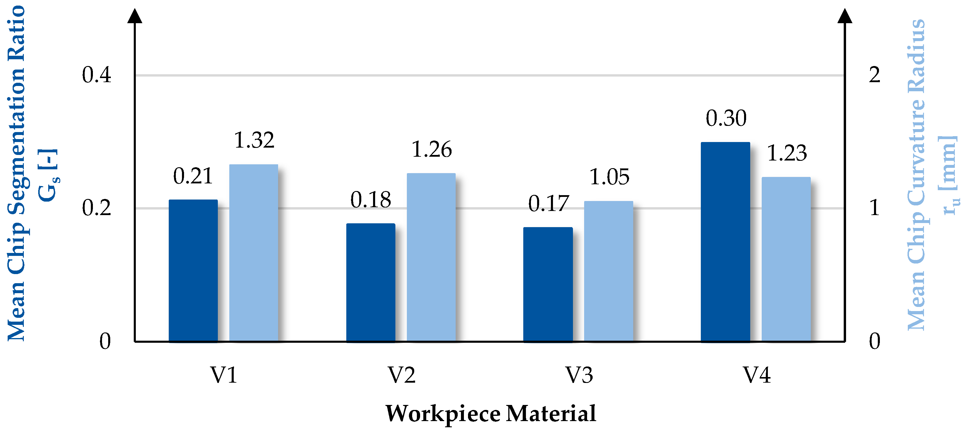
In general, the chip segmentation Gs increased with a decrease in work hardening. Furthermore, the heat treatment caused an increase in the degree of chip segmentation. Nevertheless, process parameter-dependent changes in the chip formation mechanism led to different behavior when using small feed rates of f = 0.01 mm.
At lower feed rates (f = 0.01 mm) a size effect was recognized: the chip segmentation was significantly higher and the influence of the material production route was different in comparison to the other process parameter settings. Due to the low chip thickness of 20.6 µm ≤ hch ≤ 28.91 µm, there were areas in the chip where the ß-phase extended over the entire chip thickness. This resulted in significantly increased segmentation in these areas. For small chip thicknesses, the distribution and size of the ß-phase areas are therefore particularly relevant for the chip formation mechanisms and the resulting chip segmentation. Due to a larger proportion of ß-phase in the microstructure, this behavior was more pronounced in material variant V2.
For the material variant V4, which was heat-treated before work hardening, strong differences in chip formation were identified for high feed rates of f = 0.5 mm and low cutting speeds of vc = 25 m/min, which suggests an interaction between material properties and process parameters, as this phenomenon only occurs with V4. With the material-process parameter combination described, a discontinuous chip formation process occurs, resulting in a highly segmented chip. The cause is assumed to be the finer distribution of the ß-phase at V4, which causes the acyclic sliding of the chip over the rake face under the given boundary conditions. To investigate this hypothesis, the chip formation of the material should be analyzed under similar boundary conditions in chip root investigations.
In this study, precious new knowledge on the influence of the semi-finished product production route on the machinability of lead-free copper-zinc alloys was obtained. Particularly with regard to the analysis of the chip formation mechanisms, the hypotheses put forward must be validated by further investigations, and the underlying mechanisms of action must be better understood. To this end, the authors have already planned further investigations with the same materials in advanced machining tests and the preparation of chip root tests. In addition, to validate the influence of the semi-finished product production route on machinability, further brass materials with an even more extensive variation of the semi-finished product production route are to be analyzed with regard to their machinability.

Author Contributions

Conceptualization, K.B.; methodology, K.B.; software, K.B.; validation, K.B., S.K. and M.M.; formal analysis, K.B. and M.M.; investigation, K.B. and S.K.; resources, K.B., M.M. and T.B.; data curation, K.B. and S.K.; writing—original draft preparation, K.B. and M.M.; writing—review and editing, K.B., M.M. and T.B.; visualization, K.B. and S.K.; supervision, K.B., M.M. and T.B.; project administration, K.B.; funding acquisition, K.B. and T.B. All authors have read and agreed to the published version of the manuscript.

Funding

This work was funded in part by the Innovation Network Copper Processing (IKB).

Data Availability Statement

The raw data supporting the conclusions of this article will be made available by the authors on request.

Acknowledgments

The authors would like to thank the members of the Innovation Network Copper Processing (IKB) for supporting this study, for providing materials, and for sharing cross-industry know-how in close cooperation within the project.

Conflicts of Interest

The authors declare no conflicts of interest.

Appendix A

Figure A1. Influence of the workpiece material on chip thickness ratio for different feed rates f.
Metals 14 00747 g0a1
Figure A2. Influence of the workpiece material on chip thickness ratio for different cutting velocities vc.
Metals 14 00747 g0a2
Figure A3. Influence of the workpiece material on chip segmentation ratio for different feed rates f.
Metals 14 00747 g0a3
Figure A4. Influence of the workpiece material on chip segmentation ratio for different cutting velocities vc.
Metals 14 00747 g0a4
Figure A5. Chip segmentation for small feed rates depending on the β-phase distribution.
Metals 14 00747 g0a5
Figure A6. Evaluation of chip morphology using high-speed videos and longitudinally etched chip sections.
Metals 14 00747 g0a6
Figure A7. Thermographic recording of chip temperature and chip temperature distribution.
Metals 14 00747 g0a7

References

  1. Johansson, J.; Alm, P.; M’Saoubi, R.; Malmberg, P.; Stahl, J.-E.; Bushlya, V. On the function of lead (Pb) in machining brass alloys. Int. J. Adv. Manuf. Technol. 2022, 120, 7263–7275. [Google Scholar] [CrossRef]
  2. Nobel, C.; Klocke, F.; Lung, D.; Wolf, S. Machinability Enhancement of Lead-free Brass Alloys. Procedia CIRP 2014, 14, 95–100. [Google Scholar] [CrossRef]
  3. Schultheiss, F. Machinability of CuZn21Si3P brass. Mater. Sci. Technol. 2016, 32, 1744–1750. [Google Scholar] [CrossRef]
  4. Zachert, C.; Brans, K.; Schraknepper, D.; Bergs, T. Assessment and Comparison of the Machinability of Innovative Copper Alloys. In Proceedings of the Copper Alloys 2022, Düsseldorf, Germany, 22–23 November 2022; Volume 1, pp. 56–59. [Google Scholar]
  5. Müller, M.S. Machinability of Low-Lead and Lead-Free Brass Alloys. Ph.D. Dissertation, NTNU, Trondheim, Norway, 2024. [Google Scholar]
  6. Nobel, C.; Klocke, F.; Veselovac, D. Influence of tool material and coating on the machinability of low-leaded brass alloys in turning. Mater. Manuf. Process. 2016, 31, 1895–1903. [Google Scholar] [CrossRef]
  7. Müller, M.S.; Brans, K.; Meurer, M.; Sørby, K.; Bergs, T. The effect of high-pressure cutting fluid supply on the chip breakability of lead-free brass alloys. Int. J. Adv. Manuf. Technol. 2023, 129, 4317–4333. [Google Scholar] [CrossRef]
  8. Müller, M.S.; Sørby, K. The Influence of the Rake Angle on the Cutting of Low-Lead and Lead-Free Brass Alloys. In Manufacturing Driving Circular Economy; Kohl, H., Seliger, G., Dietrich, F., Eds.; Springer International Publishing: Cham, Switzerland, 2023; pp. 219–227. ISBN 978-3-031-28838-8. [Google Scholar]
  9. Laakso, S.V.A.; Hokka, M.; Niemi, E.; Kuokkala, V.-T. Investigation of the effect of different cutting parameters on chip formation of low-lead brass with experiments and simulations. Proc. Inst. Mech. Eng. Part B J. Eng. Manuf. 2013, 227, 1620–1634. [Google Scholar] [CrossRef]
  10. Nobel, C.; Hofmann, U.; Klocke, F.; Veselovac, D. Experimental investigation of chip formation, flow, and breakage 5 in free orthogonal cutting of copper-zinc alloys. Int. J. Adv. Manuf. Technol. 2015, 84, 1127–1140. [Google Scholar] [CrossRef]
  11. Stavroulakis, P.; Toulfatzis, A.I.; Pantazopoulos, G.A.; Paipetis, A.S. Machinable Leaded and Eco-Friendly Brass Alloys for High Performance Manufacturing Processes: A Critical Review. Metals 2022, 12, 246. [Google Scholar] [CrossRef]
  12. Brans, K.; Baier, S.; Schraknepper, D.; Bergs, T. Empirical Studies on the Influence of Tool and Process Parameters on the Machinability in Plunge Milling of Lead-Free CuZn-Alloys. Procedia CIRP 2022, 115, 113–118. [Google Scholar] [CrossRef]
  13. Baier, S. Tool Geometry Analysis for Plunge Milling of Lead-Free CuZn-Alloys. In Proceedings of the 24th International Conference on Material Forming, Online, 14–16 April 2021. [Google Scholar]
  14. Baier, S.; Brans, K.; Schraknepper, D.; Bergs, T. Experimental optimization of tool geometry and lubricoolant supply in plunge milling of lead-free Brass. In Proceedings of the Copper Alloys 2022, Düsseldorf, Germany, 22–23 November 2022; Volume 1, pp. 4–7. [Google Scholar]
  15. Twarog, D.L. Modified Red Brass With Bismuth and Selenium: Research Result. AFS Trans. 1995, 103, 451–461. [Google Scholar]
  16. Imai, H.; Shufeng, L.; Atsumi, H.; Kosaka, Y.; Kojima, A.; Kondoh, K. Development of Lead-Free Machinable Brass with Bismuth and Graphite Particles by Powder Metallurgy Process. Mater. Trans. 2010, 51, 855–859. [Google Scholar] [CrossRef]
  17. Saigal, A. Machinability of Cast Lead-Free Yellow Brass Containing Graphite Particles. AFS Trans. 1996, 104, 225–228. [Google Scholar]
  18. Imai, H. Characteristics of Lead-Free P/M Cu60-Zn40 Brass Alloys with Graphite. Trans. JWRI 2008, 37, 51–55. [Google Scholar]
  19. Taha, M.A.; El-Mahallawy, N.A.; Hammouda, R.M.; Moussa, T.M.; Gheith, M.H. Machinability characteristics of lead free-silicon brass alloys as correlated with microstructure and mechanical properties. Ain Shams Eng. J. 2012, 3, 383–392. [Google Scholar] [CrossRef]
  20. Yang, C. High-strength and free-cutting silicon brasses designed via the zinc equivalent rule. Mater. Sci. Eng. A 2018, 723, 296–305. [Google Scholar] [CrossRef]
  21. Schultheiss, F.; Johansson, D.; Bushlya, V.; Zhou, J.; Nilsson, K.; Ståhl, J.-E. Comparative study on the machinability of lead-free brass. J. Clean. Prod. 2017, 149, 366–377. [Google Scholar] [CrossRef]
  22. Toulfatzis, A.; Pantazopoulos, G.; David, C.; Sagris, D.; Paipetis, A. Final Heat Treatment as a Possible Solution for the Improvement of Machinability of Pb-Free Brass Alloys. Metals 2018, 8, 575. [Google Scholar] [CrossRef]
  23. Toulfatzis, A.I.; Pantazopoulos, G.A.; Paipetis, A.S. Microstructure and properties of lead-free brasses using post-processing heat treatment. Mater. Sci. Technol. 2016, 32, 1771–1781. [Google Scholar] [CrossRef]
  24. Toulfatzis, A.I.; Besseris, G.J.; Pantazopoulos, G.A.; Stergiou, C. Characterization and comparative machinability investigation of extruded and drawn copper alloys using non-parametric multi-response optimization and orthogonal arrays. Int. J. Adv. Manuf. Technol. 2011, 57, 811–826. [Google Scholar] [CrossRef]
  25. Vilarinho, C. Influence of the chemical composition on the machinability of brasses. J. Mater. Process. Technol. 2005, 170, 441–447. [Google Scholar] [CrossRef]
  26. Vazdirvanidis, A.; Rikos, A.; Toulfatzis, A.I.; Pantazopoulos, G.A. Electron Backscatter Diffraction (EBSD) Analysis of Machinable Lead-Free Brass Alloys: Connecting Texture with Fracture. Metals 2022, 12, 569. [Google Scholar] [CrossRef]
  27. Stavroulakis, P.; Toulfatzis, A.I.; Pantazopoulos, G.; Paipetis, A.S. A Review of Industrial Brass Alloys towards High Productivity Machining Processes. In Proceedings of the 8th International Conference of the Hellenic Metallurgical Society, Patras, Greece, 14–16 December 2022. [Google Scholar]
  28. Hofmann, U. Über den Einfluss von Werkstoffkennwerten auf das Spanbruchverhalten von bleiarmem Messing. Materialwiss. Werkstofftech. 2018, 49, 753–768. [Google Scholar] [CrossRef]
  29. Chaskis, S.; Maritsa, S.; Stavroulakis, P.; Papadopoulou, S.; Goodall, R.; Papaefthymiou, S. Compositional Design and Thermal Processing of a Novel Lead-free Cu–Zn–Al–Sn Medium Entropy Brass Alloy. Metals 2024, 14, 620. [Google Scholar] [CrossRef]
  30. DIN Deutsches Institut für Normung e.V. Zugversuch: Teil 1: Prüfvwerfahren bei Raumtemperatur; Beuth Verlag GmbH: Berlin, Germany, 2020; 77.040.10 (6892-1). [Google Scholar]
  31. DIN Deutsches Institut für Normung e.V. Prüfung Metallischer Werkstoffe–Druckversuch bei Raumtemperatur; Beuth Verlag GmbH: Berlin, Germany, 2023; 77.040.10 (50106). [Google Scholar]
  32. ISO 6507-1:2023; Metallic Materials—Vickers Hardness Test-Part 1: Test Method. ISO: Geneva, Switzerland, 2023.
  33. ISO 14577-1; Metallic Materials-Instrumented Indentation Test for Hardness and Materials Parameters-Part 1: Test Method. ISO: Geneva, Switzerland, 2015.
  34. DIN Deutsches Institut für Normung e.V. Metallische Werkstoffe-Kerbschlagbiegeversuch nach Charpy: Teil 1: Prüfverfahren; Beuth Verlag GmbH: Berlin, Germany, 2017; 77.040.10 (148-1). [Google Scholar]
  35. Puls, H.; Klocke, F.; Lung, D. Experimental investigation on friction under metal cutting conditions. Wear 2014, 310, 63–71. [Google Scholar] [CrossRef]
  36. Puls, H. Mehrskalenmodellierung Thermo-Elastischer Werkstückdeformationen beim Trockendrehen. Ph.D. Dissertation, Rheinisch-Westfälischen Technischen Hochschule Aachen, Aachen, Germany, 2015. [Google Scholar]
  37. Nobel, C. Application of a new, severe-condition friction test method to understand the machining characteristics of Cu–Zn alloys using coated cutting tools. Wear 2015, 344, 58–68. [Google Scholar] [CrossRef]
  38. Nobel, C. Drehbearbeitung von Bleiarmen Kupfer-Zink-Legierungen. Ph.D. Dissertation, Rheinisch-Westfälische Technische Hochschule Aachen, Aachen, Germany, 2016. [Google Scholar]
  39. Albrecht, P. New Developments in the Theory of the Metal-Cutting Process: Part I. The Ploughing Process in Metal Cutting. J. Eng. Ind. 1960, 82, 348–357. [Google Scholar] [CrossRef]
  40. Laakso, S.V.A.; Niemi, E. Modified Johnson–Cook flow stress model with thermal softening damping for finite element modeling of cutting. Proc. Inst. Mech. Eng. Part B J. Eng. Manuf. 2015, 230, 241–253. [Google Scholar] [CrossRef]
Figure 1. Overview of the variation in the material production routes.
Metals 14 00747 g001
Figure 2. Light microscopic cross-sections of the material variants V1–V4.
Metals 14 00747 g002
Figure 3. EBSD analysis of the material variants V1–V4.
Metals 14 00747 g003
Figure 4. Experimental setup, cutting conditions, and measurement devices.
Metals 14 00747 g004
Figure 11. Interactions between workpiece material and process parameters regarding chip segmentation.
Metals 14 00747 g011
Table 1. Chemical composition of the test alloy CuZn40 (CW509L).
CuZnFeSnSiPbNiZrPAgSOther
66.61038.9570.1590.1400.1010.0240.0030.0020.0020.0010.0010.001
All values in mass percent mi [%].
Table 2. Mechanical material properties of the material variants V1–V4.
Mechanical Material PropertyV1V2V3V4
Tensile Strength 1—Rm [MPa] 455.5617432.5447
Yield Strength 1—Rp0.2 [MPa]323585200.5315
Elongation at Break 1—A [%]32.0513.1546.0533.2
Compressive Strength 2—Rdb[MPa]1197.512491160.51134.5
Macro-hardness (rim-zone) 3—[HV]145185105140
Macro-hardness (core) 3—[HV]118180103117
Micro-hardness (α-Phase) 4—[HVe]148217163169
Micro-hardness (β-Phase) 4—[HVe]196258208231
Notched Impact Strength 5—ak [J/cm2]12.6 *814.49 *
Friction coefficient at vrel = 50 m/min 6—µ [-]0.420.280.500.41
Friction coefficient at vrel = 75 m/min 6—µ [-]0.390.250.440.38
Friction coefficient at vrel = 100 m/min 6—µ [-]0.350.230.400.35
Friction coefficient at vrel = 125 m/min 6—µ [-]0.320.230.380.33
Friction coefficient at vrel = 150 m/min 6—µ [-]0.300.210.360.29
1 Tensile test according to DIN EN ISO 6892-1 [30]. 2 Compression test according to DIN50106 [31]. 3 Vickers hardness test according to DIN EN ISO 6507-1 [32]. 4 Vickers microhardness test according to DIN EN ISO 14577-1 [33]. 5 Impact test according to DIN EN ISO 148-1 [34]. 6 Friction test under machining conditions according to PULS [35]. * No breakage occurred during the notched bar impact test.
Table 3. Numerical parameters of the microstructural properties of the material variants V1–V4.
Microstructural Material PropertyV1V2V3V4
α-Phase Fraction—φα [%] 81728882
β-Phase Fraction—φβ [%]19281218
Average Grain Area (α-Phase)—ak,α [μm2]337.6143.6123.4228.3
Average Grain Area (β-Phase)—ak,β [μm2]255.4143119.5176.6
Average Grain Diameter (α-Phase)—dα [μm]18.212.81115.7
Average Grain Diameter (β-Phase)—dβ [μm]1612.610.714.1
Grain aspect ratio (α-Phase)—b/h [-]1.92.61.82
Grain aspect ratio (β-Phase)—b/h [-]2.72.72.42.6
Table 4. Experimental design of the machining investigations.
1
Feed
Variation
2
Cutting Speed
Variation
3
Min. and Max.
Variation
Process Orthogonal Cutting
MachineBroaching Machine Type Forst RASX 8 × 2200 × 600 M/CNC
Tool HolderKennametal NSL2525M3
ToolKennametal N3BL (adjusted)
Cutting Tool MaterialCarbide K313
Face Rake Angle γ [°]10
Face Flank Angle α [°]10
Cutting Edge Angle κr [°]90
Cutting Edge Radius rβ [µm]2 µm < rβ < 8 µm
Feed Rate f/mm0.01; 0.05; 0.1; 0.15; 0.2; 0.25; 0.3; 0.35; 0.4; 0.45; 0.50.250.01; 0.5
Cutting Velocity vc [m/min] 10025; 50; 75; 100; 125; 15025; 150
Workpiece MaterialCuZn40 V1, CuZn40 V2, CuZn40 V3, CuZn40 V4
Cooling LubricantDry
Disclaimer/Publisher’s Note: The statements, opinions and data contained in all publications are solely those of the individual author(s) and contributor(s) and not of MDPI and/or the editor(s). MDPI and/or the editor(s) disclaim responsibility for any injury to people or property resulting from any ideas, methods, instructions or products referred to in the content.

