Design of the Input and Output Filter for a Matrix Converter Using Evolutionary Techniques

 ,
,  , ,
, ,  , , and
Abstract
:
1. Introduction
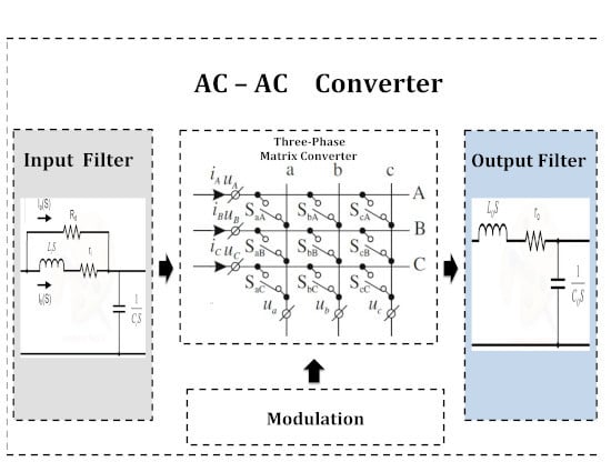
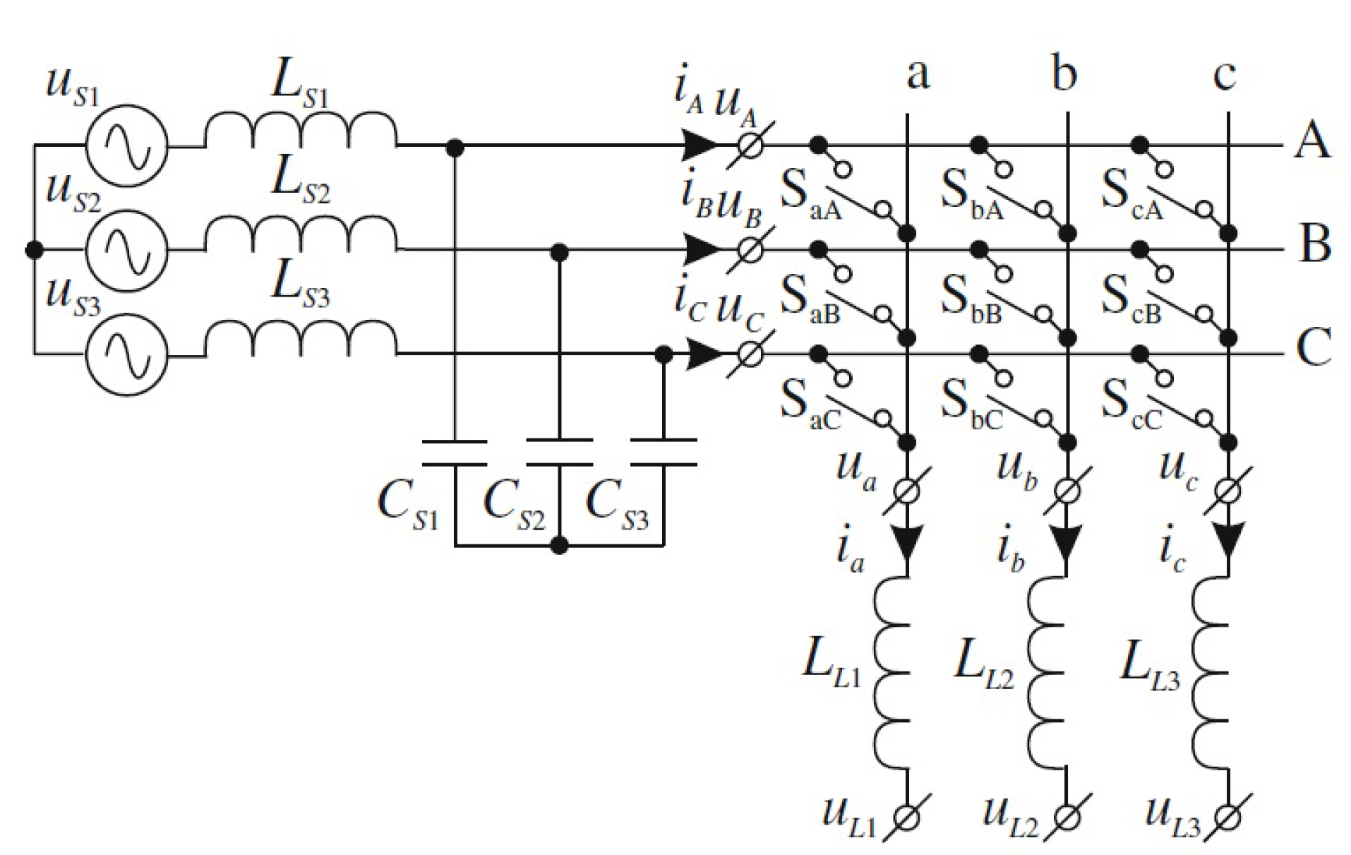
2. Matrix Converter
- The waveform of the input current is sinusoidal, and this allows minimizing the harmonic and subharmonic content injected by the converter into the AC power supply.
- The energy flow can be bidirectional.
- The minimum requirement of passive components, which implies a reduction of their resignations by up to 50% compared to other converter topologies.
- Power-factor control.
- Complex implementation.
- It requires bidirectional switches, so the number of electronic devices in the switching matrix increases, depending on the number of stands and outputs.
- It presents a problem of both synchronization and protection.
- In open loop operation, there is distortion of the input and output waveforms due to the high sensitivity of the converter.
- The maximum voltage ratio is .
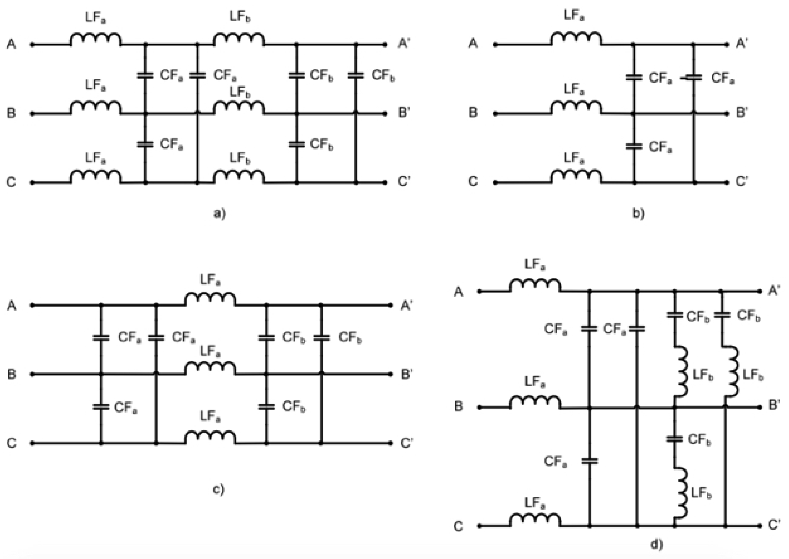
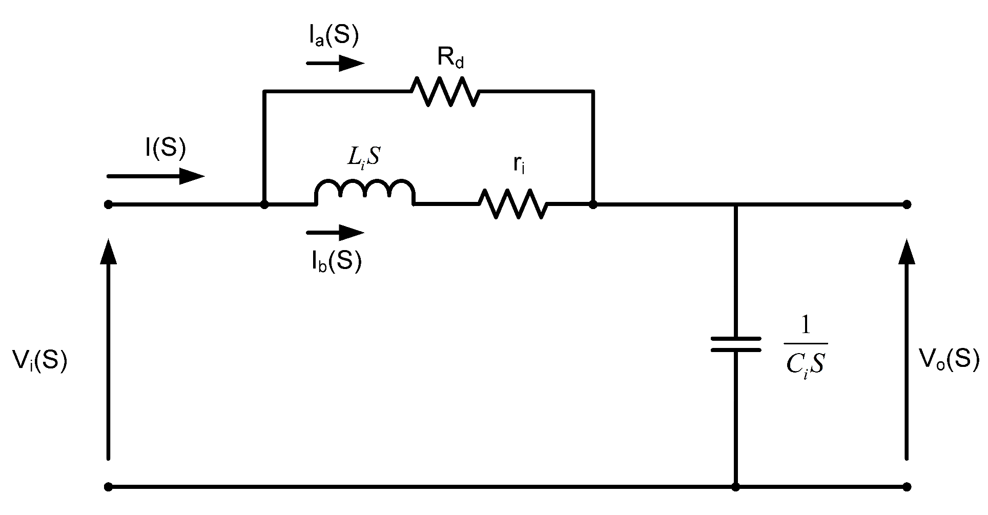
3. Input Filter
- : Limits the over-voltages of the input originated by the distortions or disturbances of the power supply network. The parasitic inductances through the switches of the MC can generate over-voltages on both sides of the converter due to the high values of in the switching periods. To reduce this effect, capacitor should be placed as close as possible to the MC switches.
- : The switching process in the MC causes the appearance of over-currents, which are generated from small discontinuities that occur when switching from a switch on an input phase to another switch on a different input phase. The inductor is responsible for smoothing the slope of that over-current.
Input Filter Optimization
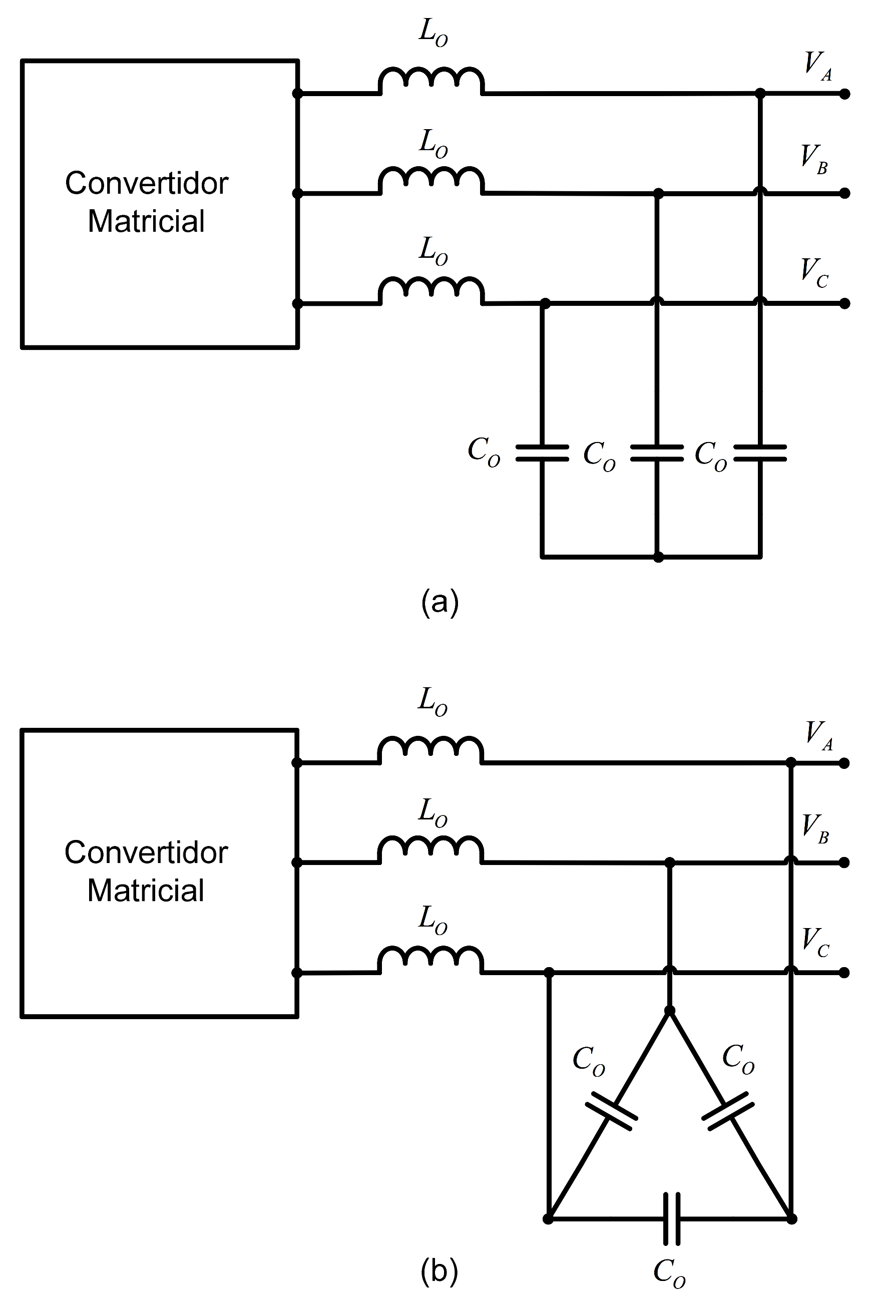
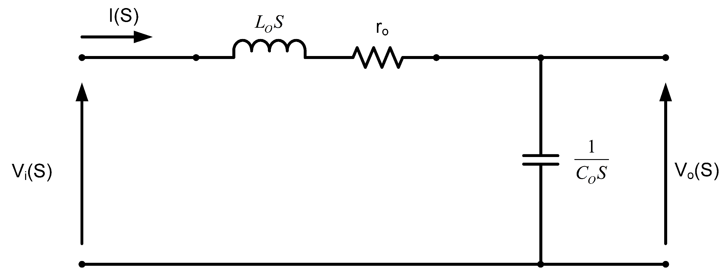
4. Output Filter
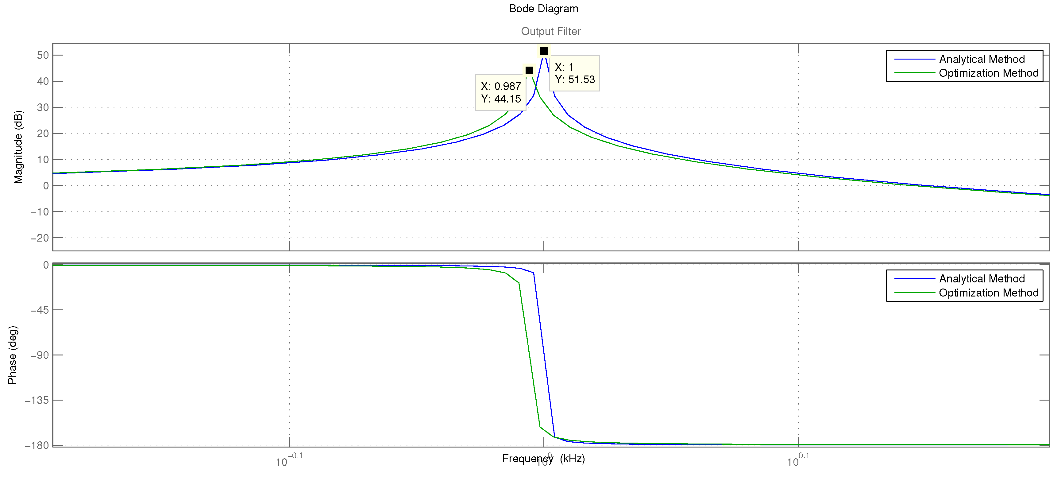
Output Filter Optimization
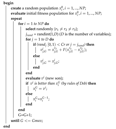
5. Differential Evolution
- Between two feasible individuals, the one with the best aptitude is selected.
- Between a feasible individual and an unfeasible one, the feasible one is selected.
- Between two non-feasible individuals, the one that least violates the sum of constraints is selected.
| Algorithm 1: Differential evolution. |
 |
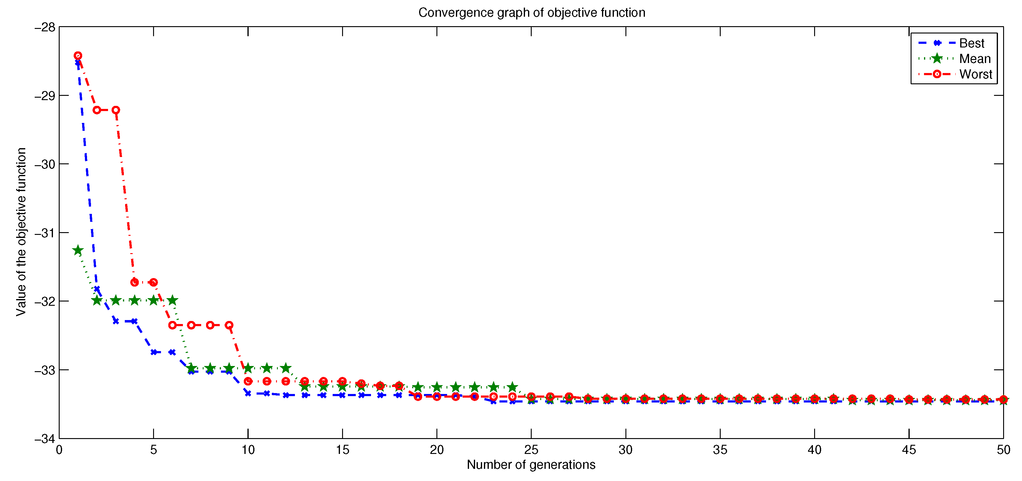
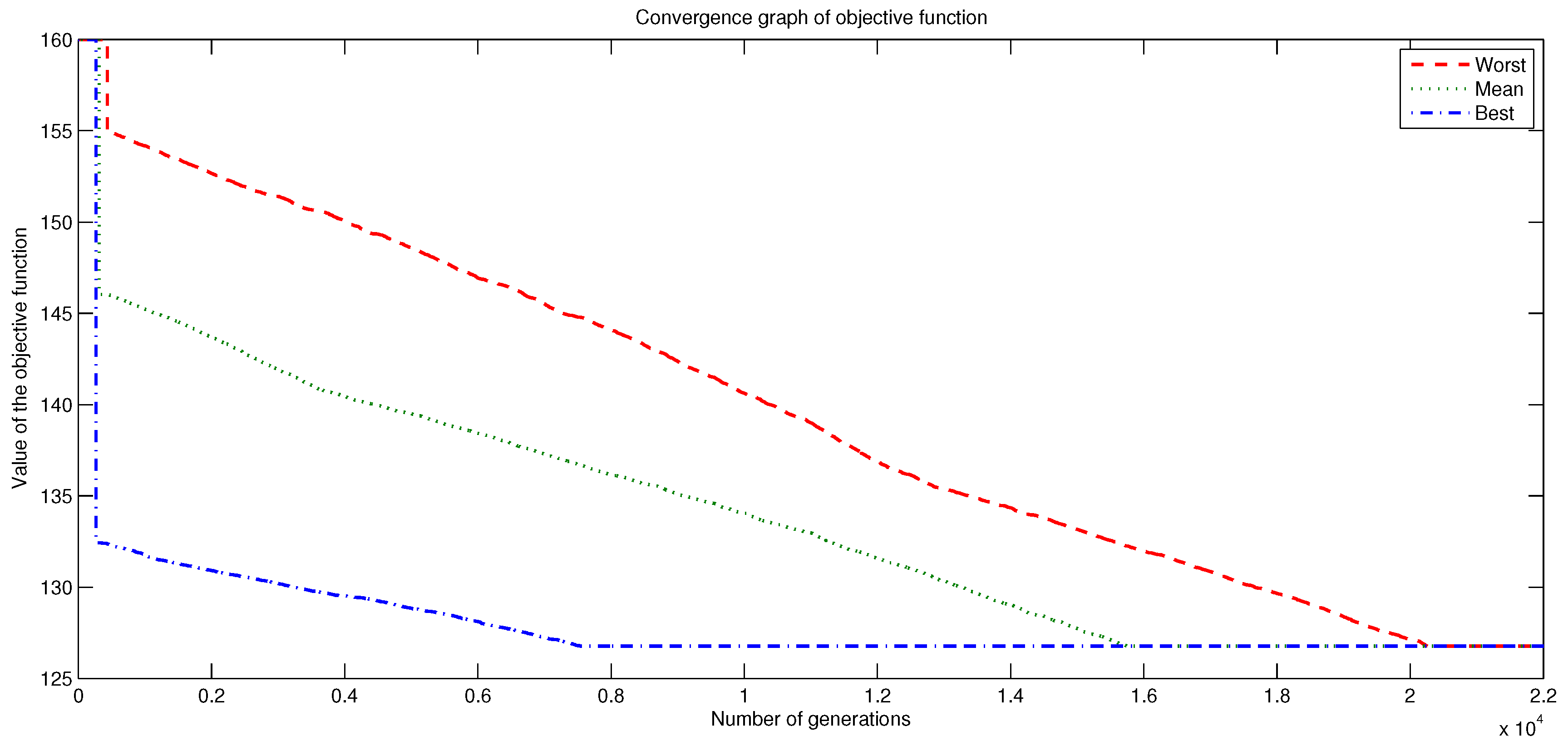
6. Results
6.1. Optimal Solutions
- Design variables: 3
- Individuals: 50
- Generations: 500
- Mutation factor: random from to
- Cross factor: random from to
- Design variables: 4
- Individuals: 20
- Generations: 30,000
- Mutation factor: random from to
- Cross factor: random from to
6.2. Stability
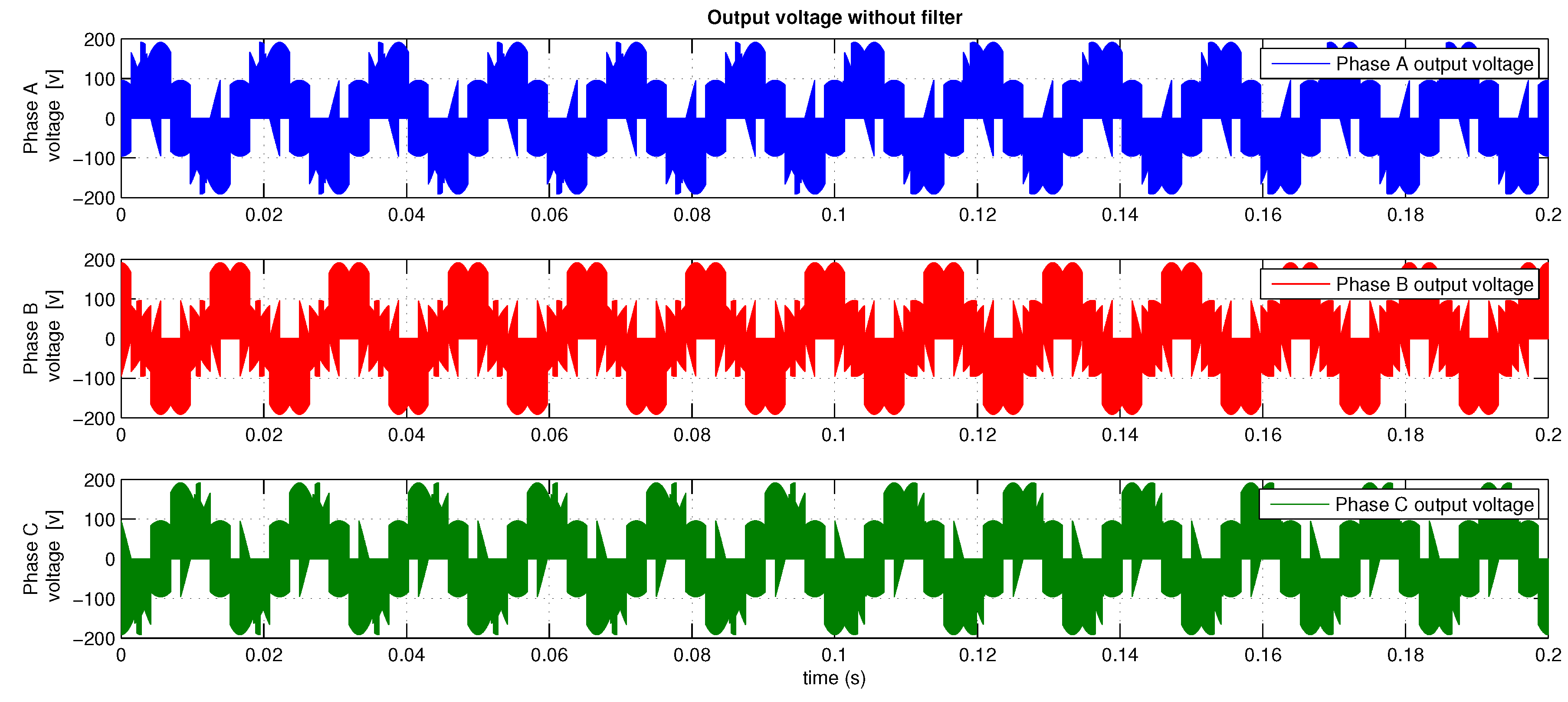
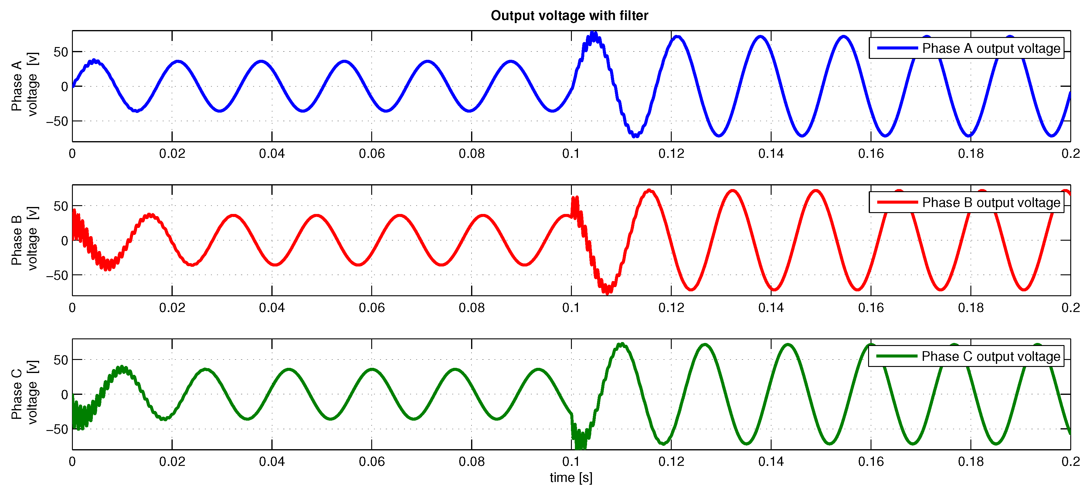
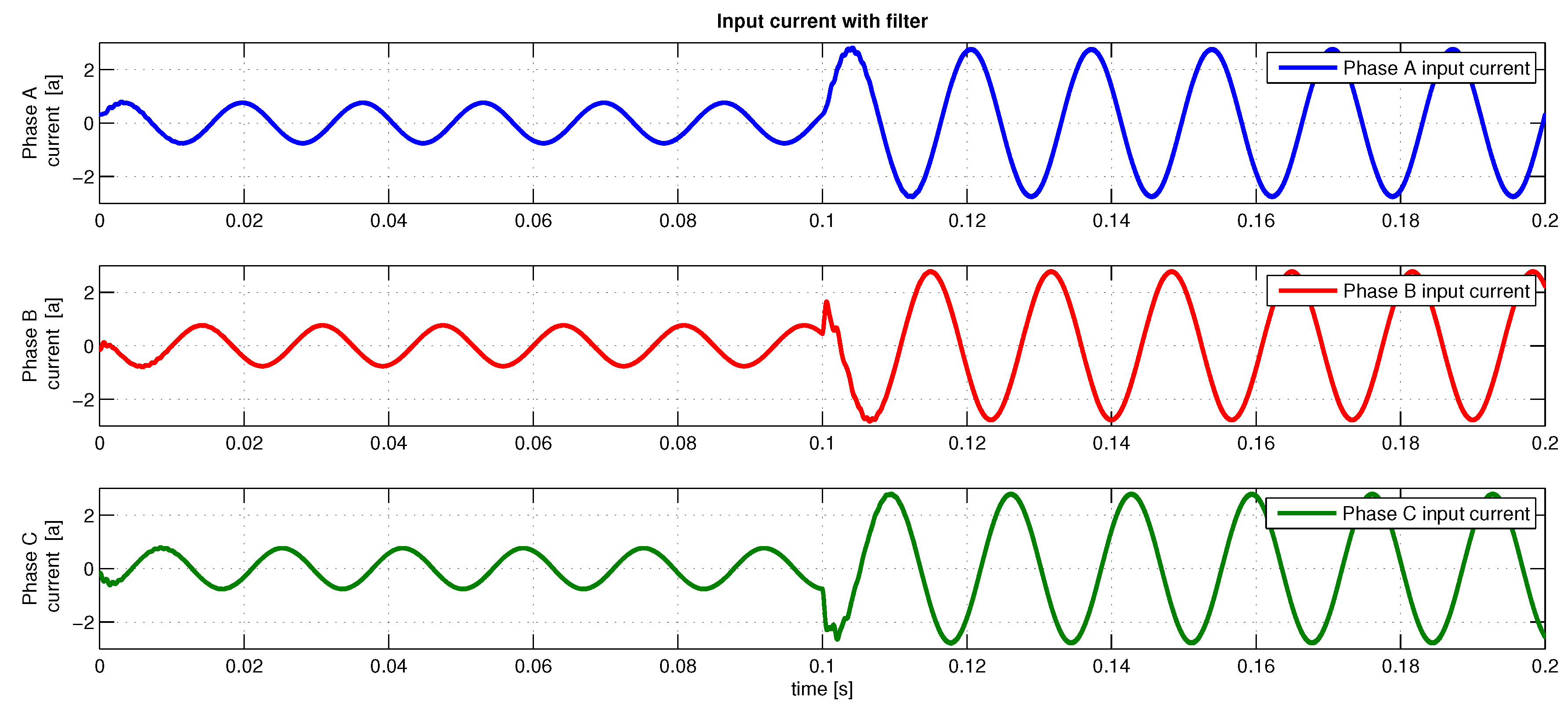
6.3. Simulations
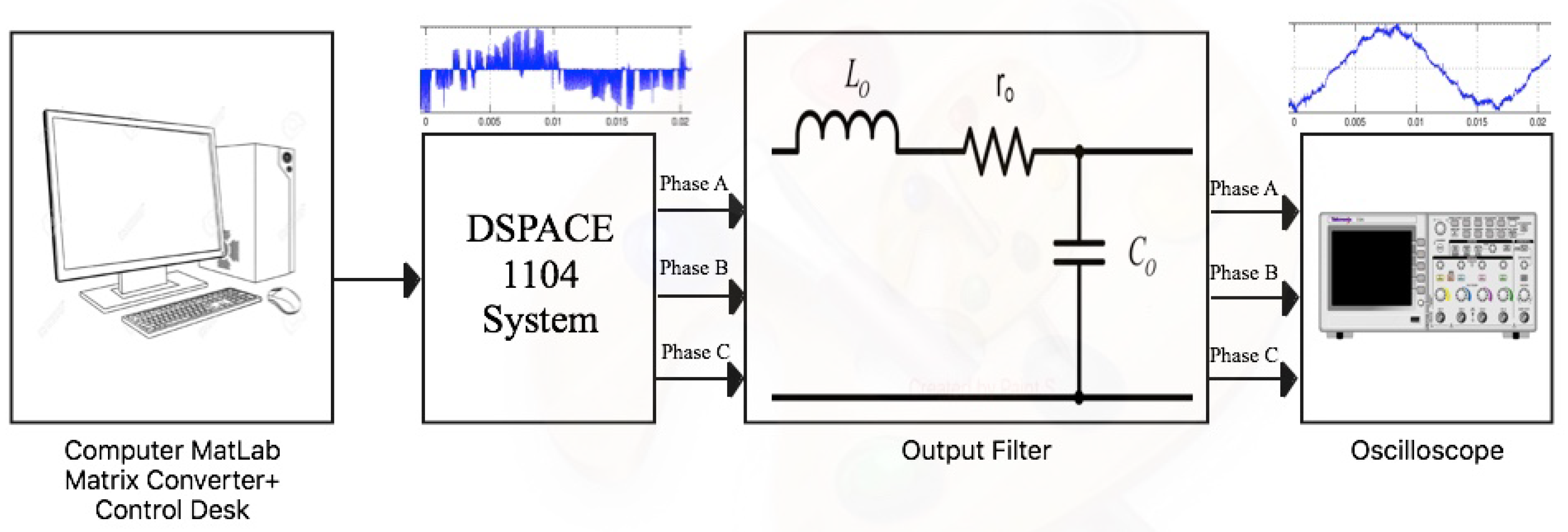
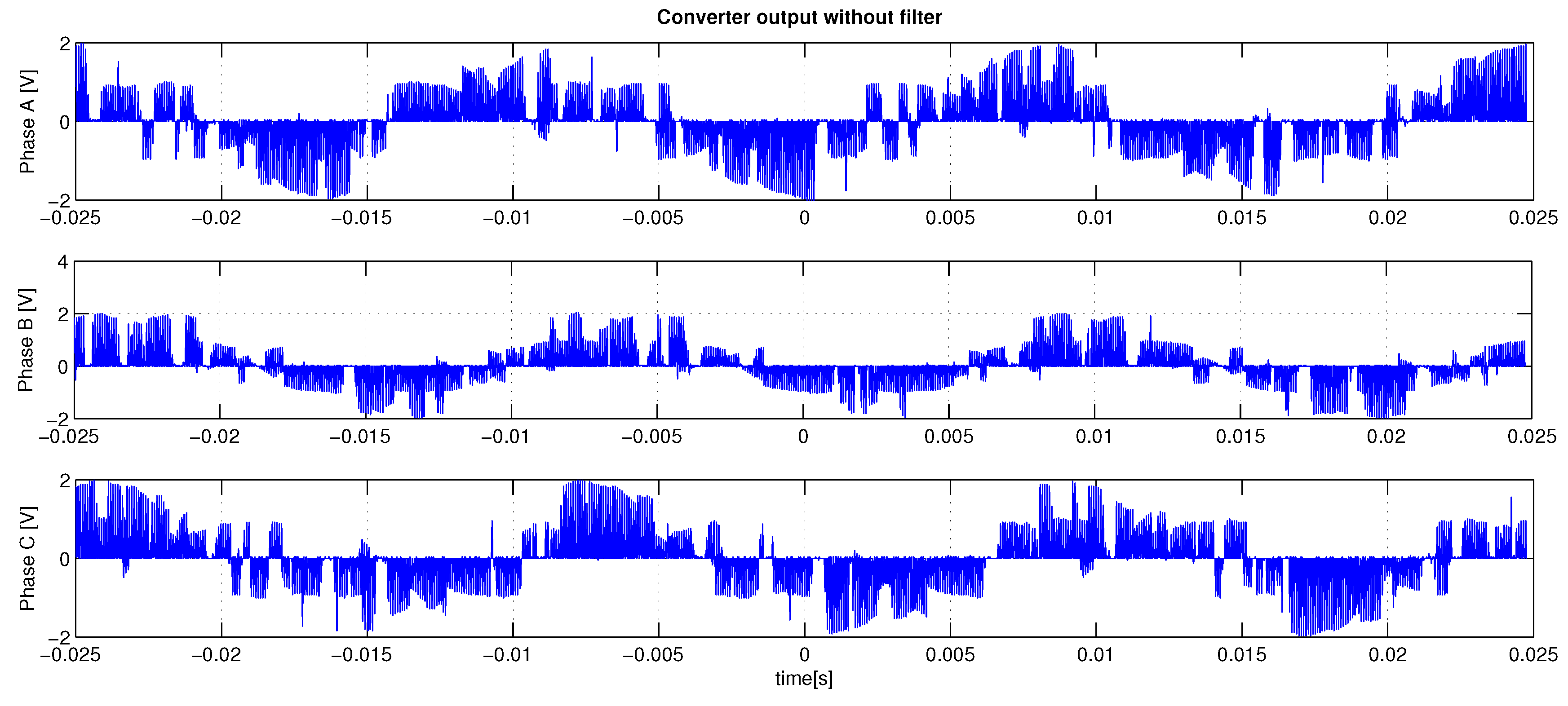
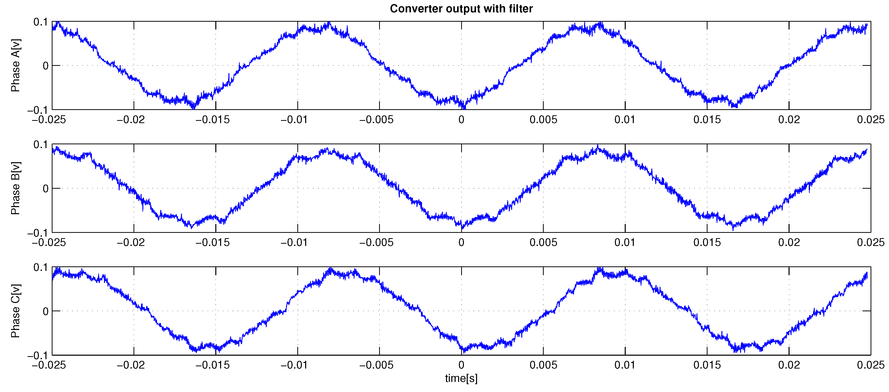
6.4. Experimental Result
7. Conclusions
Author Contributions
Funding
Acknowledgments
Conflicts of Interest
Abbreviations
| MC | Matrix Converter |
| SVM | Spatial Vector Modulation |
| DE | Differential Evolution |
| PWM | Pulse Width Modulation |
| AC | Alternating Current |
| PF | Power Factor |
Appendix A. Nomenclature
| Resonance frequency of the input filter | |
| Capacitive reactive power | |
| Input capacitance | |
| Input inductance | |
| Input inductance resistance | |
| Damping resistance | |
| Input RMS voltage | |
| Nominal power | |
| Angular frequency | |
| Power frequency of the input source | |
| Frequency of change | |
| Natural frequency | |
| Buffer factor of the input filter | |
| Output capacitance | |
| Output inductance | |
| Output inductance resistance | |
| Resonance frequency of the output filter | |
| Output frequency of converter | |
| Buffer factor of the output filter | |
| Crossover factor | |
| F | Mutation factor |
| Population of individuals |
References
- Rodriguez, J.; Rivera, M.; Kolar, J.W.; Wheeler, P.W. A review of control and modulation methods for matrix converters. IEEE Trans. Ind. Electron. 2012, 59, 58–70. [Google Scholar] [CrossRef]
- Venturini, M.; Alesina, A. The generalised transformer: A new bidirectional, sinusoidal waveform frequency converter with continuously adjustable input power factor. In Proceedings of the Power Electronics Specialists Conference, Atlanta, GA, USA, 16–20 June 1980; IEEE: Piscataway, NJ, USA, 1980; pp. 242–252. [Google Scholar]
- Alesina, A.; Venturini, M. Solid-state power conversion: A Fourier analysis approach to generalized transformer synthesis. IEEE Trans. Circuits Syst. 1981, 28, 319–330. [Google Scholar] [CrossRef]
- Alesina, A.; Venturini, M. Intrinsic amplitude limits and optimum design of 9-switches direct PWM AC-AC converters. In Proceedings of the PESC’88 Record, 19th Annual IEEE Power Electronics Specialists Conference 1988, Kyoto, Japan, 11–14 April 1988; IEEE: Piscataway, NJ, USA, 1988; pp. 1284–1291. [Google Scholar]
- Alesina, A.; Venturini, M.G. Analysis and design of optimum-amplitude nine-switch direct AC-AC converters. IEEE Trans. Power Electron. 1989, 4, 101–112. [Google Scholar] [CrossRef]
- Wheeler, P.W.; Rodriguez, J.; Clare, J.C.; Empringham, L.; Weinstein, A. Matrix converters: A technology review. IEEE Trans. Ind. Electron. 2002, 49, 276–288. [Google Scholar] [CrossRef]
- Rodriguez, J. A new control technique for AC-AC converters. In Proceedings of the IFAC Control in Power Electronics and Electrical Drives Conference, Lausanne, Switzerland, 12–14 September 1983; Elsevier: Amsterdam, The Netherlands, 1983; pp. 203–208. [Google Scholar]
- Ziogas, P.D.; Khan, S.I.; Rashid, M.H. Some improved forced commutated cycloconverter structures. IEEE Trans. Ind. Appl. 1985, IA-21, 1242–1253. [Google Scholar] [CrossRef]
- Ziogas, P.D.; Khan, S.I.; Rashid, M.H. Analysis and design of forced commutated cycloconverter structures with improved transfer characteristics. IEEE Trans. Ind. Electron. 1986, IE-33, 271–280. [Google Scholar] [CrossRef]
- Roy, G.; Duguay, L.; Manias, S.; April, G. Asynchronous operation of cycloconverter with improved voltage gain by employing a scalar control algorithm. In IEEE IAS Conference Record 1987; IEEE: Piscataway, NJ, USA, 1987; pp. 889–898. [Google Scholar]
- Roy, G.; April, G.E. Cycloconverter operation under a new scalar control algorithm. In Proceedings of the PESC’89 Record, 20th Annual IEEE Power Electronics Specialists Conference, Milwaukee, WI, USA, 26–29 June 1989; IEEE: Piscataway, NJ, USA, 1989; pp. 368–375. [Google Scholar]
- Roy, G.; April, G.E. Direct frequency changer operation under a new scalar control algorithm. IEEE Trans. Power Electron. 1991, 6, 100–107. [Google Scholar] [CrossRef]
- Ishiguro, A.; Furuhashi, T.; Okuma, S. A novel control method for forced commutated cycloconverters using instantaneous values of input line-to-line voltages. IEEE Trans. Ind. Electron. 1991, 38, 166–172. [Google Scholar] [CrossRef]
- Huber, L.; Borojevic, D.; Burany, N. Voltage space vector based PWM control of forced commutated cycloconverters. In Proceedings of the IECON’89, 15th Annual Conference of IEEE Industrial Electronics Society, Philadelphia, PA, USA, 6–10 November 1989; IEEE: Piscataway, NJ, USA, 1989; pp. 106–111. [Google Scholar]
- Huber, L.; Borojevic, D. Space vector modulated three-phase to three-phase matrix converter with input power factor correction. IEEE Trans. Ind. Appl. 1995, 31, 1234–1246. [Google Scholar] [CrossRef]
- Casadei, D.; Serra, G.; Tani, A.; Zarri, L. Matrix converter modulation strategies: A new general approach based on space-vector representation of the switch state. IEEE Trans. Ind. Electron. 2002, 49, 370–381. [Google Scholar] [CrossRef]
- Pinto, F.; Silva, F. Sliding mode control of space vector modulated matrix converter with sinusoidal input/output waveforms and near unity input power factor. In Proceedings of the 8th European Conference on Power Electronics and Applications, Lausanne, Switzerland, 7–9 September 1999; Volume 99, pp. 1–9. [Google Scholar]
- Yoon, Y.D.; Sul, S.K. Carrier-based modulation technique for matrix converter. IEEE Trans. Power Electron. 2006, 21, 1691–1703. [Google Scholar] [CrossRef]
- Andreu, J.; de Alegria, I.M.; Kortabarria, I.; Martin, J.L.; Ceballos, S. Improvement of the Matrix Converter Start-up Process. In Proceedings of the IECON 2007, 33rd Annual Conference of the IEEE Industrial Electronics Society, Taipei, Taiwan, 5–8 November 2007; IEEE: Piscataway, NJ, USA, 2007; pp. 1811–1816. [Google Scholar]
- Erdem, E.; Tatar, Y.; Sünter, S. Effects of input filter on stability of matrix converter using venturini modulation algorithm. In Proceedings of the 2010 International Symposium of the Power Electronics Electrical Drives Automation and Motion (SPEEDAM), Pisa, Italy, 14–16 June 2010; IEEE: Piscataway, NJ, USA, 2010; pp. 1344–1349. [Google Scholar]
- Wheeler, P.; Grant, D. Optimised input filter design and low-loss switching techniques for a practical matrix converter. IEE Proc. Electr. Power Appl. 1997, 144, 53–60. [Google Scholar] [CrossRef]
- Klumpner, C.; Nielsen, P.; Boldea, I.; Blaabjerg, F. A new matrix converter motor (MCM) for industry applications. IEEE Trans. Ind. Electron. 2002, 49, 325–335. [Google Scholar] [CrossRef]
- Fnaiech, F.; Al-Haddad, K. Input filter design for SVM dual-bridge matrix converters. In Proceedings of the 2006 IEEE International Symposium of the Industrial Electronics, Montreal, QC, Canada, 9–13 July 2006; IEEE: Piscataway, NJ, USA, 2006; Volume 2, pp. 797–802. [Google Scholar]
- Kume, T.; Yamada, K.; Higuchi, T.; Yamamoto, E.; Hara, H.; Sawa, T.; Swamy, M.M. Integrated filters and their combined effects in matrix converter. IEEE Trans. Ind. Appl. 2007, 43, 571–581. [Google Scholar] [CrossRef]
- Friedli, T.; Kolar, J.W.; Rodriguez, J.; Wheeler, P.W. Comparative evaluation of three-phase AC–AC matrix converter and voltage DC-link back-to-back converter systems. IEEE Trans. Ind. Electron. 2012, 59, 4487–4510. [Google Scholar] [CrossRef]
- Trentin, A.; Zanchetta, P.; Clare, J.; Wheeler, P. Automated optimal design of input filters for direct ac/ac matrix converters. IEEE Trans. Ind. Electron. 2012, 59, 2811–2823. [Google Scholar] [CrossRef]
- BoussaïD, I.; Lepagnot, J.; Siarry, P. A survey on optimization metaheuristics. Inf. Sci. 2013, 237, 82–117. [Google Scholar] [CrossRef]
- Storn, R.; Price, K. Differential evolution—A simple and efficient heuristic for global optimization over continuous spaces. J. Glob. Optim. 1997, 11, 341–359. [Google Scholar] [CrossRef]
- Mezura-Montes, E.; Coello Coello, C.; Velázquez-Reyes, J.; Muñoz-Dávila, L. Multiple trial vectors in differential evolution for engineering design. Eng. Optim. 2007, 39, 567–589. [Google Scholar] [CrossRef]
- Ameca-Alducin, M.Y.; Mezura-Montes, E.; Cruz-Ramírez, N. Dynamic differential evolution with combined variants and a repair method to solve dynamic constrained optimization problems: An empirical study. Soft Comput. 2018, 22, 541–570. [Google Scholar] [CrossRef]
- Pinto, S.F.; Silva, J.F. Input filter design for sliding mode controlled matrix converters. In Proceedings of the 2001 IEEE 32nd Annual Power Electronics Specialists Conference (PESC), Vancouver, BC, Canada, 17–21 June 2001; IEEE: Piscataway, NJ, USA, 2001; Volume 2, pp. 648–653. [Google Scholar]
- She, H.; Lin, H.; Wang, X.; Yue, L. Damped input filter design of matrix converter. In Proceedings of the International Conference of the Power Electronics and Drive Systems (PEDS), Taipei, Taiwan, 2–5 November 2009; IEEE: Piscataway, NJ, USA, 2009; pp. 672–677. [Google Scholar]
- Dewan, S.; Ziogas, P. Optimum filter design for a single-phase solid-state UPS system. IEEE Trans. Ind. Appl. 1979, IA-15, 664–669. [Google Scholar] [CrossRef]
- Steinke, J.K. Use of an LC filter to achieve a motor-friendly performance of the PWM voltage source inverter. IEEE Trans. Energy Convers. 1999, 14, 649–654. [Google Scholar] [CrossRef]
- Kim, H.; Sul, S.K. Analysis on output LC filters for PWM inverters. In Proceedings of the IPEMC’09, IEEE 6th International Power Electronics and Motion Control Conference, Wuhan, China, 17–20 May 2009; IEEE: Piscataway, NJ, USA, 2009; pp. 384–389. [Google Scholar]
- Kim, J.; Choi, J.; Hong, H. Output LC filter design of voltage source inverter considering the performance of controller. In Proceedings of the PowerCon 2000, International Conference on Power System Technology, Perth, Australia, 4–7 December 2000; IEEE: Piscataway, NJ, USA, 2000; Volume 3, pp. 1659–1664. [Google Scholar]
- Deb, K. An efficient constraint handling method for genetic algorithms. Comput. Methods Appl. Mech. Eng. 2000, 186, 311–338. [Google Scholar] [CrossRef]
- Eiben, Á.E.; Hinterding, R.; Michalewicz, Z. Parameter control in evolutionary algorithms. IEEE Trans. Evol. Comput. 1999, 3, 124–141. [Google Scholar] [CrossRef] [Green Version]
- Rohouma, W.M.; Arevalo, S.L.; Zanchetta, P.; Wheeler, P. Repetitive Control for a Four Leg Matrix Converter. In Proceedings of the 5th IET International Conference on Power Electronics, Machines and Drives (PEMD 2010), Brighton, UK, 19–21 April 2010; IET: Brighton, UK, 2010. [Google Scholar]
- Rohouma, W.M.; de Lillo, L.; Lopez, S.; Zanchetta, P.; Wheeler, P.W. A single loop repetitive voltage controller for a four legs matrix converter ground power unit. In Proceedings of the 2011—14th European Conference on Power Electronics and Applications (EPE 2011), Birmingham, UK, 30 August–1 September 2011; IEEE: Piscataway, NJ, USA, 2011; pp. 1–9. [Google Scholar]


| Parameter | Objective Function (dB) |
|---|---|
| Best | |
| Worst | |
| Average | |
| Standard deviation | |
| Variance |
| (Hz) | |||
|---|---|---|---|
| 1000 | |||
| 1000 | |||
| 1000 | |||
| 1000 | |||
| 1000 | |||
| 1000 | |||
| 1000 | |||
| 1000 | |||
| 1000 | |||
| 1000 | |||
| 1000 | |||
| 1000 | |||
| 1000 | |||
| 1000 | |||
| 1000 | |||
| 1000 | |||
| 1000 | |||
| 1000 | |||
| 1000 | |||
| 1000 | |||
| 1000 | |||
| 1000 | |||
| 1000 | |||
| 1000 | |||
| 1000 | |||
| 1000 | |||
| 1000 | |||
| 1000 |
| Parameters | Objective Function (dB) |
|---|---|
| Best | |
| Worst | |
| Average | |
| Standard deviation | |
| Variance |
© 2020 by the authors. Licensee MDPI, Basel, Switzerland. This article is an open access article distributed under the terms and conditions of the Creative Commons Attribution (CC BY) license (http://creativecommons.org/licenses/by/4.0/).
Share and Cite
Muñoz-Castillo, J.; Muñoz-Hernández, G.A.; Portilla-Flores, E.A.; Vega-Alvarado, E.; Calva-Yáñez, M.B.; Mino-Aguilar, G.; Niño-Suarez, P.A. Design of the Input and Output Filter for a Matrix Converter Using Evolutionary Techniques. Appl. Sci. 2020, 10, 3524. https://doi.org/10.3390/app10103524
Muñoz-Castillo J, Muñoz-Hernández GA, Portilla-Flores EA, Vega-Alvarado E, Calva-Yáñez MB, Mino-Aguilar G, Niño-Suarez PA. Design of the Input and Output Filter for a Matrix Converter Using Evolutionary Techniques. Applied Sciences. 2020; 10(10):3524. https://doi.org/10.3390/app10103524
Chicago/Turabian StyleMuñoz-Castillo, Joel, Germán Ardul Muñoz-Hernández, Edgar Alfredo Portilla-Flores, Eduardo Vega-Alvarado, Maria Bárbara Calva-Yáñez, Gerardo Mino-Aguilar, and Paola Andrea Niño-Suarez. 2020. "Design of the Input and Output Filter for a Matrix Converter Using Evolutionary Techniques" Applied Sciences 10, no. 10: 3524. https://doi.org/10.3390/app10103524
APA StyleMuñoz-Castillo, J., Muñoz-Hernández, G. A., Portilla-Flores, E. A., Vega-Alvarado, E., Calva-Yáñez, M. B., Mino-Aguilar, G., & Niño-Suarez, P. A. (2020). Design of the Input and Output Filter for a Matrix Converter Using Evolutionary Techniques. Applied Sciences, 10(10), 3524. https://doi.org/10.3390/app10103524