Technology Mapping of FSM Oriented to LUT-Based FPGA


Department of Digital Systems, Silesian University of Technology, ul. Akademicka 2A, 44-100 Gliwice, Poland
*
Author to whom correspondence should be addressed.
Appl. Sci. 2020, 10(11), 3926; https://doi.org/10.3390/app10113926
Submission received: 5 May 2020
/
Revised: 27 May 2020
/
Accepted: 3 June 2020
/
Published: 5 June 2020
(This article belongs to the Special Issue Finite State Machines: Theory, Design and Applications)
Abstract
:The main purpose of the paper is to present technology mapping of FSM (finite state machine) oriented to LUT (look-up table)-based FPGA (field-programmable gate array). The combinational part of an automaton, which consists of a transition block and an output block, was mapped in LUT-based logic blocks. In the paper, the idea of carrying out the combinational part of FSM was presented and leads to the reduction of the number of LUTs needed to carry out an automaton. The essence of this method is a simultaneous synthesis of the whole combinational block described in the form of multi-output function. The proposed idea makes it possible to conduct decomposition that may enable to share logic blocks, which can lead to the reduction of using resources of FPGA. The decomposition process was conducted using the analyzed DECOMP system. The effectiveness of the proposed idea of the FSM description was also confirmed by conducting decomposition with the usage of the ABC system. The obtained results prove the efficiency of the proposed synthesis method of FSM in comparison with the separate synthesis of a transition block and an output block.

1. Introduction
Logic synthesis algorithms targeted at programmable logic devices are extremely important. Their effectiveness leads to obtaining solutions: faster, cheaper, whose power consumption has been significantly reduced. This is particularly important in the case of sequential circuits where FSM (finite state machine) plays a key role. The process of carrying out FSM in programmable logic devices is associated with the problem of an efficient technology mapping. The state assignment has a substantial influence on technology mapping. Technology mapping is usually oriented at precisely described project limitations. The goal of optimization may be the area [1,2], the speed [3], and minimization of the power consumption [4,5] or testability of a circuit [6].
The state assignment is the most important element of FSMs synthesis. Despite the fact that advanced methods of state assignment [7,8] are often regarded as optimal, more effective methods of carrying out FSM have been still searched for [9,10,11,12,13,14]. The problem of state assignment is often reduced to i.e., input and output coding [15]. Some known methods are based on dichotomies [16], adjacency analysis [17], or dominance graphs [18]. In recent years, the problem of the synthesis of low-power circuits has been the matter of the main interest. Classic methods of coding directed at minimization of the power consumption are based on minimization of the switching activity. The codes with minimum code distance are assigned to the states and transitions occur between them [19,20,21] (minimum weighted hamming distance method). There are also well-known coding methods that are based on integer linear programming [19] and those that use genetic algorithms [22,23]. However, the most popular state coding methods include those using heuristic methods [24,25]. A series of methods of carrying out FSM are also very well-known and the essence lies in the usage of various solutions enabling to limit the power consumption by local lowering of both power supply as well as clock frequency signals. In many cases, the main idea of FSM logic synthesis is based on decomposition. Different kinds of decomposition are considered such as structural decomposition of FSMs [11,26,27,28], functional decomposition [29,30,31], or general decomposition [22]. The decomposition-based logic synthesis is especially crucial in the case of LUT-based (look-up table) FPGAs (field-programmable gate array). The complexity of synthesis led to searching for new forms of FSM specification. The most promising are binary decision diagrams (BDD) [32,33] and and-inverter graphs (AIG) [34]. Binary decision diagrams as well as and-inverter graphs, implemented in the tool ABC [35], may be used in the synthesis of FSMs. The process of synthesis can be also directed at using inbuilt memory blocks [36]. A special place is dedicated to the methods enabling to carry out circuits in the form of asynchronous circuits [37] or GALS structures (globally asynchronous locally synchronous) [38]. A logic synthesis is also especially essential from the point of view of designing cyber-physical systems [39,40,41,42].
It should be mentioned that skillful coding of states does not solve all the problems enabling for effective mapping of FSM in a programmable structure. It is also worth to mention that in commercial tools, the most basic methods of coding the states such as ‘one-hot’ encoding or binary encoding are used. The solutions, obtained this way, are usually far from optimal. In the case of carrying out FSM in LUT-based FPGAs, decomposition is an especially crucial element of the logic synthesis. It is a theoretical basis of mapping of logic functions into LUTs [43]. A series of various decomposition strategies are known [44]. In the process of decomposition, multi-output functions decomposition should be considered as it gives the possibility to search for shared LUTs. This type of attitude connected with a skillful unicoding leads to more efficient solutions than decomposing of each function separately. The above observations are the source of inspiration to search for the method of a simultaneous synthesis of combinational FSM blocks that have to be effectively mapped into LUT-based FPGA.
The goal of the paper is to present synthesis methods of FSM dedicated to LUT-based FPGAs, whose essence is based on a simultaneous synthesis of a transition block and an output block, enabling for effective decomposition process. The process of decomposition is based on the method of evaluating the efficiency of technology mapping that is known from literature. The method uses triangle tables which are directed at optimization of a decomposition of a multi-output function.
In comparison with the earlier works of the authors, an innovative element of this work is the introduction of a method for estimating the technology mapping of entire multi-output function using previously known triangle tables. Appropriate multi-output function is created taking into account sharing of resources through various combination blocks that are part of FSM. The object of interest is FSM, for which an innovative combination of the concept of joint implementation of FSM combination blocks known from the literature has been proposed with our concept of effective implementation of multi-output function, tailored to the internal resources of the structure used.
2. Theoretical Background
FSM is an abstract mathematical model of a sequential circuit. This model is a five-tuple: {X,Y,S,S0,δ,λ}, where X is a set of input vectors, S—the set of internal states, S0—initial state, and Y—the set of output vectors. The relations between these elements are determined by a transition function, usually marked with the symbol δ, and an output function (λ) describing the values of output signals. A general structure of FSM is shown in Figure 1. Transition and output functions are associated with combinational blocks marked δ and λ, respectively. A memory block was symbolically marked as DFF (D-type flip-flop) in Figure 1.
In accordance with the designations, included in Figure 1, a transition function is determined by δ: BN+K → BK, where B = {0,1}. Depending on a type of automaton λ: BK → BM (Moore’s automaton) or λ: BN+K → BM (Mealy’s automaton). In the process of coding states, each internal state of an automaton is associated with K-bit vector of a state. The number of a state vector’s bits depends on the accepted method of coding internal states and fulfills the inequality ⌈lg2(card(S))⌉ ≤ K ≤ card(S) [13].
Logic blocks, included in FPGAs, contain necessary resources needed to carry out FSM. A memory block includes D flip-flops placed in logic blocks. The number of flip-flops depends on the state assignment. The transition and output blocks are carried out using LUTs whose outputs may be directly joined to the inputs of D flip-flops. One vital feature of LUTs is the fact that they enable to carry out any function that has a limited (usually low) number of variables. A low number of inputs of LUTs requires a multilevel carrying out of a combinational logic in the form of the net of LUTs. Decomposition is a mathematical model of a partition that is a basis of mapping of a logic function into LUT-based FPGAs.
A decomposition model, which is the basis of the series of synthesis strategies, relies on the theorem by Ashenhurst–Curtis [45,46].
Let f be n-input and m-output logic function reflecting Bn set into Bm set i.e., f: Bn → Bm, where B = {0,1}. Function f: Bn → Bm may be presented as Y = {ym−1, …, y1, y0} = f(In−1, …, I1, I0).
Function f: Bn → Bm is subjected to decomposition i.e.:
if and only if column multiplicity of Karnaugh map υ(Xf | Xb) ≤ 2p.
f(Xf,Xb) = F[g1(Xb), g2(Xb), …, gp(Xb), Xf],
The sets Xb and Xf are called a bound and a free set, respectively, where Xb ∪ Xf = {In−1, …, I1, I0} and Xb ∩ Xf = Φ.
The above theorem is a mathematical model of technology mapping of a function f: Bn → Bm in two LUTs: LUT_card(Xb)/p and LUT_card(Xf)+p/m, where LUT_a/b is the block that is a-inputs and b-outputs (Figure 2).
The partition of a circuit is implied from the partition of variables. One part of n-input variables is the set of variables for p bound functions carried out in a bound block. The rest of the part of the variables creates a free set. From technology mapping of multi-output function point of view, it is key for LUT_k/x blocks that card(Xb) ≤ k and card(Xf) + p ≤ k, where k indicates the number of inputs of LUT.
The choice of an appropriate partition of variables is not so simple. It is directly connected with the choice of a decomposition path. In the process of searching for decomposition, various partitions are considered for which column multiplicity of a partitions’ matrix is determined. Using binary decision diagrams, column multiplicity may be determined by defining so called number of cut nodes [47]. It shall be noticed that in i-step, there is a necessity to choose one partition (one decomposition) that is the essence of the best mapping of the analyzed function. In the process of choosing an appropriate decomposition, it is worth to take into account configurable abilities of logic blocks included in FPGA.
Let us consider the choice of decomposition of the multi-output function in the block that may be configured as LUT_5/1 or LUT_4/2. Let us assume that while analyzing various partitions of variables, four different partitions were found. They are characterized by ordered pairs of numbers (card(Xb),p) that have the values (4,3), (4,2), (5,3), and (5,4), respectively. The question is, which partition of variables is the most efficient in the situation when we want to use the blocks LUT_5/1 or LUT_4/2. In order to limit the number of inputs to maximum in i-step of decomposition, it is advantageous to use the solution for which card(Xb) − p takes the maximum value. In this situation, it is better to choose one of two decompositions characterized by the ordered pair (card(Xb),p) equal (4,2) or (5,3). Assuming the possibility of configuration of LUTs to the form of LUT_4/2 or LUT_5/1, the most effective decomposition is (card(Xb),p) = (4,2) as it requires using only one LUT_4/2 block. Decomposition, for which (card(Xb),p) = (5,3) forces using up to three blocks LUT_5/1.
The above considerations enable to form the rule of the choice of decomposition in i-step which is based on the choice of the solution for which the cofactor:
takes the maximum value.
δ = Number_of_blocks − (card(Xb) − p),
The values of the cofactor δ directly depend on card(Xb), p, and additionally configurable abilities of LUTs. The choice of configuration of a logic block should be carried out in the way to use minimum number of configurable logic blocks.
In the process of searching for the best mapping, appears the problem of choosing an appropriate decomposition. The choice of an appropriate decomposition is based on the choice of the minimum value of the cofactor δ whose values are included in separate cells of a triangle table (Figure 3) [48]. The values of the cofactor δ are indicated in accordance with the dependency (2). Configurable abilities of LUTs to one of two forms LUT_5/1 or LUT_4/2 are taken into account.
The process of choosing an appropriate decomposition in i-stage of mapping enables to create appropriate paths leading to very effective solutions taking area into account [47]. Ashenhurst–Curtis decomposition (often named as a simple serial decomposition) is the basis of more complex decomposition models such as iterative, multiple, and mixed decomposition [43,46].
Implemented combinational circuits are usually multi-output. Thus, it is key to determine the effectiveness of mapping for a multi-output function.
3. Indicating the Efficiency of Mapping for a Multi-Output Function
A structure carrying out a multi-output function in FPGA structures may be characterized by existing two types of logic resources: shared and non-shared. If in a given structure there are no shared logic resources, methods from Section 2 may be used to assess the efficiency of technology mapping. Otherwise, it is necessary to take into account shared resources in the process of technology mapping. It is essential to determine the number of LUT blocks in the structures associated with obtained solutions. The best way to illustrate the problem is to analyze the following example.
Example:
Let us consider technology mapping for two functions f0 and f1 in LUT_4/2 and LUT_5/1. It was assumed that bound sets may have four or five elements. In both cases, it is necessary to introduce three bound functions after a decomposition. Let us presuppose that one of bound functions may be common for f0 and f1 (for both card(Xb) = 4 as well as card(Xb) = 5). Thus, it is necessary to choose an appropriate function card(Xb) that will provide better technology mapping.
First, let us consider the situation in which a possibility of sharing resources is ignored. Two separate structures are associated with both functions. Because of the fact that sharing logic resources does not exist, a cofactor δ may be used to estimate the efficiency of technology mapping. In order to do that, it is needed to create triangle tables for given cutting parameters shown in Figure 4a,d. Technology mappings are marked with the symbol ‘o’ in triangle tables and five a chance to gain the structures Figure 4c,d. For both structures, may be indicated the sum of efficiency cofactors δ and needed number of logic blocks. In the case of Figure 4c, the sum of cofactors δ is 1 and the sum of blocks is 4 (free blocks are not taken into consideration). In the case of Figure 4d, the sum of efficiency δ is 2 and the sum of blocks is 6. Thus, it is obvious that a four-element bound set is a better solution.
Let us consider a situation in which one of g functions is shared. A cofactor δ cannot be used to evaluate the efficiency of mapping as a part of logic resources is common for the structures associated with separate functions. It was assumed that a logic resource usage of a ‘bound structure’ (a structure connected with bound blocks) will be a decisive criterion while choosing technology mapping. It is key to determine the number of logic bound blocks for the functions f0 and f1. First, it is essential to determine the number of shared LUT blocks and then the number of non-shared blocks. In order to do that, modified triangle tables may be used. There is a substantial difference between modified triangle tables and triangle tables. The first ones include the values of a cofactor δ in their cells. The second ones include the number of LUT blocks for a given value of the number of bound functions and the number of a bound set. The usage of modified triangle tables (Figure 5a,b) determines the number of shared blocks (the symbol ‘o’ marked with a red color) and the number of non-shared blocks (the symbol ‘o’ marked with a purple color) for each function. For the function card(Xb) = 4, it is necessary to use 0.5 of a block to carry out a shared part and two blocks to carry out a non-shared part of a bound structure. For the function card(Xb) = 5, in order to carry out a shared part, one block is needed. In the case of a non-shared part, it is necessary to use four LUT blocks. It may be noticed that the function card(Xb) = 4 gives a technology mapping that requires 2.5 of a LUT block (to carry out a bound structure). The function card(Xb) = 5 uses five LUT blocks. Taking into account the criterion mentioned above, card(Xb) = 4 gives better technology mapping. The obtained structures are presented on Figure 5c,d.
4. A Separate Implementation of Transition and Output Block of FSM
A typical method of carrying out FSM is based on separate synthesis of two independent blocks: a transition block described in the form of the function δ: BN+K → BK and an output block whose form depends on a type of used automaton. In the case of Moore’s FSM, a synthesis is based on mapping in LUT-based blocks of multi-output function λ: BK → BM. In the case of Mealy’s FSM—multi-output function λ: BN+K → BM is synthesized.
The result of a logic synthesis includes independent blocks that have no common elements. Thus, there is no sharing of logic resources that would enable to use common logic resources to carry out a transition and on output blocks.
Figure 6 illustrates the example of a typical carrying out of FSM. A symbolic description of FSM, in the format kiss2, includes four states s0, s1, s2, s3, and 10 symbolic multi-output implicants. After having associated the states s0–s3 with two-bit words (s0: = 00; s1: = 01; s2: = 10; s3: = 11), a coded FSM, which includes 5 bits in an output part, is the result. The first two bits describe a transition function (δ: B5 → B2) and the other three bits determine the states of FSM’s outputs (λ: B5 → B3). The function description δ: B5 → B2 and λ: B5 → B3 is presented in the form of files in a pla format. An independent logic synthesis of separate functions leads to the structure with a clearly split transition block marked on Figure 6 with the symbol δ and an output block marked with the symbol λ.
In the case of carrying out FSM in LUT-based FPGA, an especially vital element of a synthesis turns out to be the process of multi-output decomposition of the function δ: B5 → B2 and λ: B5 → B3. In a standard approach of carrying out FSM, decomposition is conducted separately for a transition block and an output block. Logic synthesis of multi-output function, in which the DECOMP system [49] was used and is presented in Figure 6, led to the solution illustrated in Figure 7.
5. The Method of Carrying out FSM Using Sharing of Logic Resources
In the process of a simultaneous synthesis of the whole combinational logic, the efficiency of the technology mapping should be improved. In this case, it is possible to search for common logic resources used to carry out both a transition block as well as an output block. The essence of sharing is presented in the form of block schemes in Figure 8.
A block scheme of FSM, shown in Figure 8a,b, may be presented in the form in which separated blocks δ and λ were replaced with one block that is symbolically marked as δ + λ (Figure 8c). This block is described by a multi-output function δ + λ: BN+K → BM+K. The synthesis of a multi-output function δ + λ: BN+K → BM+K gives a possibility to make the process of decomposition more effective in relation to conducting the process of decomposition separately for a transition function δ: BN+K → BK and an output function λ: BN+K → BM. It is possible to search for a shared block that is symbolically presented in Figure 8d.
The synthesis process of FSM consists of the process of state assignment that results in the possibility of determining the function δ + λ: BN+K → BM+K describing the whole combinational logic. Next, decomposition of multi-output function is carried out and its essence is based on mapping of a synthesized function in LUTs that have a precisely determined number of inputs. A part of outputs of an obtained structure is associated with the signals that are joined to information inputs of DFFs. The rest of the part constitutes output signals of FSM.
Let us consider it as a previous mapping of multi-output function δ + λ: B5 → B5 in the LUT_4/1. In the process of searching for mapping of the function δ + λ, appropriately conducted decomposition plays a key role. Now, multi-output function with more number of outputs is synthetized. While simultaneous decomposing of the multi-output function δ + λ: B5 → B5, it is possible to find a more effective solution. It is usually more efficient than decomposition of a transition and an output function or searching for decomposition separately for each single-output function (δ + λ)i: B5 → B1, i = 1, 2, …, 5. However, it is more difficult to find decomposition of a multi-output function. When it is found, it gives better solutions, taking LUT use into consideration.
In the analyzed case, which used the DECOMP system in the process of decomposition, it turned out that it was impossible to decompose the function δ + λ: B5 → B5, but it was possible to find a very advantageous solution while partitioning of the multi-output function δ + λ: B5 → B5 into two functions (δ + λ)1: B5 → B2 i.e., output Q1, y0, and (δ + λ)2: B5 → B3 i.e., output Q0, y2, y1.
The next stages of decomposition are carried out in the DECOMP system and lead to mapping of a combinational block in the form of the blocks LUT_4/1 presented in Figure 9.
It turns out that the circuit, presented in Figure 9, may be simplified using the method of unicoding [50,51]. The essence of unicoding is also based on specific sharing of resources. The sharing takes place on a lower level as it is based on such a coding of column patterns that leads to determining common bound functions.
Example:
Let us consider mapping of the multi-output function (δ + λ)1: B5 → B2 in the LUT_4/1. The essence of unicoding may be easily shown while describing the functions using Karnaugh maps. Firstly, let us consider the process of mapping without using the method of unicoding. The functions y0 and D1 are described by Karnaugh maps and presented in Figure 10. Decomposition of each function separately leads to the solution using five blocks, among which, there are four LUT_3/1 and one LUT_4/1 (Figure 10a). Carrying out of a multi-output function requires using only four blocks (2*LUT_3/1 and 2*LUT_4/1) which is illustrated in Figure 10b. Carrying out of the function, shown in Figure 10, is identical with mapping of the function (δ + λ)1: B5 → B2 presented in Figure 9.
It is worth to mention that Karnaugh map of the function D1, presented in Figure 10a, includes only two types of columns. In order to distinguish them, only one bit is needed. Thus, the question is whether it is possible to code the column patterns K, L, M, N in such a way, the values of one of the bits would be the same as those used to distinguish the column patterns A and B.
Let us create a compatibility graph of columns for the functions D1 and y0. In such a way, the nodes corresponding to the columns would be placed in one line and let us mark compatibility relations of column patterns for separate functions using the edges placed above (D1) and below (y0) the nodes (Figure 11a). A newly created graph may be divided into two disjoint parts. Let us order the value 0 to the nodes of one subgraph and the value 1 to the second one. Both graphs include the nodes associated with two column patterns of the function y0. The first subgraph includes the patterns K and N, whereas the second one includes the patterns L and M. Such a location of the column patterns enables to use a common bit g0 applied in order to distinguish the column patterns of the function D1 and y0 (Figure 11a). It leads to the solution, presented in Figure 11b, in which the limitation of the number of inputs was obtained in one free block (a free block D1). This solution is said to be ‘better’ than the solutions shown in Figure 12 as it uses 3*LUT_3/1 and only one LUT_4/1. The usage of unicoding usually lowers the number of inputs in free blocks but when it is connected with the possibility of configuration of logic block, it may result in a substantial improvement of this solution. Let us presume that without unicoding, technology mapping, in the form of the set of LUTs, requires using 2*LUT_5/1 and LUT_4/1. Configurable abilities of the Spartan structure [52], in this situation, create the possibility of technology mapping in the form of three logic cells configured to the form of 2*LUT_5/1 and 1*LUT_4/2. The usage of unicoding may create the possibility to slightly limit the number of inputs of used cells. Let us presume that there is a solution in the form of the set 1*LUT_5/1 and 2*LUT_4/1. In comparison with the solution without unicoding, it was possible to remove one input. Thus, it leads to a substantial improvement of the effectiveness of technology mapping because, in the Spartan structure, it is possible to carry out on two logic cells configured to the form of 1*LUT_5/1 and 1*LUT_4/2.
Therefore, unicoding seems to be a crucial optimization element of the process of decomposition of multi-output function δ + λ in the method of carrying out FSM automaton in which the method of sharing logic resources is used. It creates the possibility to limit the number of inputs in the area of shared FSM blocks. After having used unicoding, the final form of technology mapping of FSM is gained and presented in Figure 12.
6. Results
In order to prove the effectiveness of the presented methods of carrying out FSM, a series of experiments were conducted. The experiments were conducted on the set of benchmarks [53] described in the format kiss2. In most cases, FSM states were represented in a symbolic form. In the process of coding, next words of natural binary code were ascribed to separate states. The most basic way of state assignment was chosen as the essence of the method, shown in the paper, based on minimization of the number of LUTs that is possible for each coding of a state. After having ascribed the codes of states, it was possible to describe combinational blocks FSM in the format pla. It made it possible to conduct a logic synthesis of FSM using the description of a transition function (δ) and description of an output function (λ). It was also real to carry out synthesis using the proposed method in which the description of the whole combinational block FSM was used, i.e., the simultaneous description of a transition and output function (δ + λ).
The results of technology mapping of the analyzed FSM into FPGA were accurately examined. The essence of technology mapping is based on appropriately conducting a decomposition process. In the process of decomposition, an author’s tool DECOMP [49] was used as well as ABC [35], which has been one of the best academic tools so far and was created at the University of California, Berkeley.
The ABC system is a flexible tool that may carry out many stages of logic synthesis directed at both combinational logic as well as sequential ones. The essence of its flexibility lies in carrying out appropriate strategies of a synthesis launching with the usage of scripts. The script (&get; &st; &synch2; &if -K 4; &ps;) was used in experiments and helped to direct technology mapping at LUTs that have four inputs. It was decided to conduct experiments for blocks that have low number of inputs as the number of inputs in the presented benchmarks is also low, very often. Analyzing the function, which has a low number of variables and too high a number of inputs in a LUT, leads to the situation in which decomposition may turn out to be unnecessary. It may hinder showing the efficiency of the ideas presented in the paper.
The results obtained for ABC are presented in Table 1 and Table 2. Table 1 includes the results for benchmarks describing FSMs that have maximum 9 inner states. Table 2 includes the results for benchmarks describing bigger FSMs.
The obtained results are presented in Table 1 and Table 2. The first five columns describe separate benchmarks: name, the number of inputs, the number of outputs, the number of transitions (p), and the number of states. In the next columns, the number of blocks (Blocks) and the number of levels in a critical path (levels) were given. The results are shown only for these two cases. In the first case (separate implementation), the synthesis process was based on separately carrying out a transition (δ) and an output function (λ). In the second case (shared implementation), the whole combinational block, described in the form δ + λ, was subjected to synthesis. In the last two rows, appropriately marked total numbers of blocks were given. Firstly, (last but one row) the table shows total numbers of LUTs, which were used to carry out a transition and an output block. In addition, below, (the last row) the table presents the number of all the blocks used and needed to carry out FSM using the synthesis strategy.
The DECOMP system is the tool in which decomposition algorithms based on the Ashenhurst–Curtis model were implemented. Synthesis process, based on decomposition, was carried out for the Spartan 3 [52]. LUTs, included in these FPGAs, may be configured to the forms of either LUT_5/1 or LUT_4/2, as shown in Figure 13a.
The results for the DECOMP system are included in two tables, depending on the number of inner states of described automatons. The results obtained for DECOMP are shown in Table 3 and Table 4.
Comparing obtained results included in all the four tables, it may be noticed that the total number of blocks, where block δ and λ are carried out together, is lower than in the case of a separate carrying out. This reduction, in each of the analyzed cases, is illustrated in the form of a bar graph (Figure 14). The values of this reduction is presented in the form of percentage as ((LUTSep − LUTsh)/LUTSep) × 100%, where LUTSep is the total number of LUT blocks for a separate carrying out of the blocks δ and λ, LUTsh is the total number of blocks to carry out common δ + λ.
On the basis of Figure 14, it can be noticed that substantial limitation of the number of blocks was gained for the DECOMP system. It proves that decomposition dedicated to logic blocks that have appropriate configurable abilities (thanks to a triangle table) enables to take advantage from a common carrying out of a combinational part of FSM. Thus, it turns out that a simultaneous synthesis method of a transition and output blocks is not enough. It is necessary to develop effective decomposition algorithms based on combining functions into multi-output functions. Using the methods, described in the paper, enabled to reduce the number of LUTs in the case of DECOMP at about 9.5%. In the case of ABC, the reduction gained was at about 4%.
While analyzing the results, taking into account the number of inner states, it can be seen that for FSMs that have a low number of inner states (<10), the obtained reduction of the number of blocks is higher. It is especially noticeable in the case of ABC that handles better with big FSMs.
Both in the case of ABC and DECOMP systems, you can find cases for which common carrying out of a combinational part of FSM brings significant profits (ex6, opus, sse, tbk for the ABC system and dk17, sse, tbk for DECOMP). Unfortunately, in both systems, we can distinguish cases for which this approach gives much worse results in terms of number of blocks (keyb for ABC and ex4 for DECOMP). According to the authors, the problem may lie in the minimization of logic functions, which, associated with inadequately selected coding of internal states of FSM, means that the implementation of separate blocks δ and λ gives better results.
Comparing the number of logic levels, their number is usually the same, independent of the method of carrying out a combinational part of FSM.
However, it can be seen that there are single benchmarks for which the joint implementation of both blocks gives slightly worse results. In the case of the ABC system, there is only one such case (dk15), while in the case of the DECOMP system, the number of such benchmarks is higher (dk14, dk17, s8, ex4, opus). It should be emphasized that the synthesis strategy in the DECOMP system is focused on reducing the number of LUTs, which can sometimes lead to an increase in the number of levels. It can be assumed that the larger the system is, the more this problem will get worse (the increase in the number of levels, while limiting the number of blocks). The circuit corresponding to the function δ + λ is usually larger than the individual circuits corresponding to the function δ and the function λ. Therefore, it should be assumed that in some cases, the δ + λ circuit is large enough to be observed.
The ABC system is free of this disadvantage, which results from the way the technology mapping is implemented (resulting from the division of the AIG network). Unfortunately, in some cases, this makes it impossible to limit the number of blocks used.
In addition, a series of experiments were conducted using commercial tools such as Vivado (Xilinx) and Quartus (Intel). In ABC, there were generated appropriate descriptions in Verilog HDL. Next, the obtained descriptions underwent synthesis in commercial tools. Table 5 and Table 6 include the number of logic blocks used for the analyzed cases.
On the basis of the analysis of the results obtained after a synthesis in a Vivado system, it may be said that a common carrying out of both blocks gives better results than in the case of a separate process. This feature does not appear in the synthesis carried out using Quartus II. Configurable abilities of logic blocks included in Artix-7 and Cyclone10 are slightly different (Figure 13b,c) [54,55]. It seems that it is essential from the point of view of the results. Undoubtedly, the results gained in the process of searching for shared elements are undone in the process of technology mapping using commercial tools. In the case of results obtained with the Vivado tool, it can be seen that the shared implementation approach leads to a slight improvement in terms of the number of necessary blocks. Unfortunately, the reduction obtained is very small. In the case of the Quartus tool, this improvement is not visible at all, and in some cases, there is a significant increase in the number of necessary logic blocks (dk14, tbk). It seems that the reason for the lack of benefits from the presented approach lies in the disruption of the data flow cycle between individual stages of synthesis in company tools. Probably, after each step of the synthesis, the tools perform some form of design optimization that will facilitate the next steps. It is also possible that commercial synthesis algorithms contain limitations enabling this optimization. The change of description made by us (disruption of data flow) hindered the operation of optimization algorithms, which could lead to a deterioration of the results obtained.
7. Discussion
The results, shown in the paper, indicate that carrying out FSM using the method, which gives the chance to share logic blocks, leads to a substantial reduction of the number of logic blocks in FPGAs in comparison with a classic approach i.e., method based on separate implementation of a transition and output block of FSM. The essence of this reduction lies in the skillful conducting of the process of technology mapping directed at LUT-based FPGA. In the process of technology mapping, the process of decomposition plays an incredibly vital role. While decomposing the whole combinational logic, it is simultaneously possible to search for more effective solutions than those gained using a classic method.
The presented method is universal as it makes it possible to search for an efficient solution for any coding of states. The presented results were obtained for the most basic coding method based on ascribing next words of a natural binary code to the states. It seems that the next stage of the research will prove the efficiency of the presented optimization of FSM for other coding methods directed at minimization of the area, power consumption, etc.
Author Contributions
Conceptualization, M.K. and D.K.; methodology, M.K. and D.K.; software, M.K. and D.K.; validation, M.K. and D.K.; formal analysis, M.K. and D.K.; investigation, M.K. and D.K.; resources, M.K. and D.K.; data curation, M.K. and D.K.; writing—original draft preparation, M.K. and D.K.; writing—review and editing, M.K. and D.K.; visualization, M.K. and D.K.; supervision, M.K. and D.K.; project administration, M.K. and D.K.; funding acquisition, M.K. and D.K. All authors have read and agreed to the published version of the manuscript.
Funding
The study was partially supported by the Polish Ministry of Science and Higher Education.
Conflicts of Interest
The authors declare no conflict of interest.
References
- Barkalov, A.; Titarenko, L.; Chmielewski, S. Reduction in the number of PAL macrocells for Moore FSM implemented with CPLD. In Proceedings of the 2010 East-West Design & Test Symposium (EWDTS), St. Petersburg, Russia, 17–20 September 2010; pp. 390–394. [Google Scholar]
- Chen, S.L.; Hwang, T.T.; Liu, C.L. A technology mapping algorithm for CPLD architectures. In Proceedings of the IEEE International Conference on Field Programmable Technology, Hong Kong, China, 16–18 December 2002; pp. 204–210. [Google Scholar]
- Chen, D.; Cong, J.; Ercegovac, M.D.; Huang, Z. Performance-driven mapping for CPLD architectures. IEEE Trans. Comput. Aided Des. Integr. Circuits Syst. 2003, 22, 1424–1431. [Google Scholar] [CrossRef]
- Baccheta, P.; Daldoss, L.; Sciuto, D.; Silvano, C. Lower-Power State Assignment Techniques for Finite State Machines. In Proceedings of the IEEE International Symposium on Circuits and Systems, Geneva, Switzerland, 28–31 May 2000; pp. 641–644. [Google Scholar]
- Mengibar, L.; Entrena, L.; Lorenz, M.G.; Millan, E.S. Partitioned state encoding for low power in FPGAs. Electron. Lett. 2005, 17, 948–949. [Google Scholar] [CrossRef]
- Park, S.; Yang, S.; Cho, S. Optimal state assignment technique for partial scan designs. Electron. Lett. 2000, 36, 1527–1529. [Google Scholar] [CrossRef]
- Sentovich, E.; Singh, K.; Lavagno, L.; Moon, C.; Murgai, R.; Saldanha, A.; Savoj, H.; Stephan, P.; Brayton, R.; Sangiovanni-Vincentelli, A. SIS: A System for Sequential Circuit Synthesis; Technical Report UCB/ERL M92/41; University of California: Berkeley, CA, USA, 1992. [Google Scholar]
- Villa, T.; Sangiovanni-Vincentelli, A. NOVA: State assignment for finite state machines for optimal two-level logic implementation. IEEE Trans. Comput. Aided Des. 1990, 9, 905–924. [Google Scholar] [CrossRef]
- Kubica, M.; Kania, D.; Kulisz, J. A technology mapping of FSMs based on a graph of excitations and outputs. IEEE Access 2019, 7, 16123–16131. [Google Scholar] [CrossRef]
- Barkalov, A.; Titarenko, L.; Mazurkiewicz, M.; Krzywicki, K. Encoding of Terms in EMB-Based Mealy FSMs. Appl. Sci. 2020, 10, 2762. [Google Scholar] [CrossRef]
- Barkalov, A.; Titarenko, L.; Chmielewski, S. Reduction in the number of PAL macrocells in the circuit of a Moore FSM. Int. J. Appl. Math. Comput. Sci. 2007, 17, 565–575. [Google Scholar] [CrossRef] [Green Version]
- Barkalov, A.; Titarenko, L.; Bieganowski, J. Designing HFPGA-based FSMs with counters. In Proceedings of the 2017 MIXDES—24th International Conference Mixed Design of Integrated Circuits and Systems, Bydgoszcz, Poland, 22–24 June 2017; pp. 254–257. [Google Scholar]
- Czerwinski, R.; Kania, D. Finite State Machine Logic Synthesis for CPLDs; Springer: Berlin, Germany, 2013; Volume 231, p. XVI. [Google Scholar]
- Garcia-Vargas, I.; Senhadji-Navarro, R. Finite state machines with input multiplexing: A performance study. IEEE Trans. CAD 2015, 34, 867–871. [Google Scholar] [CrossRef]
- Devadas, S.; Newton, A.R.; Ashar, P. Exact algorithms for output encoding, state assignment and four-level boolean minimization. IEEE Trans. Comput. Aided Des. 1991, 10, 13–27. [Google Scholar] [CrossRef]
- Saldanha, A.; Villa, T.; Brayton, R.; Sangiovanni-Vincentelli, A. Satisfaction of input and output encoding constraints. IEEE Trans. Comput. Aided Des. Integr. Circuits Syst. 1994, 13, 589–602. [Google Scholar] [CrossRef]
- Jozwiak, L. An efficient heuristic method for state assignment of large sequential machines. J. Circuits Syst. Comput. 1992, 2, 1–26. [Google Scholar] [CrossRef]
- Villa, T.; Saldanha, T.; Brayton, A.; Sangiovanni-Vincentelli, A. Symbolic two-level minimization. IEEE Trans. Comput. Aided Des. Integr. Circuits Syst. 1997, 16, 692–708. [Google Scholar] [CrossRef]
- Benini, L.; De Micheli, G. State Assignment for Lower Power Dissipation. IEEE J. Solid State Circuits 1995, 30, 258–268. [Google Scholar] [CrossRef]
- Kajstura, K.; Kania, D. Binary Tree-based Low Power State Assignment Algorithm. In Proceedings of the 12th International Conference of Computational Methods in Science and Engineering (ICCMSE 2016), Athens, Greece, 17–20 March 2016; pp. 300007_1–300007_4. [Google Scholar]
- Salauyou, V.; Grzes, T. FSM state assignment methods for low-power design. In Proceedings of the Sixth International Conference on Computer Information Systems and Industrial Management Applications, Elk, Poland, 28–30 June 2007; pp. 345–350. [Google Scholar]
- El-Maleh, A.H. Majority-based evolution state assignment algorithm for area and power optimization of sequential circuits. IET Comput. Digit. Tech. 2016, 10, 30–36. [Google Scholar] [CrossRef]
- Venkataraman, G.; Reddy, S.M.; Pomeranz, I. GALLOP: Genetic Algorithm Based Low Power FSM Synthesis by Simultaneous Partitioning and State Assignment. In Proceedings of the 16th International Conference on VLSI Design, New Delhi, India, 4–8 January 2003; pp. 533–538. [Google Scholar]
- Pedram, M. Power Minimization in IC Design: Principles and Applications. ACM Trans. Des. Autom. Electron. Syst. 1996, 1, 3–56. [Google Scholar] [CrossRef]
- Surti, P.; Chao, L.F. Lower Power FSM Design Using Huffman-Style Encoding. In Proceedings of the IEEE European Design and Test Conference, Washington, DC, USA, 17–20 March 1997; pp. 521–525. [Google Scholar]
- Abdullah, A.C.; Ooi, C.Y.; Ismail, N.B.; Mohammad, N.B. Power aware through-silicon-via minimization by partitioning finite state machine with datapath. In Proceedings of the IEEE International Symposium on Circuits and Systems (ISCAS), Montreal, QC, Canada, 22–25 May 2016. [Google Scholar]
- Klimovicz, A.S.; Solov’ev, V.V. Structural models of finite-state machines for their implementation on programmable logic devices and systems on chip. J. Comput. Syst. Sci. Int. 2015, 54, 230–242. [Google Scholar] [CrossRef]
- Pendyala, S.; Katkoori, S. State encoding based NBTI optimization in finite state machines. In Proceedings of the 17th International Symposium on Quality Electronic Design (ISQED), Santa Clara, CA, USA, 14–16 March 2016. [Google Scholar]
- Machado, L.; Cortadella, J. Support-Reducing Decomposition for FPGA Mapping. IEEE Trans. Comput. Aided Des. Integr. Circuits Syst. 2020, 39, 213–224. [Google Scholar] [CrossRef]
- Rawski, M.; Selvaraj, H.; Luba, T.; Szotkowski, P. Application of symbolic functional decomposition concept in FSM implementation targeting FPGA devices. In Proceedings of the Sixth International Conference on Computational Intelligence and Multimedia Applications, Las Vegas, NV, USA, 16–18 August 2005; pp. 153–158. [Google Scholar]
- Brzozowski, J.A.; Łuba, T. Decomposition of Boolean Functions Specified by Cubes. J. Mult. Valued Log. Soft Comput. 2003, 9, 377–418. [Google Scholar]
- Gosti, W.; Villa, T.; Saldanha, A.; Sangiovanni-Vincentelli, A. FSM encoding for BDD representations. Int. J. Appl. Math. Comput. Sci. 2007, 17, 113–128. [Google Scholar] [CrossRef] [Green Version]
- Opara, A.; Kubica, M.; Kania, D. Strategy of logic synthesis using MTBDD dedicated to FPGA. Integr. VLSI J. 2018, 62, 142–158. [Google Scholar] [CrossRef]
- Mishchenko, A.; Chatterjee, S.; Brayton, R. DAG-aware AIG rewriting: A fresh look at combinational logic synthesis. In Proceedings of the 43rd ACM/IEEE Design Automation Conference, San Francisco, CA, USA, 24–28 July 2006; pp. 532–535. [Google Scholar]
- Berkeley Logic Synthesis Group, ABC: A System for Sequential Synthesis and Verification. December 2005. Available online: http://www.eecs.berkeley.edu/~alanmi/abc (accessed on 20 January 2020).
- Sasao, T. Memory-Based Logic Synthesis; Springer: Berlin, Germany, 2011. [Google Scholar]
- Pedroni, V.A. Introducing deglitched-feedback plus convergent encoding for straight hardware implementation of asynchronous finite state machines. In Proceedings of the IEEE International Symposium on Circuits and Systems (ISCAS), Lisbon, Portugal, 24–27 May 2015. [Google Scholar]
- Oliveira, D.L.; Bompean, D.; Curtinhas, T.; Faria, L.A. Design of Locally-Clocked Asynchronous Finite State Machines Using Synchronous CAD Tools. In Proceedings of the 2013 IEEE 4th Latin American Symposium on Circuits and Systems (LASCAS), Cusco, Peru, 27 February–1 March 2013; pp. 1–4. [Google Scholar]
- Kubica, M.; Kania, D. Graph of Outputs in the Process of Synthesis Directed at CPLDs. Mathematics 2019, 7, 1171. [Google Scholar] [CrossRef] [Green Version]
- Jozwiak, L. Embedded Computing Technology for Highly-demanding Cyber-physical Systems. In Proceedings of the PDeS 2015, Cracow, Poland, 6–9 September 2015. [Google Scholar]
- Opara, A.; Kubica, M.; Kania, D. Methods of improving time efficiency of decomposition dedicated at FPGA structures and using BDD in the process of cyber-physical synthesis. IEEE Access 2019, 7, 20619–20631. [Google Scholar] [CrossRef]
- Ziebinski, A.; Swierc, S. Soft Core Processor Generated Based on the Machine Code of the Application. J. Circuits Syst. Comput. 2016, 25, 1650029. [Google Scholar] [CrossRef]
- Kubica, M.; Kania, D. Area-oriented technology mapping for LUT-based logic blocks. Int. J. Appl. Math. Comput. Sci. 2017, 27, 207–222. [Google Scholar] [CrossRef] [Green Version]
- Vemuri, N.; Kalla, P.; Tessier, R. BDD-based logic synthesis for LUT-based FPGAs. ACM Trans. Des. Autom. Electron. Syst. 2002, 7, 501–525. [Google Scholar] [CrossRef]
- Ashenhurst, R.L. The decomposition of switching functions. In Proceedings of the International Symposium on the Theory of Switching, Cambridge, MA, USA, 2–5 April 1957. [Google Scholar]
- Curtis, H.A. The Design of Switching Circuits; D.van Nostrand Company, Inc.: Princeton, NJ, USA; Toronto, ON, Canada; New York, NY, USA, 1962. [Google Scholar]
- Kubica, M.; Opara, A.; Kania, D. Logic synthesis for FPGAs based on cutting of BDD. Microprocess. Microsyst. 2017, 52, 173–187. [Google Scholar] [CrossRef]
- Kubica, M.; Kania, D. Technology mapping oriented to adaptive logic modules. Bull. Pol. Acad. Sci. Tech. Sci. 2019, 67, 947–956. [Google Scholar]
- Kubica, M.; Kania, D.; Opara, A. Decomposition time effectiveness for various synthesis strategies dedicated to FPGA structures. In Proceedings of the 12th International Conference of Computational Methods in Science and Engineering (ICCMSE 2016), Athens, Greece, 17–20 March 2016; pp. 0300005_1–0300005_4. [Google Scholar]
- Kubica, M.; Kania, D. Decomposition of multi-output functions oriented to configurability of logic blocks. Bull. Pol. Acad. Sci. Tech. Sci. 2017, 65, 317–331. [Google Scholar] [CrossRef] [Green Version]
- Scholl, C. Functional Decomposition with Application to FPGA Synthesis; Kluwer Academic Publisher: Boston, MA, USA, 2001. [Google Scholar]
- Xilinx, Spartan-3 Generation FPGA User Guide (UG331). 2011. Available online: https://www.xilinx.com/support/documentation/user_guides/ug331 (accessed on 21 February 2020).
- Collaborative Benchmarking Laboratory, Department of Computer Science at North Carolina State University. Available online: http://www.cbl.ncsu/edu/ (accessed on 10 March 2020).
- Xilinx, 7 Series FPGAs Configurable Logic Block—User Guide UG474. 2016. Available online: https://www.xilinx.com/support/documentation/user_guides/ug474_7Series_CLB.pdf (accessed on 5 April 2020).
- Intel, Cyclone 10 GX Core Fabricand General Purpose I/Os Handbook. 2020. Available online: https://www.intel.com/content/dam/www/programmable/us/en/pdfs/literature/hb/cyclone-10/c10gx-51003.pdf (accessed on 16 January 2020).
Figure 1.
The block scheme of FSM (finite state machine).

Figure 2.
The idea of serial decomposition.

Figure 3.
A triangle table dedicated at determining efficiency of mapping to configurable logic blocks LUT_5/1 or LUT_4/2.
Figure 3.
A triangle table dedicated at determining efficiency of mapping to configurable logic blocks LUT_5/1 or LUT_4/2.

Figure 4.
Triangle tables and gained structures (without considering blocks’ sharing); (a) a triangle table for card(Xb) = 4, (b) a triangle table for card(Xb) = 5, (c,d) gained structures.
Figure 4.
Triangle tables and gained structures (without considering blocks’ sharing); (a) a triangle table for card(Xb) = 4, (b) a triangle table for card(Xb) = 5, (c,d) gained structures.

Figure 5.
Modified triangle tables (a) for card(Xb) = 4, (b) for card(Xb) = 5 and obtained mappings (c) for card(Xb) = 4, (d) for card(Xb) = 5 (sharing blocks is taken into account).
Figure 5.
Modified triangle tables (a) for card(Xb) = 4, (b) for card(Xb) = 5 and obtained mappings (c) for card(Xb) = 4, (d) for card(Xb) = 5 (sharing blocks is taken into account).

Figure 6.
The result of separate implementation of transition and output blocks of FSM.

Figure 7.
The result of the synthesis of FSM directed at mapping of a function into LUT_4/1: (a) carrying out of a transition block; (b) carrying out of an output block.
Figure 7.
The result of the synthesis of FSM directed at mapping of a function into LUT_4/1: (a) carrying out of a transition block; (b) carrying out of an output block.

Figure 8.
The idea of carrying out FSM using sharing of logic resources: (a,b) FSM form in which both combination blocks are shown separately, (c) FSM form in which both combination blocks are presented together, (d) FSM form in which the combined block has a shared block.
Figure 8.
The idea of carrying out FSM using sharing of logic resources: (a,b) FSM form in which both combination blocks are shown separately, (c) FSM form in which both combination blocks are presented together, (d) FSM form in which the combined block has a shared block.

Figure 9.
The result of technology mapping of the function (δ + λ)1: B5 → B2 and (δ + λ)2: B5 → B3.

Figure 10.
Implementation of a multi-output function that is the result of (a) decomposition of each function separately; (b) decomposition of multi-output function.
Figure 10.
Implementation of a multi-output function that is the result of (a) decomposition of each function separately; (b) decomposition of multi-output function.

Figure 11.
The limitation of the number of inputs in a free block using a common unicoding of the column patterns: (a) Karnaugh map of separate functions and a graph of columns’ compatibility; (b) a circuit’s carrying out using LUTs (look-up table).
Figure 11.
The limitation of the number of inputs in a free block using a common unicoding of the column patterns: (a) Karnaugh map of separate functions and a graph of columns’ compatibility; (b) a circuit’s carrying out using LUTs (look-up table).

Figure 12.
Result of technology mapping oriented to LUT_4/1.

Figure 13.
The ability of the configuration logic blocks in FPGA (field-programmable gate array) devices: (a) Spartan-3, (b) Artix-7, (c) Cyclone-10.
Figure 13.
The ability of the configuration logic blocks in FPGA (field-programmable gate array) devices: (a) Spartan-3, (b) Artix-7, (c) Cyclone-10.
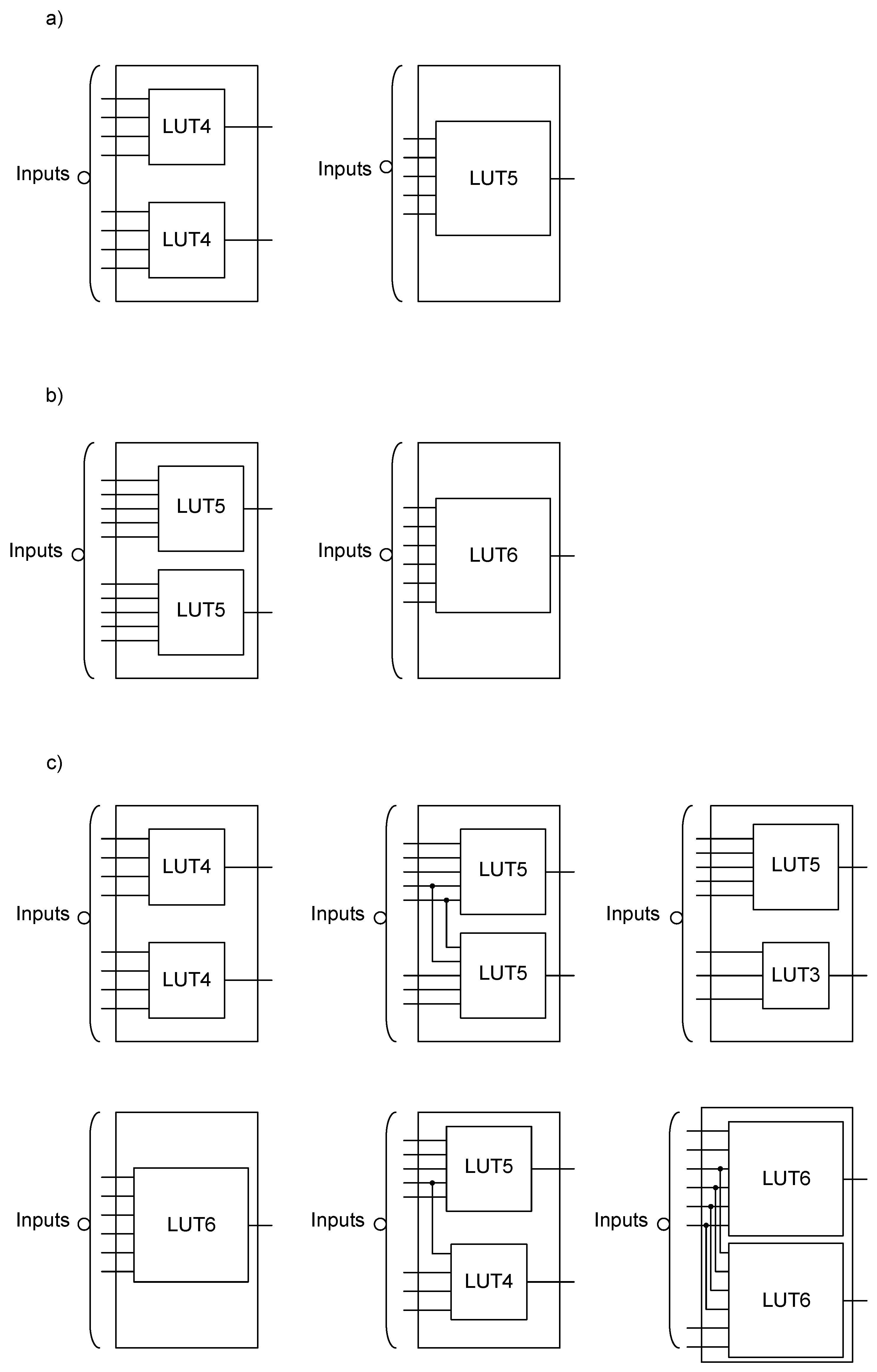
Figure 14.
Limitation of the number of LUT blocks.


Table 1.
Results of experiments (ABC, number of states <10).
| Separate Implementation | Shared Implementation | Separate im.- Shared im. | ||||||||||
|---|---|---|---|---|---|---|---|---|---|---|---|---|
| Benchmarks | δ | λ | δ + λ | |||||||||
| Name | In | Out | p | States | Blocks | Levels | Blocks | Levels | Blocks | Levels | Blocks | Levels |
| Bbtas | 2 | 2 | 24 | 6 | 4 | 2 | 2 | 1 | 6 | 2 | 0 | 0 |
| Beecount | 3 | 4 | 28 | 7 | 10 | 3 | 12 | 2 | 22 | 3 | 0 | 0 |
| dk14 | 3 | 5 | 56 | 7 | 20 | 3 | 20 | 3 | 39 | 3 | 1 | 0 |
| dk15 | 3 | 5 | 32 | 4 | 6 | 2 | 14 | 2 | 20 | 3 | 0 | −1 |
| dk17 | 2 | 3 | 32 | 8 | 33 | 4 | 22 | 4 | 54 | 4 | 1 | 0 |
| dk27 | 1 | 2 | 14 | 7 | 3 | 1 | 2 | 1 | 5 | 1 | 0 | 0 |
| ex5 | 2 | 2 | 32 | 9 | 14 | 3 | 3 | 2 | 18 | 3 | −1 | 0 |
| ex6 | 5 | 8 | 34 | 8 | 24 | 3 | 40 | 4 | 57 | 4 | 7 | 0 |
| Lion | 2 | 1 | 11 | 4 | 2 | 1 | 1 | 1 | 3 | 1 | 0 | 0 |
| lion9 | 2 | 1 | 25 | 9 | 15 | 3 | 5 | 3 | 18 | 3 | 2 | 0 |
| Mc | 3 | 5 | 10 | 4 | 3 | 2 | 4 | 2 | 6 | 2 | 1 | 0 |
| s8 | 4 | 1 | 20 | 5 | 21 | 3 | 2 | 2 | 23 | 3 | 0 | 0 |
| s27 | 4 | 1 | 34 | 6 | 5 | 2 | 2 | 2 | 6 | 2 | 1 | 0 |
| Shiftreg | 1 | 1 | 16 | 8 | 3 | 1 | 1 | 1 | 4 | 1 | 0 | 0 |
| Tav | 4 | 4 | 49 | 4 | 1 | 1 | 7 | 2 | 8 | 2 | 0 | 0 |
| train4 | 2 | 1 | 14 | 4 | 2 | 1 | 1 | 1 | 3 | 1 | 0 | 0 |
| 166 | 138 | 292 | ||||||||||
| Sum: | 304 | 292 | ||||||||||
Table 2.
Results of experiments (ABC, number of states ≥10).
| Separate Implementation | Shared Implementation | Separate im.- Shared im. | ||||||||||
|---|---|---|---|---|---|---|---|---|---|---|---|---|
| Benchmarks | δ | λ | δ + λ | |||||||||
| Name | In | Out | p | States | Blocks | Levels | Blocks | Levels | Blocks | Levels | Blocks | Levels |
| Bbara | 4 | 2 | 60 | 10 | 26 | 3 | 5 | 2 | 30 | 3 | 1 | 0 |
| Bbsse | 7 | 7 | 56 | 16 | 40 | 4 | 23 | 3 | 61 | 4 | 2 | 0 |
| dk512 | 1 | 3 | 30 | 15 | 11 | 2 | 5 | 2 | 16 | 2 | 0 | 0 |
| Donfile | 2 | 1 | 96 | 24 | 30 | 4 | 1 | 1 | 31 | 4 | 0 | 0 |
| ex2 | 2 | 2 | 72 | 19 | 45 | 4 | 9 | 3 | 56 | 4 | −2 | 0 |
| ex3 | 2 | 2 | 36 | 10 | 19 | 3 | 7 | 3 | 26 | 3 | 0 | 0 |
| ex4 | 6 | 9 | 21 | 14 | 16 | 3 | 16 | 2 | 34 | 3 | −2 | 0 |
| ex7 | 2 | 2 | 36 | 10 | 18 | 3 | 5 | 3 | 24 | 3 | −1 | 0 |
| Keyb | 7 | 2 | 170 | 19 | 87 | 6 | 13 | 4 | 105 | 5 | −5 | 1 |
| Opus | 5 | 6 | 22 | 10 | 22 | 4 | 22 | 3 | 38 | 4 | 6 | 0 |
| Sse | 7 | 7 | 56 | 16 | 36 | 4 | 28 | 3 | 59 | 4 | 5 | 0 |
| Tbk | 6 | 3 | 1569 | 32 | 122 | 6 | 22 | 4 | 136 | 6 | 8 | 0 |
| Tma | 7 | 6 | 42 | 20 | 62 | 5 | 47 | 4 | 108 | 5 | 1 | 0 |
| train11 | 2 | 1 | 25 | 11 | 14 | 3 | 7 | 3 | 21 | 3 | 0 | 0 |
| 548 | 210 | 745 | ||||||||||
| Sum: | 758 | 745 | ||||||||||
Table 3.
Results of experiments (DECOMP, number of states <10).
| Separate Implementation | Shared Implementation | Separate im.- Shared im. | ||||||||||
|---|---|---|---|---|---|---|---|---|---|---|---|---|
| Benchmarks | δ | λ | δ + λ | |||||||||
| Name | In | Out | P | States | Blocks | Levels | Blocks | Levels | Blocks | Levels | Blocks | Levels |
| Bbtas | 2 | 2 | 24 | 6 | 2.5 | 2 | 2 | 1 | 4 | 2 | 0.5 | 0 |
| Beecount | 3 | 4 | 28 | 7 | 4 | 2 | 5 | 2 | 11 | 2 | −2 | 0 |
| dk14 | 3 | 5 | 56 | 7 | 7 | 2 | 12 | 2 | 16 | 2 | 3 | −1 |
| dk15 | 3 | 5 | 32 | 4 | 2 | 1 | 5 | 1 | 7 | 1 | 0 | 0 |
| dk17 | 2 | 3 | 32 | 8 | 18 | 3 | 10.5 | 3 | 21 | 4 | 7.5 | −1 |
| dk27 | 1 | 2 | 14 | 7 | 1.5 | 1 | 1 | 1 | 2.5 | 1 | 0 | 0 |
| ex5 | 2 | 2 | 32 | 9 | 8 | 2 | 2 | 2 | 10 | 2 | 0 | 0 |
| ex6 | 5 | 8 | 34 | 8 | 8 | 4 | 18 | 4 | 20 | 4 | 6 | 0 |
| lion | 2 | 1 | 11 | 4 | 1 | 1 | 0.5 | 1 | 1.5 | 1 | 0.5 | 0 |
| lion9 | 2 | 1 | 25 | 9 | 5.5 | 2 | 1.5 | 2 | 9 | 2 | −2 | 0 |
| mc | 3 | 5 | 10 | 4 | 1.5 | 1 | 3 | 1 | 4.5 | 1 | 1 | 0 |
| s8 | 4 | 1 | 20 | 5 | 6 | 2 | 1 | 2 | 7 | 3 | 0 | −1 |
| s27 | 4 | 1 | 34 | 6 | 4 | 2 | 1 | 2 | 5 | 2 | 0 | 0 |
| shiftreg | 1 | 1 | 16 | 8 | 1.5 | 1 | 0.5 | 1 | 2 | 1 | 0 | 0 |
| tav | 4 | 4 | 49 | 4 | 1 | 1 | 5.5 | 2 | 6 | 2 | 0.5 | 0 |
| train4 | 2 | 1 | 14 | 4 | 1 | 1 | 0.5 | 1 | 1.5 | 1 | 0 | 0 |
| 72.5 | 69 | 128 | ||||||||||
| Sum: | 141.5 | 128 | ||||||||||
Table 4.
Results of experiments (DECOMP, N = number of states ≥10).
| Separate Implementation | Shared Implementation | Separate im.- Shared im. | ||||||||||
|---|---|---|---|---|---|---|---|---|---|---|---|---|
| Benchmarks | δ | λ | δ + λ | |||||||||
| Name | In | Out | P | States | Blocks | Levels | Blocks | Levels | Blocks | Levels | Blocks | Levels |
| bbara | 4 | 2 | 60 | 10 | 9 | 3 | 3 | 2 | 11 | 3 | 1 | 0 |
| bbsse | 7 | 7 | 56 | 16 | 26.5 | 4 | 23 | 5 | 37 | 4 | 2.5 | 1 |
| dk512 | 1 | 3 | 30 | 15 | 4 | 1 | 2.5 | 1 | 6.5 | 1 | 0 | 0 |
| donfile | 2 | 1 | 96 | 24 | 11 | 2 | 0.5 | 1 | 11.5 | 2 | 0 | 0 |
| ex2 | 2 | 2 | 72 | 19 | 19 | 3 | 2 | 2 | 21 | 3 | 0 | 0 |
| ex3 | 2 | 2 | 36 | 10 | 8 | 2 | 1 | 1 | 9 | 2 | 0 | 0 |
| ex4 | 6 | 9 | 21 | 14 | 7.5 | 3 | 7.5 | 2 | 21.5 | 4 | −6.5 | −1 |
| ex7 | 2 | 2 | 36 | 10 | 8 | 2 | 3 | 2 | 10 | 2 | 1 | 0 |
| keyb | 7 | 2 | 170 | 19 | 57 | 7 | 5 | 3 | 56 | 6 | 6 | 1 |
| opus | 5 | 6 | 22 | 10 | 12.5 | 3 | 12 | 3 | 22 | 4 | 2.5 | −1 |
| Sse | 7 | 7 | 56 | 16 | 25.5 | 5 | 23 | 5 | 43 | 5 | 5.5 | 0 |
| tbk | 6 | 3 | 1569 | 32 | 44 | 7 | 12 | 4 | 45 | 6 | 11 | 1 |
| tma | 7 | 6 | 42 | 20 | 37.5 | 7 | 25.5 | 7 | 61.5 | 6 | 1.5 | 1 |
| train11 | 2 | 1 | 25 | 11 | 8 | 2 | 2.5 | 2 | 9 | 2 | 1.5 | 0 |
| 277.5 | 122.5 | 364 | ||||||||||
| Sum: | 400 | 364 | ||||||||||
Table 5.
Results of experiments (Vivado and Quartus II, number of states <10).
| Vivado (Artix 7) | Quartus (Cyclone 10) | |||||||||||
|---|---|---|---|---|---|---|---|---|---|---|---|---|
| Benchmarks | Separate implem. | Shared implem. | sep.- sha. | Separate implem. | Shared implem. | sep.-sha. | ||||||
| Name | In | Out | P | States | δ | Λ | δ+λ | δ | λ | δ + λ | ||
| bbtas | 2 | 2 | 24 | 6 | 2 | 1 | 3 | 0 | 2 | 1 | 3 | 0 |
| beecount | 3 | 4 | 28 | 7 | 3 | 4 | 7 | 0 | 3 | 3 | 6 | 0 |
| dk14 | 3 | 5 | 56 | 7 | 3 | 5 | 8 | 0 | 3 | 5 | 14 | −6 |
| dk15 | 3 | 5 | 32 | 4 | 1 | 3 | 4 | 0 | 1 | 3 | 4 | 0 |
| dk17 | 2 | 3 | 32 | 8 | 14 | 10 | 24 | 0 | 11 | 7 | 18 | 0 |
| dk27 | 1 | 2 | 14 | 7 | 2 | 1 | 3 | 0 | 2 | 1 | 3 | 0 |
| ex5 | 2 | 2 | 32 | 9 | 4 | 1 | 5 | 0 | 4 | 1 | 5 | 0 |
| ex6 | 5 | 8 | 34 | 8 | 8 | 16 | 22 | 2 | 7 | 14 | 20 | 1 |
| lion | 2 | 1 | 11 | 4 | 1 | 1 | 2 | 0 | 1 | 1 | 2 | 0 |
| lion9 | 2 | 1 | 25 | 9 | 4 | 1 | 5 | 0 | 4 | 1 | 5 | 0 |
| mc | 3 | 5 | 10 | 4 | 1 | 2 | 3 | 0 | 1 | 2 | 3 | 0 |
| s8 | 4 | 1 | 20 | 5 | 6 | 2 | 8 | 0 | 7 | 1 | 9 | −1 |
| s27 | 4 | 1 | 34 | 6 | 3 | 1 | 4 | 0 | 3 | 1 | 4 | 0 |
| shiftreg | 1 | 1 | 16 | 8 | 2 | 1 | 2 | 1 | 2 | 1 | 2 | 1 |
| tav | 4 | 4 | 49 | 4 | 1 | 4 | 5 | 0 | 1 | 2 | 3 | 0 |
| train4 | 2 | 1 | 14 | 4 | 1 | 1 | 2 | 0 | 1 | 1 | 2 | 0 |
| 56 | 54 | 107 | 53 | 45 | 103 | |||||||
| Sum: | 110 | 107 | 98 | 103 | ||||||||
Table 6.
Results of experiments (Vivado and Quartus II, number of states ≥10).
| Vivado (Artix 7) | Quartus(Cyclone 10) | |||||||||||
|---|---|---|---|---|---|---|---|---|---|---|---|---|
| Benchmarks | Separate implem. | Shared implem. | sep.-sha. | Separate implem. | Shared implem. | sep.-sha. | ||||||
| Name | In | Out | P | States | δ | Λ | Δ + λ | δ | Λ | δ + λ | ||
| bbara | 4 | 2 | 60 | 10 | 9 | 3 | 13 | −1 | 11 | 2 | 15 | −2 |
| bbsse | 7 | 7 | 56 | 16 | 14 | 14 | 25 | 3 | 17 | 11 | 24 | 3 |
| dk512 | 1 | 3 | 30 | 15 | 2 | 2 | 4 | 0 | 2 | 2 | 4 | 0 |
| donfile | 2 | 1 | 96 | 24 | 5 | 1 | 6 | 0 | 6 | 1 | 6 | 1 |
| ex2 | 2 | 2 | 72 | 19 | 10 | 2 | 12 | 0 | 12 | 3 | 14 | 1 |
| ex3 | 2 | 2 | 36 | 10 | 4 | 2 | 6 | 0 | 4 | 2 | 6 | 0 |
| ex4 | 6 | 9 | 21 | 14 | 6 | 8 | 17 | −3 | 7 | 8 | 13 | 2 |
| ex7 | 2 | 2 | 36 | 10 | 4 | 1 | 5 | 0 | 4 | 1 | 5 | 0 |
| keyb | 7 | 2 | 170 | 19 | 38 | 7 | 43 | 2 | 41 | 5 | 42 | 4 |
| opus | 5 | 6 | 22 | 10 | 10 | 10 | 17 | 3 | 9 | 9 | 15 | 3 |
| sse | 7 | 7 | 56 | 16 | 16 | 13 | 27 | 1 | 16 | 11 | 26 | 1 |
| tbk | 6 | 3 | 1569 | 32 | 36 | 9 | 43 | 2 | 27 | 7 | 49 | −15 |
| tma | 7 | 6 | 42 | 20 | 23 | 17 | 44 | 2 | 25 | 16 | 40 | 1 |
| train11 | 2 | 1 | 25 | 11 | 4 | 1 | 5 | 0 | 4 | 1 | 5 | 0 |
| 181 | 90 | 267 | 185 | 79 | 264 | |||||||
| Sum: | 271 | 267 | 264 | 264 | ||||||||
© 2020 by the authors. Licensee MDPI, Basel, Switzerland. This article is an open access article distributed under the terms and conditions of the Creative Commons Attribution (CC BY) license (http://creativecommons.org/licenses/by/4.0/).
Share and Cite
MDPI and ACS Style
Kubica, M.; Kania, D. Technology Mapping of FSM Oriented to LUT-Based FPGA. Appl. Sci. 2020, 10, 3926. https://doi.org/10.3390/app10113926
AMA Style
Kubica M, Kania D. Technology Mapping of FSM Oriented to LUT-Based FPGA. Applied Sciences. 2020; 10(11):3926. https://doi.org/10.3390/app10113926
Chicago/Turabian StyleKubica, Marcin, and Dariusz Kania. 2020. "Technology Mapping of FSM Oriented to LUT-Based FPGA" Applied Sciences 10, no. 11: 3926. https://doi.org/10.3390/app10113926
Note that from the first issue of 2016, this journal uses article numbers instead of page numbers. See further details here.