Article

Numerical Study of a Polarization Selective Visual Optical Switch

Center of Material Science, National University of Defense Technology, Changsha 410073, China
*
Author to whom correspondence should be addressed.
Appl. Sci. 2020, 10(15), 5246; https://doi.org/10.3390/app10155246
Submission received: 16 June 2020 / Revised: 22 July 2020 / Accepted: 27 July 2020 / Published: 30 July 2020
(This article belongs to the Section Optics and Lasers)

Abstract

:
The subwavelength structure based on metamaterial has been widely used in the application of structure color due to its unique characteristics. Here, a composite structure consisting of a circular hole and different number of metal strips is proposed. By changing the polarization direction of the incident light, the resonance peak in the visible light range shifts, and the material presents different colors. At the same time, take advantage of the shift of the resonance peak, a plasmonic optical switch, of which on/off states can be indicated by the structural color, is constructed, and the maximum contrast ratio is more than 20 dB. In addition, by means of changing the geometric parameters and materials of the metal strip, the colors presented basically cover the whole visible light range. This method theoretically proves the feasibility of using subwavelength structure to construct visual plasmonic optical switch using structural color in the visible light range, which provides a broad prospect for the application of multiple physical mechanism in nanostructure design.

1. Introduction

Surface plasmons (SPs), as the carrier of optical information, has become a pivotal bridge between the micro-nano circuits and optical devices. SPs include surface plasmon polaritons (SPPs) and local surface plasmon polaritons (LSPs), which are surface electromagnetic waves formed by collective oscillation of free electrons interacting with incident light field in metal [1,2,3,4]. In recent years, the enhanced optical transmission (EOT) effect brought by metal-based surface plasmons has been applied in different wavelengths, including visible light, near-infrared, and infrared ranges. In particular, when the response range of electromagnetic wave is in the visible light band, the diffraction, scattering and absorption of plasmonic structures can provide us extremely vivid information, especially in color. In general, when the geometric parameters of the micro-nano structure and the types of material change, the peaks of surface plasmon resonances will change (including the position, intensity, and splitting), making the materials present different colors, namely, structural colors.
Based on the SPs, a large number of optical devices have been constructed, and its optical response can be designed by controlling the size, pattern and composition of the subwavelength units. For example, it is numerically found that the polarization state is a sensitive parameter in plasmonic EOT only when the gap size between triangular nanoapertures is less than 20 nm [5]. Through the construction of bullseye [6] and hoof-shaped [7] structures, the subwavelength metal structure has high transmittance and application prospect in enhancing optical transmission effect. Besides, these characteristics of the SPs have major applications [8,9,10] in ultra-high resolution imaging [11,12,13], inverse design [14], complementary metal oxide semiconducto (CMOS) digital integrated circuit [15,16,17], light emitting diode [18], steganography [19], and many other fields. Among of them, plasmonic optical switch (POS) plays a vital role in the construction of nanophotoniccircuits [7,10]. In particular, as a basic logic element in photoelectric data processing, the advantages of small size and fast response of the POS can make it play an important role. For example, a multi-band multi-functional photonic device, in our previous work [7], has been proposed. By changing the polarization direction of the incident light, the plasmonic splitter and switch were both constructed at different wavelengths in the near infrared range. On the other hand, due to the local field enhancement effect of the SP excited by the oscillation between the photon and electron, it can break through the diffraction limit and greatly improve the color resolution [20]. At the same time, the EOT effect brought by surface plasmon can make the structure obtain higher transmittance, leading to the stronger color display. Up to now, plasmonic structural color has drawn more attention and various applications have been proposed [21,22,23]. For example, a structure combining silicon material and refractive index matching layer is proposed to improve the color richness and brightness [24]. However, the combination of surface plasmon devices and structural colors has not been studied in depth. Based on our previous work [7], when the working state of the optical switch can be directly represented by different colors, the device can be more operable and visual.
In this paper, we present a composite structure based on filling different number of metal strips in the hollow circular holes. By rotating the polarization direction of the electric field of the incident light, the transmission peak within the visible light range shifts, and the material shows different colors. In addition, a plasmonic visual optical switch is constructed in the visible light range to directly characterize its working state by color, taking advantage of the phenomenon of displacement of transmission peak. Simultaneously, the contrast ratio of the device is more than 20 dB. Compared with the general optical switch, it can play a good role in photoelectric data processing due to its advantages of sub wavelength size and fast response. At the same time, compared with our previous work [7], the switch ratio is increased by nearly 6 dB. Finally, we change the geometric parameters (including length and width) and material types of the metal strip, so that the device has more colors and can achieve productive performance in different scenes.

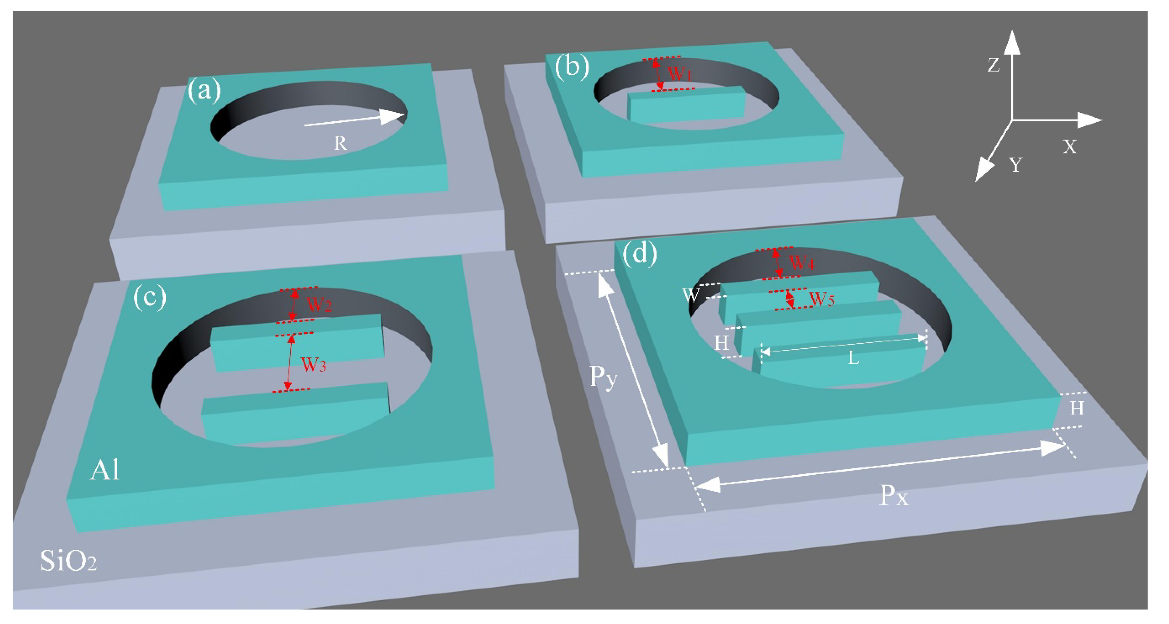
2. Design and Modeling

Figure 1 is a unit cross-sectional diagram, where the gray part is SiO2 and the blue part is aluminum (Al). Px and Py present the array periods along X- and Y-axes, respectively. The Al film thickness is 50 nm, which is placed on a quartz substrate with a thickness of 100 nm. Among them, a hollow circular hole is arranged on the metal Al film through the entire thickness of the Al film. In the hollow circular hole, we place metal strips symmetrically along the center, with the number of 1, 2, and 3, respectively. The incident light incidents vertically from one side of the quartz substrate to the surface of the metallic film in the Z direction with the electric field in the X direction. By changing the polarization direction of the electric field, the metal strip plays a different role in the surface plasmon resonance mode. The propagation process of light in periodic subwavelength metallic holes have been simulated by using the finite difference time domain (FDTD). The EOT effect of subwavelength hole arrays in metal film can be characterized by the transmittance T as following [25]: T = Pout(λ)/Pin(λ), where Pin(out) is power flux through the metal film.

3. Results and Discussions

Here, we discuss the influences of the number of metal strips, geometric parameters, and the material of strips on the EOT and the device performance.

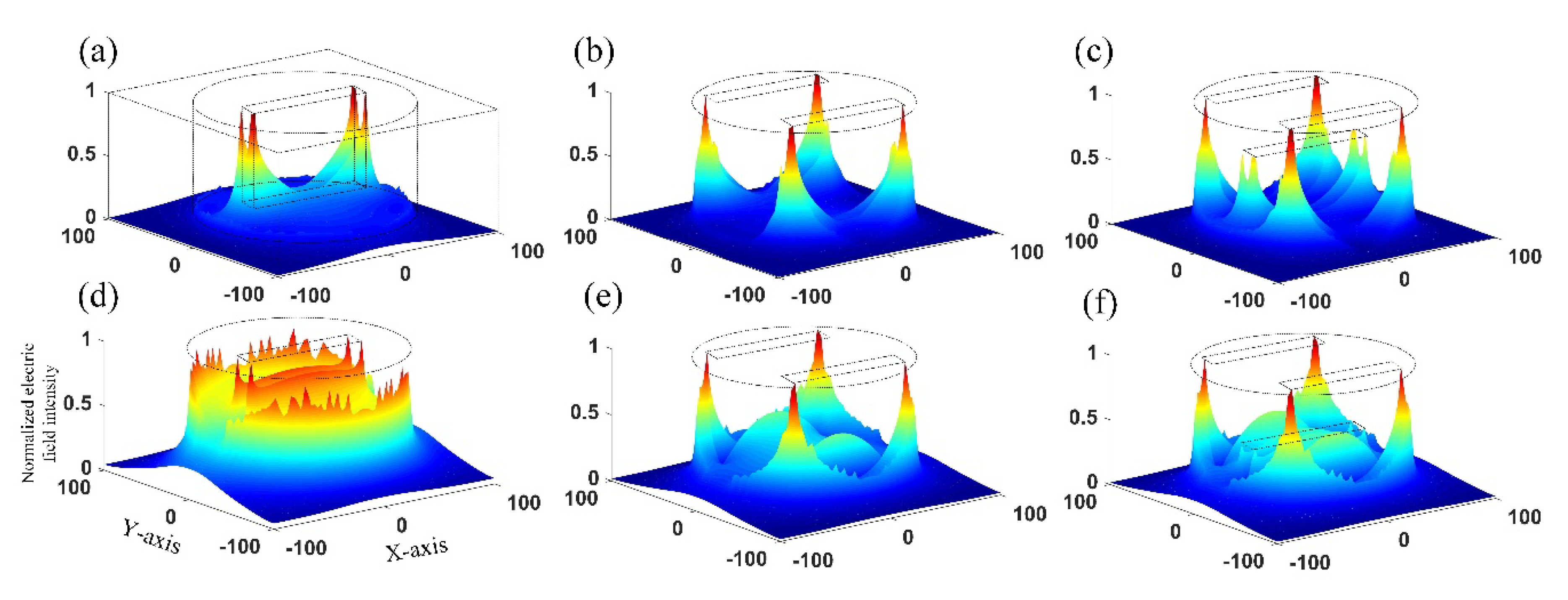
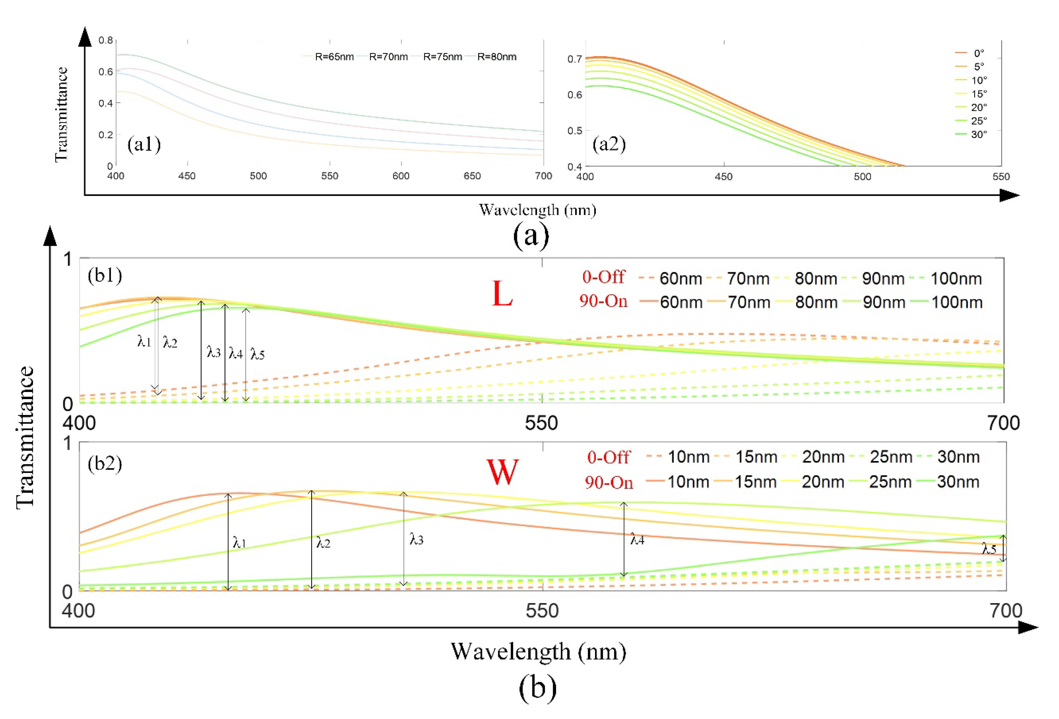
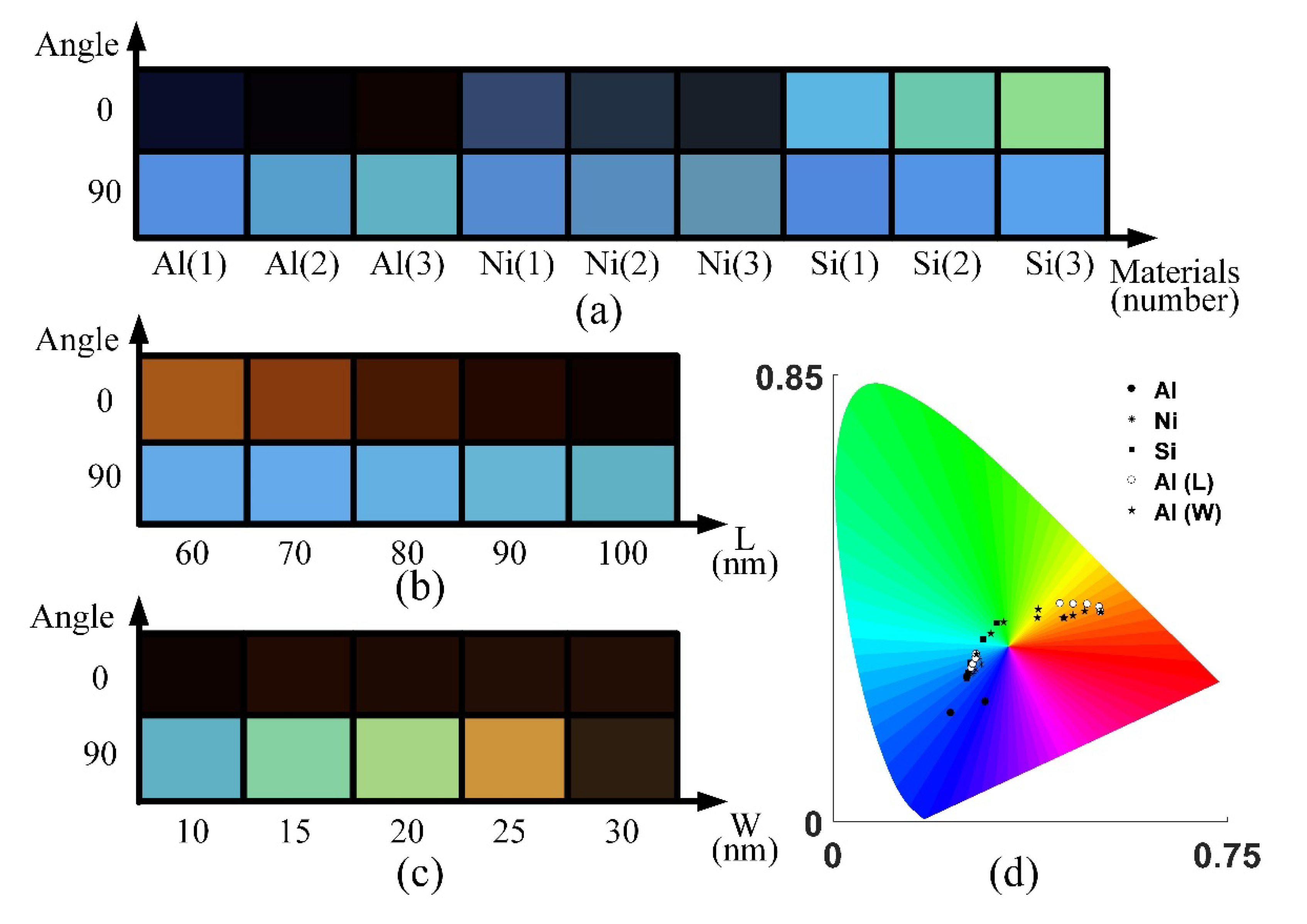
3.1. The Influence of the Number of Metal Strips on the Enhanced Optical Transmission

Considering the special function of the metal strip in the polarization direction of the incident light, a composite structure of the metal strip and the hollow circular hole is constructed. As shown in Figure 2a, the polarization direction of the electric field of the incident light is changed when there is no metal strip in the hollow circular hole, and the transmittance remain stable. Generally speaking, the resonance mode in the circular hole is mainly the SPPs resonance mode, and the primary factor affecting the transmission peak shift is the period P of the structure [26]. In addition, due to the special symmetry of the circular hole, the polarization direction of the incident light has no effect on the structure. As shown in Figure 2b–d, different number of metal strips are added to the hollow circular hole. When the polarization direction of the incident light changes from parallel to perpendicular to the X-axis, the results show that the transmission peak shifts obviously. So far, in order to unrestricted display the color rendering effect of materials, we invert the transmission spectrum of FDTD simulation into CIE1931 color coordinate map, and calculate the color coordinate points on an excellent space map [27]:
X = k λ T ( λ ) I ( λ ) x ( λ )
Y = k λ T ( λ ) I ( λ ) y ( λ )
Z = k λ T ( λ ) I ( λ ) z ( λ )
k = 100 / λ I ( λ ) z ( λ )
x = X/(X + Y + Z)
y = Y/(X + Y + Z)
where the T(λ) is the transmission spectrum we detected; I(λ) is the spectrum of the incident light source (D65); And x′(λ), y′(λ), z’(λ) represent the tristimulus value. The wavelength ranges are 400 nm to 700 nm, which basically covers the visible light ranges. And (x, y) obtained from Equations (5) and (6) is the chromaticity coordinates of the transmission spectrum. As shown in the illustration in Figure 2b–d, materials under different conditions present different colors. As shown in the figure, by changing the number of metal strips in the hollow circular hole, the different colors in the visible light range can be obtained. In addition, it is found that when the polarization direction of the incident electric field is 0° and 90°, there is a huge difference in the transmittance at a specific wavelength. This is exactly how the POS works. In other words, by rotating the polarization direction of the electric field of the incident light, the metal strip can be controlled to participate in resonance mode, thus the incident light can be turned on and off. Furthermore, when the resonance mode changes in the structure, the transmission peak of the visible light band shifts, which leads to the color change of the material surface. Take advantage of this point, we can construct a visual POS, that is to use the color change to directly characterize the different working states of the switch. Moreover, we consider that the center wavelength of the transmission peak is the working wavelength of the POS, and the performance index of the contrast ratio is used to quantitatively describe the control effect of the POS on the lamp [28]:
η = 10 log 10 ( T o n T o f f )
where Ton/off is the transmission peak at the working wavelength of the switch when the switch is on/off. As shown in Figure 2b–d, when the number of metal strips is 1, 2, and 3, the contrast ratio is 8 dB, 13.8 dB, and 20.3 dB, respectively. This is 6 dB higher than our previous work. More obviously, the different working states of the switch are directly represented by the color presentation [7]. It should be noted that when the number of metal strips is changed, the working wavelength of POS also shifts. This means that once the device is made, its working wavelength will be determined. However, in practical application, we combine the background color of the environment to select the geometric parameters of the device, so that the color produced by POS is not affected by the background color.
Here, we give the relative electric field intensity distribution diagrams under the case of different number of metal strips. As shown in Figure 3a–c, when the polarization direction of the relative electric field is parallel to the X-axis, the charge is mainly concentrated at the sharp angle of the metal strip. This is due to the fact that the spine of the structure is dominated by the LSP resonance mode. When the polarization direction of the relative electric field is perpendicular to the X-axis, the results show that in addition to a large number of charges accumulated at the sharp corner of the metal strip, there are also a large number of charges between the metal strip and the metal strip in Figure 3d–f. It can be seen from the relative electric field distribution diagrams that when the polarization direction is perpendicular to the metal strip, the space between different metal strips is equivalent to a Fabry Perot (FP) cavity. Therefore, when the polarization direction is rotated from parallel to perpendicular to the X-axis, due to the existence of the FP cavity, the resonance modes excited by the metal strip interact with each other, resulting in the shift of the transmission peak. In other words, the change of polarization direction change the coupling degree between the metal strips in the FP cavity, resulting in the shift of transmission peak [7].

3.2. The Influence of the Changing between the Different Geometric Parts of the Structure on the Enhanced Optical Transmission

In order to further explore the influence of the interaction between different geometric parts of the structure on the EOT, we firstly study the structure of hollow circular hole. As shown in Figure 4(a1), we change the radius R of a hollow circular hole. It is found that the amplitude of the transmission peak decreases slightly with the decrease of the area of the hollow circular hole. Obviously, the decrease of the area of the circular hole leads to the decrease of the incident light participating in the resonant mode. In addition, we also studied the angle between the incident light and the normal direction of the material surface. As shown in Figure 4(a2), the results are more obvious when the included angles is 0, 5, 10, 15, 20, 25, and 30 degrees respectively. The only change is the transmittance, which has no effect on the position of the transmission peak. In a single circular hole structure, the SPPs resonant mode plays a major role in EOT effect [26]. In this model, the period P of the structure is the main geometric parameter to be adjusted. In Figure 4a, the period P does not change, so the transmission peak of visible light band does not move significantly. In short, the radius of the hollow circle hole and the angle between the incident light and the normal direction of the material surface only affect the transmittance, but not the position of the transmission peak. In other words, it only affects the color saturation of the material surface, and has no obvious influence on the color types.
On the other hand, the length L and width W of the metal strip are changed when the number of the metal strip is three in Figure 4b. As shown in Figure 4(b1), when the polarization direction is parallel to or perpendicular to the X-axis, the transmission peak shows a slight red-shift as L increases from 60 nm to 100 nm. In general, when the length of the metal strip increases, the coupling degree between the metal strip and the edge of the hollow circular hole increases; at the same time, the length of the FP cavity increases, resulting in the red-shift of the transmission peak. The difference is that when the width increases, the space in the hollow circular hole decreases, which makes the effective refractive index neff in the hollow hole increase, leading to the red-shift of the transmission peak, especially when the polarization direction is 90°. Similarly, when W increases from 10 nm to 30 nm, the red-shift occurs whatever the polarization direction is 0° or 90° in Figure 4(b2).

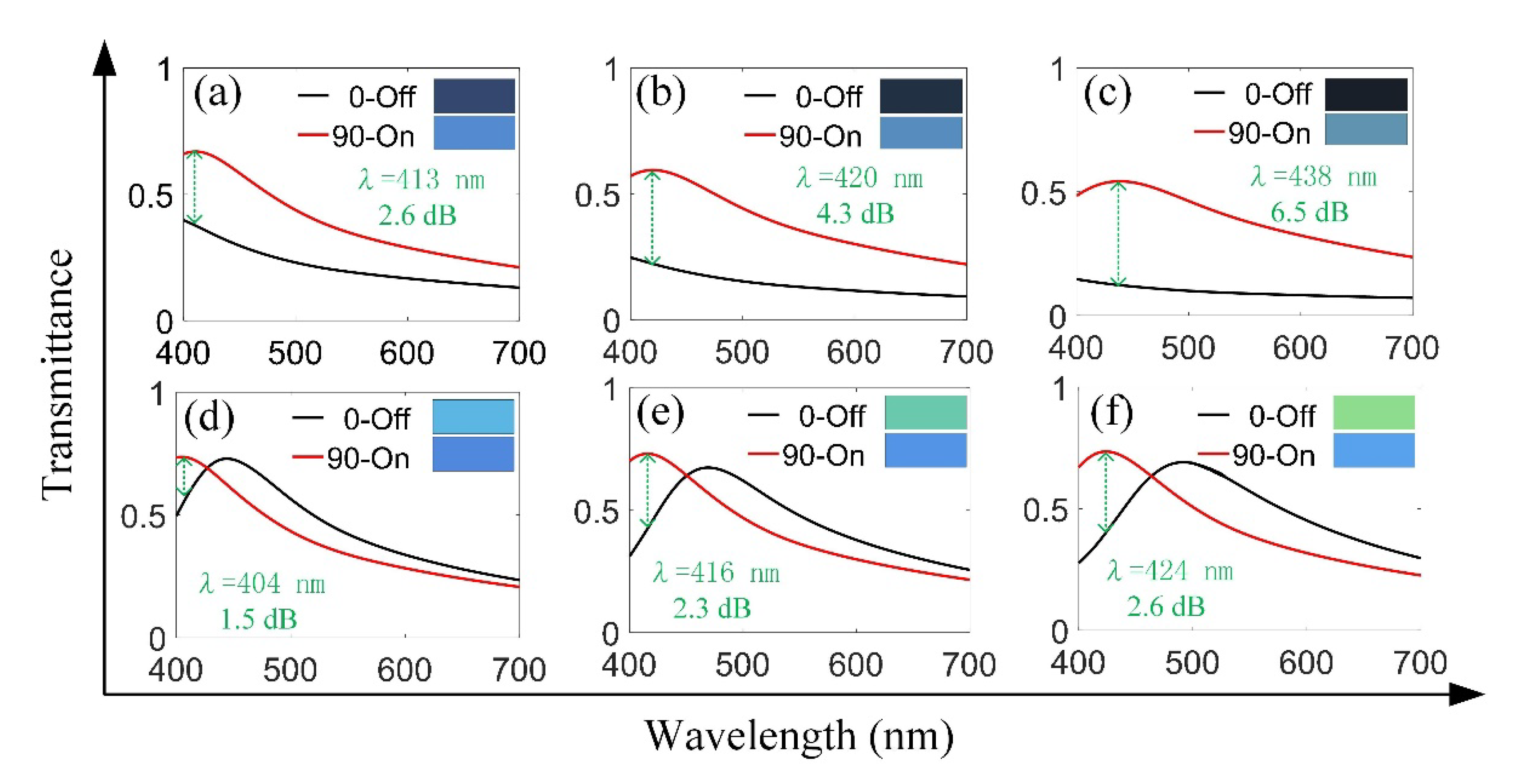
3.3. The Influence of the Changing of Metal Strip Material on the Enhanced Optical Transmission

Considering the replaceable of the metal strip, the material types of the strip are changed, including nickel (Ni) and silicon (Si). It is known from the literature that as a broadband absorption layer, ultra-thin nickel film can obtain rich structural colors with high saturation and brightness in the visible light band [29]. Silicon, as a semiconductor material, has high carrier mobility and can promote the excitation of surface plasmons [30]. Note that the geometric parameters of the structure are consistent with that of the Al material, only the material of the metal strip is changed. As shown in Figure 5a–c, the number of Ni metal strips are 1, 2, and 3, respectively. It can be seen from the figure that when the polarization direction of incident light are 0°and 90°, the colors of the material are different from that of the Al. In addition, through the calculation of Equation (7), it is found that the contrast ratio of the optical switch is relatively small. It is worth noting that when the strip material is Si in Figure 5d–f, the brightness of the color presented by the material is relatively high. It is generally known that the carrier concentration of silicon material is higher than that of the Al and Ni, resulting in higher transmittance.
In order to study its physical mechanism radically, the distributions of relative electric field intensity in X-Y plane when the strips material are Ni and Si are given. As shown in Figure 6a–f, the distributions of relative electric field intensity when the polarization direction of incident light are 0°. Obviously, the charges are basically distributed at the sharp corner of the material strip. In Figure 6(a1–f1), a large amount of electric charge are also accumulated between the material strips. There is not difference between this material strips and Al material. To date, the number of material strips, material and geometric parameters have been studied. In order to understand more intuitively the influence of these conditions on the representation of color and the size of contrast ratio, all color modules (in Figure 7a–c), as well as CIE1931 color space inversion map distribution (in Figure 7d) are given. At the same time, in Table 1 and Table 2, the contrast ratio and the working wavelength under each parameter are given.

4. Conclusions

In brief, based on a kind of composite structure with different number of metal strips in the hollow circular hole, we can adjust the position of the transmission peak within the visible range and display the corresponding color by rotating the polarization direction of the incident light. At the same time, an optical switch characterized by color, making use of the shift of transmission peak position, is constructed, and the contrast ratio of the switch is more than 20 dB. In addition, the geometric parameters (including length and width) and material strip are studied. The results show that the contrast is higher when the material strip is Al, and the color brightness is stronger when the material is Si.
Plasmonic nanostructures with resonant excitations allow the extreme confinement of incident light within nanoscale space to form an enhanced electromagnetic (EM) field. At the same time, the working state of the device can be more intuitively described by the color of the material. The combination of structure color and device provides a new method for the design of visual plasmonic device, which enriches the application of metal structure in the field of optical imaging and micro-nano devices.

Author Contributions

Conceptualization, K.W. and J.Y.; data curation, K.W.; methodology, K.W.; software, K.W., Z.Z., X.J. and J.H.; project Administration, J.Y.; supervision, J.Y.; writing—original, K.W.; writing—review, J.Y.; data analysis, K.W. All authors have read and agreed to the published version of the manuscript.

Funding

This work is supported by the National Natural Science Foundation of China (60907003, 61805278), the China Postdoctoral Science Foundation (2018M633704), the Foundation of NUDT (JC13-02-13, ZK17-03-01), the Hunan Provincial Natural Science Foundation of China (13JJ3001), and the Program for New Century Excellent Talents in University (NCET-12-0142).

Conflicts of Interest

The authors declare no conflict of interest.

References

  1. Ghaemi, H.F.; Thio, T.; Grupp, D.E.; Ebbesen, T.W.; Lezec, H.J. Surface plasmons enhance optical transmission through subwavelength holes. Phys. Rev. B 1998, 58, 6779–6782. [Google Scholar] [CrossRef] [Green Version]
  2. Barnes, W.L.; Dereux, A.; Ebbesen, T.W. Surface plasmon subwavelength Optics. Nature 2003, 424, 824–830. [Google Scholar] [CrossRef] [PubMed]
  3. Lin, L.; Roberts, A. Light transmission through nanostructured metallic films: coupling between surface waves and localized resonances. Opt. Express 2011, 19, 2626–2633. [Google Scholar] [CrossRef] [PubMed]
  4. Garcia, V.F.J.; Moreno, L.M.; Ebbesen, T.W.; Kuipers, L. Light passing through subwavelength apertures. Rev. Mod. Phys. 2010, 82, 729–787. [Google Scholar] [CrossRef] [Green Version]
  5. Jongkyoon, P.; Hyunsoo, L.; Alexander, G.; Kyujung, K.; Seungchui, K. Spectral shifting in extraordinary optical transmission by polarization-dependent surface plasmon coupling. Plasmonics 2019, 15, 489–494. [Google Scholar]
  6. Yang, Z.H.; Song, Y.; Chen, S.; Gao, Y. Control of EOT of subwavelength metal bullseye structures by coaxial nano-columns. Opto-Electron. Eng. 2018, 45, 180207–180216. [Google Scholar]
  7. Wen, K.; Zhang, Z.J.; Jiang, X.P.; He, J.; Yang, J.B. Plasmonics induced multifunction optical device via hoof-shaped subwavelength structure. Appl. Sci. 2020, 10, 2713. [Google Scholar] [CrossRef] [Green Version]
  8. Wen, K.; Jiang, X.P.; He, J.; Li, G.F.; Yang, J.B. Color-adjustable devices based on the surface plasmons effect. Appl. Sci. 2020, 10, 1960. [Google Scholar] [CrossRef] [Green Version]
  9. Zhou, H.; Zhen, B.; Hsu, C.W.; Miller, O.D.; Johnson, S.G.; Joannopoulos, J.D.; Soljacic, M. Perfect single-sided radiation and absorption without mirrors. Optica 2016, 3, 1079–1086. [Google Scholar] [CrossRef]
  10. Sun, T.M.; Deng, Z.X.; Sheng, J.B.; Chen, Z.Y.; Zhu, W.H.; Guo, W.; Wang, X.L. A compact optical switch via plasmonics of subwavelength circular-sharp hole arrays in metal films. Ann. Phys. 2017, 530, 1–6. [Google Scholar] [CrossRef]
  11. Wang, J.; Fan, Q.; Zhang, S.; Zhang, Z.; Zhang, H.; Liang, Y.; Cao, X.; Xu, T. Ultra-thin plasmonic color filters incorporating free-standing resonant membrane waveguides with high transmission efficiency. Appl. Phys. Lett. 2017, 110, 031110–031113. [Google Scholar] [CrossRef]
  12. Shu, F.; Yu, F.; Peng, R.; Zhu, Y.; Xiong, B.; Fan, R.; Wang, Z.; Liu, Y.; Wang, M. Dynamic plasmonic color generation based on phase transition of vanadium dioxide. Adv. Opt. Mater. 2018, 6. [Google Scholar] [CrossRef]
  13. Wang, B.; Dong, F.L.; Li, Q.T.; Yang, D.; Sun, C.W.; Chen, J.J.; Song, Z.W.; Xu, L.H.; Chu, W.G.; Xiao, Y.F.; et al. Visible-frequency dielectric metasurfaces for multiwavelength achromatic and highly dispersive holograms. Nano Lett. 2016, 16, 5235–5240. [Google Scholar] [CrossRef]
  14. Huang, Z.; Liu, X.; Zang, J.F. Inverse design of structural color using machine learning. Nanoscale 2019, 11, 21748–21758. [Google Scholar] [CrossRef]
  15. Guo, T.B.; Evans, J.; Wang, N.; He, S.L. Monolithic chip-scale structural color filters fabricated with simple UV lithography. Opt. Express 2019, 27, 21646–21651. [Google Scholar] [CrossRef] [PubMed]
  16. Yokogawa, S.; Burgos, S.P.; Atwater, H.A. Plasmonic color filters for CMOS image sensor applications. Nano Lett. 2012, 12, 4349–4354. [Google Scholar] [CrossRef]
  17. Yu, Y.; Chen, Q.; Wen, L.; Hu, X.; Zhang, H. Spatial optical crosstalk in CMOS image sensors integrated with plasmonic color filters. Opt. Express 2015, 23, 21994–22003. [Google Scholar] [CrossRef] [PubMed]
  18. Xin, J.Z.; Hui, K.C.; Wang, K.; Chen, H.L.W.; Ong, D.H.C.; Leung, C.W. Thermal tuning of surface plasmon resonance: Ag gratings on barium strontium titanate thin films. Appl. Phys. A 2012, 107, 101–107. [Google Scholar] [CrossRef]
  19. Zhao, R.; Sain, B.; Wei, Q.; Tang, C.; Li, X.; Weiss, T.; Huang, L.; Wang, Y.; Zentgraf, T. Multichannel vectorial holographic display and encryption. Light. Sci. Appl. 2018, 7, 95–104. [Google Scholar] [CrossRef] [PubMed] [Green Version]
  20. Al-Salem, S.M.; Lettieri, P.; Baeyens, J. Recycling and recovery routes of plastic solid waste (PSW): A review. Waste Manage. 2009, 29, 2625–2643. [Google Scholar] [CrossRef] [PubMed]
  21. Min, C.; Wang, P.; Chen, C.; Deng, Y.; Lu, Y.; Ming, H.; Ning, T.; Zhou, Y.; Yang, G. All-optical switching in subwavelength metallic grating structure containing nonlinear optical materials. Opt. Lett. 2008, 8, 869–871. [Google Scholar] [CrossRef] [PubMed]
  22. Steven, L.; Daniel, C.; Bin, A.; Yiping, Z. The extraordinary optical transmission and sensing properties of Ag/Ti composite nanohole arrays. Phys. Chem. Chem. Phys. 2019, 21, 3771–3780. [Google Scholar]
  23. Zheng, J.P.; Zhou, J.; Zeng, P.; Liu, Y.; Shen, Y.P.; Yao, W.Z.; Chen, Z.; Wu, J.H.; Xiong, S.; Chen, Y.Q.; et al. 30 GHz surface acoustic wave transducers with extremely high mass sensitivity. Appl. Phys. Lett. 2020, 116, 123502–123511. [Google Scholar] [CrossRef] [Green Version]
  24. Yang, W.H.; Xiao, S.M.; Song, Q.H.; Liu, Y.L.; Wu, Y.K.; Wang, S.; Yu, J.; Han, J.C.; Tsai, D.P. All-dielectric metasurface for high-performance structural color. Nat. Commun. 2020, 11, 1864–1872. [Google Scholar] [CrossRef] [PubMed] [Green Version]
  25. Ruan, Z.C.; Qiu, M. Enhanced transmission through periodic arrays of subwavelength holes: the role of localized waveguide resonances. Phys. Rev. Lett. 2006, 96, 233901–233904. [Google Scholar] [CrossRef]
  26. Degiron, A.; Ebbesen, T.W. The role of localized surface plasmon modes in the enhanced transmission of periodic subwavelength apertures. J. Opt. A Pure Appl. Opt. 2005, 7, S90–S96. [Google Scholar] [CrossRef]
  27. Ameri, T.; Dennler, G.; Waldauf, C.; Azimi, H.; Seemann, A.; Forberich, K.; Hauch, J.; Scharber, M.; Hinger, K.; Brabec, C.J. Fully solution-processing route toward highly transparent polymer solar cells. Adv. Funct. Mater. 2010, 20, 1592–1598. [Google Scholar] [CrossRef]
  28. Chen, F.; Yao, D.Z. Tunable multiple all-optical switch based on multi-nanoresonator-coupled waveguide systems containing Kerr material. Opt. Commun. 2014, 312, 143–147. [Google Scholar] [CrossRef]
  29. Yang, Z.M.; Chen, Y.Q.; Zhou, Y.M.; Wang, Y.S.; Dai, P.; Zhu, X.P.; Duan, H.G. Microscopic interference full-color printing using grayscale-patterned frabry-perot resonance cavities. Adv. Opt. Mater. 2017, 5, 1700029–1700038. [Google Scholar] [CrossRef]
  30. Yang, Z.M.; Zhou, Y.M.; Chen, Y.Q.; Wang, Y.S.; Dai, P.; Zhang, Z.G.; Duan, H.G. Reflective color filters and monolithic color printing based on asymmetric fabry-perot cavities using nickel as a broadbang absorber. Adv. Opt. Mater. 2016, 4, 1196–1202. [Google Scholar] [CrossRef]
Figure 1. Structural cross-sectional diagram of the unit structure in the X-Y plane. R represents the circular structure radius; H is the thickness of the Al; L and W are the length and width of the metal strip; W(1–5) are the distance between metal strips; Px and Py are the periods; As follows: H = 50 nm; L = 100 nm; W = 10 nm; Px = Py = 200 nm; W1 = 75 nm; W2 = 30 nm; W3 = 80 nm; W4 = 30 nm; W5 = 35 nm; (a) Hollow circular hole; (b) one metal strip; (c) two metal strips; (d) three metal strips; the metal strips are symmetrically distributed along the center of the circular hole.
Applsci 10 05246 g001
Figure 2. Transmittances of different polarization directions (Parallel to X-axis is 0°; Perpendicular to X-axis is 90°) under the different number of metal strips. (a) Hollow circular hole; (b) one metal strip; (c) two metal strips; (d) three metal strips. The inset is CIE1931 color space inversion map distribution.
Applsci 10 05246 g002
Figure 3. The electric field distribution diagrams in the cases of different number of metal strips. (ac) The polarization direction (0°) of the relative electric field is parallel to the X-axis; (df) The polarization direction (90°) of the relative electric field is perpendicular to the X-axis.
Applsci 10 05246 g003
Figure 4. Transmittance diagram in different situations. (a1) When there is no metal strip in the hollow hole, the radius R of the hollow hole is changed; (a2) when there is no metal strip in the hollow hole, angle between incident light and normal direction of material surface; (b1) when the number of the metal strips is three, the L changes; (b2) when the number of the metal strips is three, the W changes.
Applsci 10 05246 g004
Figure 5. (ac) Transmittances of different number of Ni metal strips; (df) Transmittances of different number of Si strips.
Applsci 10 05246 g005
Figure 6. The relative electric field distribution diagrams in the cases of different materials and the number of material strips. (ac) is Ni; (df) is Si. When there is subscript, the polarization direction is 90°.
Applsci 10 05246 g006
Figure 7. (ac) The colors of the material in different cases; (d) CIE1931 color space inversion map distribution under different conditions.
Applsci 10 05246 g007
Table 1. The contrast ratio and the working wavelength of different material strips.
AlNiSi
Number of metal strips123123123
The working wavelength (nm)411442450413420438404416424
The contrast ratio (dB)813.820.32.64.36.51.52.32.6
Table 2. The contrast ratio and the working wavelength of different geometric parameter when the metal strip number is 3.
LW
Size (nm)607080901001015202530
The working wavelength (nm)426428437446453453479502577698
The contrast ratio (dB)911.615.518.321.221.214.312.88.22.7

