1. Introduction
DC-AC inverters find widespread usage in many residential, industrial and military applications. With the ever-increasing development of the renewable energy technology, DC-AC inverters have become one of the most attractive and viable solutions to the power conversion problem. They are extensively used and play key roles in various actual applications of power electronics technologies for renewable energy sources [
1,
2,
3]. They are also used in motor drive [
4,
5] and DSTATCOM applications [
6] as well as in many uninterruptible power supply system applications such as plant facilities and factories, medical equipments and centers in hospitals, airline computer and communication systems in server farms and web hosting sites [
7]. One of the important tasks in the design of DC-AC inverters is the control loop implementation which must ensure a system free from any kind of instabilities. However, it is well known that this aim is difficult to be achieved for all values of system parameters and that many undesired nonlinear phenomena can arise in these kinds of indispensable parts of modern and emerging energy systems. These phenomena can significantly jeopardize the system performance and can cause serious consequences on its reliability.
Therefore, understanding these nonlinear phenomena, their analysis, prediction and control have increasingly become of great concern of many researchers all over the world [
8,
9,
10,
11,
12,
13,
14,
15,
16,
17,
18,
19,
20,
21,
22]. The major part of the analytical results on subharmonic oscillation in power electronics converters has been achieved for DC-DC converters [
23,
24,
25,
26,
27,
28,
29,
30,
31,
32,
33,
34,
35,
36,
37,
38,
39,
40]. DC-AC inverters are more difficult to deal with, since their dynamics is governed by two vastly different frequencies, namely the high switching frequency and the low frequency of the output voltage reference sinewave.
For reliable and desirable operation, the stability of the system must be guaranteed for the whole range of its parameters. In [
13], the dynamics behavior of an H-bridge under a digital Current Mode Control (CMC) was investigated by using a one dimensional discrete time model. Different dynamical behaviors for the system were revealed by varying the proportional gain of the current controller. In [
14] a similar approach was applied and it was demonstrated that different types of bifurcations (instabilities) can take place such as period doubling leading to Subharmonic Oscillation (SO) and border collision bifurcations leading directly to chaotic behavior.
Using the quasi-static approximation, in [
15] the slow-scale and fast-scale instabilities in a voltage-mode controlled H-bridge inverter are reported and analyzed using an averaged model and a discrete-time model respectively. It is well known that conventional averaged model cannot predict the fast-scale instability and for that the discrete-time model must be used. A closed form discrete time model was used in [
16] to predict both the slow-scale and the fast-scale instabilities in an H-bridge inverter demonstrating that the system may undergo instability phenomenon when the proportional gain of the voltage controller is increased. In an H-bridge digital-controlled grid-connected inverter system, bifurcation behavior was investigated and loss of system stability was shown by increasing the current controller gain [
19] and it was shown that in this system only slow scale instability may take place leading to low-frequency oscillation. The same system, but with double edge modulation, has been studied in [
9] using an analytical closed-form expression for predicting a period doubling phenomenon.
Single-stage grid-connected DC-AC conversion systems with boosting voltage capability have recently attracted the attention of many researchers. Single-stage structures of inverters not only perform DC-AC conversion but also perform voltage boosting. Moreover, differential inverter topologies seem to prevail in price and size due to the utilization of small passive elements of DC-DC converters hence improving the efficiency. In contrast to the conventional H-bridge inverter, the differential boost inverter is a flexible DC-AC inverter topology providing voltage step-up capability and could be a potential candidate for many DC-AC electrical energy conversion applications such as for power processing stage fuel-cell energy system [
41,
42], for high quality sine wave generation with a high oscillation frequency [
43], for AC-module microinverters in PV systems such as in [
44,
45,
46] among others.
In stand-alone operation mode, the load is directly supplied by the inverter. Single-phase H-bridge inverters are simple bidirectional converter topologies capable of handling both real and reactive power having their performance evaluated in terms of power quality and stability. Therefore, generating a high quality output voltage with low distortion and good voltage regulation is the main target. Other relevant performance metrics include disturbance rejection, transient response, and insensitivity to load and system parameter variations. These metrics can only be achieved with a design free from any kind of instability.
Since its introduction in [
47], many studies have dealt with the control design of the differential boost inverter using different approaches and strategies [
44,
45,
47,
48,
49]. The focus in most of the works published about this inverter is on the control design. However, the analysis of its nonlinear behavior has not been addressed in the past. Namely, SO has not been studied in this kind of inverter. Therefore the aim of this paper is to apply the Floquet theory for accurately predicting the onset of SO in a differential boost inverter. In contrast to existing works on predicting such a complex behavior in DC-AC inverters based mainly on numerical procedures, here both numerical and analytical approaches are combined to provide a comprehensive study of the systems dynamical behavior.
The prediction of this phenomenon is of high importance from both theoretical and practical points of view because it leads to an increase in the ripple of the currents and voltages and this has a harmful effect on the system performances since the overall losses become more significant. The power quality can also be jeopardized if SO is more pronounced since it can increase the THD and the current stress on the switches. Therefore, accurate modeling and stability analysis are necessary for exploring the dynamic behavior and predicting the stability boundaries of DC-AC inverters.
The remaining of this paper is organized as follows. In
Section 2, the system dealt with in this study is described. In
Section 3, the dynamic behavior of the system is explored revealing that the behavior of the system waveforms is phase-dependent. The system is shown to exhibit local instability phenomenon over a specific interval within the main sinusoidal cycle. The onset of the observed bubbling is associated to a SO phenomenon taking place at the fast switching scale. The mathematical modeling is addressed in
Section 4 in the continuous-time domain. In order to analyze the observed phenomena in
Section 3, Floquet theory is applied to the derived model in
Section 5. Thereafter, in
Section 6, the stability boundaries in terms of suitable parameters is reported. Finally, in
Section 7 the results of the study are summarized.
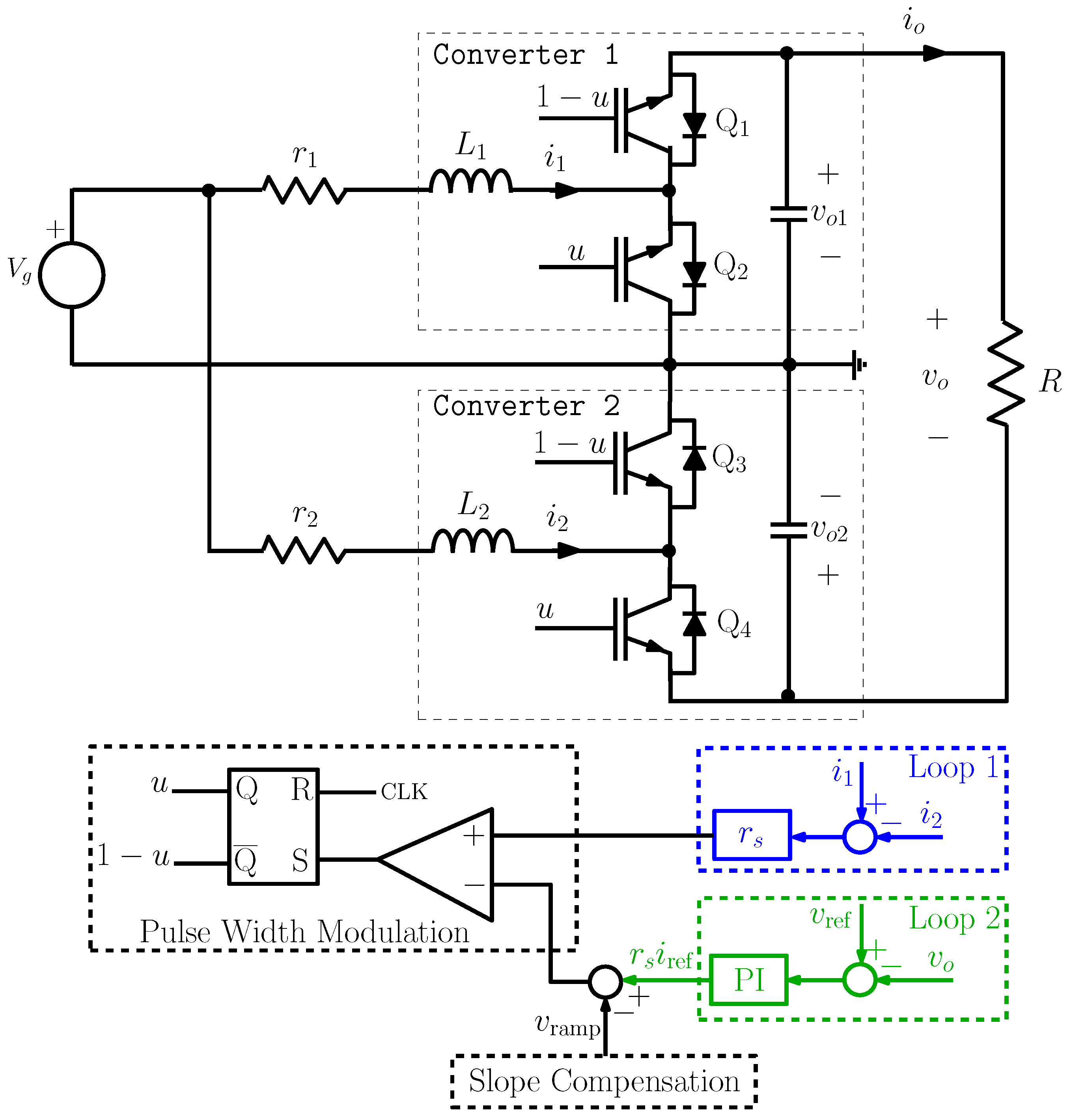
2. Differential Boost Inverter under Two-Loop Control
The system under study in this paper consists of a differential boost inverter which is obtained by connecting two identical DC-DC boost converters in parallel supplied from a common electrical energy source and feeding a floating voltage load connected between the outputs of the two converters [
47,
50]. Its schematic diagram is shown in
Figure 1. The current drawn by the input is shared properly between the two boost converters by the action of a CMC scheme using the difference between the two inductor currents, as will be detailed later. For that, two complementary control signals are considered to control the switches of the differential inverter.
Let us denote the two connected converters as
Converter 1 with inductor
and inductor current
and
Converter 2 with inductor
and inductor current
. Both converters are controlled in a complementary way using CMC via single Pulse-Width Modulation (PWM) scheme so that
Converter 2 is phase shifted
with respect to
Converter 1 at the switching time scale,
D being the operating duty cycle. Namely, the difference between
and
(scaled by a sensing resistance
) is controlled using a conventional peak CMC by comparing the signal
to the signal
. A periodic ramp signal
with amplitude
and period
T is subtracted from
for slope compensation. The comparison of the signal
with the signal
by using a comparator and a set-reset flip-flop generate the high and low values of the pulses driving the switches as shown in
Figure 1 where the block diagram of the inner current control together with the outer voltage control are depicted.
The reference current for the difference between the two inductor currents is provided by an external voltage loop. The activation of the switches Q
, Q
, Q
and Q
is carried out as follows: the signal
is connected to the non inverting pin of the comparator whereas the signal
is applied to the inverting pin. The output of the comparator is applied to the reset input of a set-reset flip-flop and a periodic clock signal is connected to its set input, as shown in
Figure 1, in such a way that the switch Q
and Q
are
on at the beginning of each switching cycle and are turned
off whenever
. The state of the switches Q
and Q
are complementary to the switches Q
and Q
respectively.
To fulfill the requirements of the underlying electronic application, a DC-AC inverter has to produce a periodic sinewave-shaped output voltage under normal operational conditions. Let
be the voltage reference that can be expressed as
, where
,
is the peak value of the output voltage reference,
its angular frequency and
its phase angle. In practical applications, the switching frequency is much higher than the AC output voltage frequency. This condition is met in this paper and it allows the use of quasi-static approximation. The error voltage
is the input signal to the voltage controller of which the task is to make the output voltage of the inverter an AC sinusoidal signal with zero DC component. Therefore, the load connected between the converters outputs will be subjected to an AC sinusoidal voltage with a zero DC component. This control strategy is different from the one used in most of the published works about this inverter topology such as [
44,
45,
47] where the control is performed such that each boost converter generates a DC bias and an AC component. In the low frequency averaged sense, the AC component of each converter is out of phase regarding the other converter. The DC component is the same for both converters.
The voltage controller is conventionally a PI regulator aiming to make the load voltage to accurately track the sinewave voltage reference . Its transfer function can be expressed as , where is its proportional gain and is its time constant.
3. Behavior of the Differential Boost Inverter
The dynamical behavior of the boost inverter is explored in this section with the aim to gain insight on suitable ways of obtaining an appropriate model that can be used for its accurate stability analysis. The system is first studied through simulations using the full-order switched model of the inverter implemented using PSIM© software by varying suitable system parameters. The focus is first on system stability in terms of the time varying voltage reference. The fixed parameter values used for the rest of the study are reported in
Table 1. Many time-domain waveforms have been computed to get a clear view of the system behavior and only representative results are shown below. The simulation is run for sufficiently long time to allow the system to reach its steady-state. The data obtained during time transient within the startup phase and during the transient regime of the regulation phase are fully eliminated. Only the last two cycles of the output voltage reference are plotted.
Figure 2 shows the system waveforms when the system is stable. The figure shows the time-domain waveforms of the reference voltage
and the output voltage
, the capacitor voltages
and
, the inductor currents
and
and the control signal
and the signal
. It is worth noting that the output voltage cannot be distinguished from its reference signal
due to the practically zero amplitude and phase errors. Note also that the state variables and the control signal oscillate at two main frequencies, the switching frequency (100 kHz) and the reference voltage frequency (50 Hz). From a practical point of view, the output voltage is characterized by a low value of THD as required in any application.
As parameters are varied, the state variables undergo a sudden distortion by exhibiting SO at the fast switching scale as shown in
Figure 3 for
. This phenomenon takes place when the proportional gain
gradually increases and reaches a critical value close to
. As shown in
Figure 3, it can be observed that the inductor currents
and
exhibit SO leading to disrupting bubbling phenomenon of the waveforms. In particular, when
, the fast-scale instability develops in all the state variables but it is more visible and pronounced in the inductor current waveforms
and
and their combination
. As stated before, such behavior manifests itself as a period-doubling phenomenon at the fast switching scale [
9,
51]. It can also be noticed in
Figure 4 that the phenomenon already becomes visible in the capacitor voltages and the output voltage hence it can deteriorate the performance of the inverter and therefore its prediction is an important task from a practical point of view.
By carefully examining the waveforms, the following statements can be made:
By increasing progressively the proportional gain and when this parameter reaches the critical value, SO oscillation starts first occurring in a very limited number of switching cycles during the first half cycle of the sinewave signal eventually in the neighborhood to the quarter of the cycle where the sinewave signal is maximum.
The number of the switching cycles, during which SO is exhibited, gets larger and the fast-scale SO is more pronounced when the proportional gain is increased.
At the left and at the right of the maximum values during the same half cycle, one has the same values of quasi-steady-state duty cycles and therefore, theoretically, a perfect symmetry is expected in the critical phase angles at which SO takes place. However, an asymmetry can take place because the slope of the reference sinewave signal at the left of the peak point is positive while it is negative at the right side.
The SO interval is repetitive from a sinewave cycle to the next one and the study of SO phenomenon can be restricted to one sinewave cycle in terms of the phase angle as a slowly varying parameter in the range .
Apparently, if SO is avoided for the first half cycle of the sinewave signal, it will also be avoided for the second half cycle. Therefore, the numerical and the analytical studies to be presented later will be restricted to the first half cycle of the sinewave signal for , i.e., only within the duty cycle range .
A powerful tool for clearly illustrating the SO phenomenon is by using the sampled waveforms. In order to clearly appreciate the change in the behavior of the system, sampled steady-state values of the state variables at time instants () are obtained. Therefore, the state variables are sampled at every clock instant and then plotted in the time domain. A priori, any one of the state variables can be used for illustrating the behavior of the system. However, as observed in the previous time domain numerical simulations, SO is more pronounced in some state variables than others. An interesting and naturally sampled variable for which SO is well noticed is the duty cycle of the binary signal u.
Figure 5 shows the waveforms of the duty cycle
(
) during one complete sinewave cycle for four different values of the proportional gain
. The duty cycle waveforms are plotted in terms of the phase angle within the interval (0,
). For
, the system exhibits a stable periodic regime in steady-state, the duty cycle does not present any disruption and its samples represent a clean and smooth waveform. When the SO regime starts taking place, one gets a different picture. For instance, for
, it can be clearly seen that there is a certain phase interval within the first half of the sinewave cycle during which the duty cycle waveforms is disrupted. Namely, within the phase interval defined by two critical phase angles, two different branches of duty cycle values appear instead of one a kind of bubble emerges [
18]. It can be observed that the onset of bubbling phenomenon depicted in
Figure 5 is gradual. First, for a relatively small value of the parameter
, the cycle is smooth, then, for increasing
, it becomes disrupted in a small phase interval. Thereafter, as
is further increased, the interval
of
during which SO takes place grows up as can be seen in
Figure 5. If the proportional gain is further increased, this interval gets wider and the phenomenon usually spreads through the whole line cycle.
Figure 5 also shows that successive period doubling inside the SO interval may also take place in the first half cycle where the voltage reference is positive, i.e., when
. When
becomes even larger, the bubbles start appearing even in the second half cycle of voltage reference where
. Therefore, even for
, the voltage loop may have a destabilizing effect since when the proportional gain
is increased beyond a critical value
, SO and the associated bubbling starts appearing for
and even in the presence of slope compensation. Therefore, the ramp slope needed for eliminating SO is larger than the one obtained when ignoring the effect of the voltage loop. This destabilizing effect of the voltage loop is similar to the one reported in [
27] for the buck converter and in [
24] for the boost converter. Similar behaviors have been obtained when other parameters such as the input voltage
or the inductance
L are varied.
5. Accurate Stability Analysis Using Floquet Theory
The differential equations describing the dynamics of switching converters are time periodic with the switching period
T determining the periodicity of solutions at the fast switching scale. DC-AC inverters are also time periodic with the switching period
T and the voltage reference period
. For such time periodic systems Floquet theory can be used to study the stability of periodic orbits [
53]. Here, this theory will be applied using a quasi-static approximation treating the DC-AC inverter as a DC-DC converter with a slowly varying reference voltage and duty cycle. With this approximation, the reference voltage
is considered constant within a switching cycle.
Floquet theory has been widely used in the analysis of stability of dynamical systems [
53] in general and switching converters in particular [
38,
39,
40]. For DC-DC converters, the stability dynamics at the fast switching cycle can be accurately predicted by analyzing the stability of the fixed points of the Poincaré map of the system using its Jacobian matrix or using Floquet theory combined with Filippov method which leads to the same results as the Poincaré map [
38]. The main tool for studying the stability of periodic orbits using Floquet theory is the principal fundamental matrix or the monodromy matrix
. This matrix plays a key role in the accurate stability analysis of switching systems [
38,
39,
40,
53]. The monodromy matrix is such that the dynamics in the vicinity of a quasi-static periodic orbit can be expressed as follows
where the overhat stands for small signal variations. Its eigenvalues are called the
characteristic multipliers or
Floquet multipliers and it can be seen that they determine the amount of contraction or expansion near a periodic orbit and hence they determine the stability of these periodic orbits.
Let us start by finding the monodromy matrix
. Let
the quasi-steady-state value of the state vector. Let
be the value of
at time instant
, where
,
,
,
,
,
. Let
and
be the vector fields for
and
respectively. Let us define the augmented state vector
. Let
,
,
,
,
and
be, respectively, the associated augmented state matrices, input vectors, vector of external parameters and vector of feedback coefficients that are expressed as follows
Let us also define the augmented state transition matrices
and
and the augmented vector fields
and
. Then, the full-order monodromy matrix can be expressed as follows [
38]
where
is the saltation matrix adapted from [
38] as follows
where
is the slope of the ramp compensator and
is the slope contributed by the time variation of the sinusoidal voltage reference. The expression of
, the third component of
, can be obtained from (
17) in steady-state which gives the following expression for
Now that the expression of the monodromy matrix was derived, hereinafter, we will pay special attention to the movement of the Floquet multipliers as the voltage reference varies quasi-statically. This is equivalent to changing the phase angle or the quasi-steady-state duty cycle D. We will also study the movement of the Floquet multipliers when the proportional gain of the controller or the amplitude of the ramp compensator are varied. Any crossing from the interior of the unit circle to its exterior indicates a lost of stability of the desired orbit. The system becomes unstable, if at least one root of the Floquet multiplier leaves the unit circle, which is equivalent to an eigenvalue leaving the unit circle. Thus, for the stability boundary for at least one eigenvalue of holds. In particular, if a real characteristic multiplier goes through as it moves out of the unit circle, SO at the fast switching scale takes place.
To locate the boundary of SO, the Floquet multipliers are obtained. By varying the quasi-steady-state duty cycle
D, the operating point
was first calculated and the monodromy matrix was obtained for two different values of the proportional gain
. At a point where a subharmonic regime emerges, one of the eigenvalues is equal to
.
Figure 6 shows the Floquet multipliers loci in the complex plane when the quasi-steady-state duty cycle varies. The duty cycle
D was varied by varying the voltage reference between 0 and its maximum values giving rise to
. As it can be observed from
Figure 6a, for
all the eigenvalues remain inside the unit circle for the full considered range of the duty cycle. Then, the gain
was fixed at
then the reference voltage was varied in the same range as before and the results are depicted in
Figure 6b. It can be observed that one of the eigenvalues of the monodromy matrix crosses the unit circle from the point
in the complex plane indicating SO at a certain value of
very close to its maximum value. The critical value of
at which this starts taking place is
which is in a remarkable agreement with the time-domain numerical simulations presented in
Section 3.
6. Stability Boundaries in the Parameter Space
If SO boundary is of concern, the expression of the characteristic equation
can be used by imposing that an eigenvalue
and solving the resulting equation in a suitable projection of the parametric space. Therefore, to determine the boundary of SO, the following equation is solved for a certain system parameter after fixing the other ones
The great advantage of using (
25) is that only this equation has to be solved without the need of computing all eigenvalues of
explicitly. Therefore, instead of solving for all eigenvalues of
, only (
25) is solved, hence, the saving of computational load is significant when the stability boundary is to be determined.
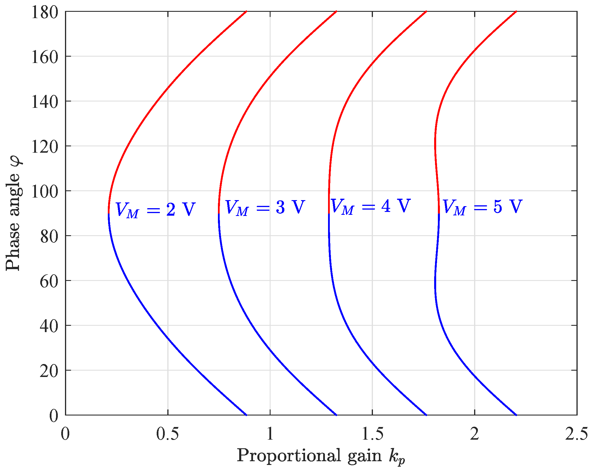
Figure 7 shows the stability boundary resulted from solving (
25) with respect to the proportional gain
for values of the duty cycle within the operating range
and for a value of the ramp compensator amplitude
V. Within one sinewave signal one has 2000 switching cycles. Therefore, the plot was generated using 1000 values of the duty cycles and the critical values of
were registered in terms of
D. In particular, for
V, the critical value of the proportional gain guaranteeing that all the eigenvalues lie inside the unit circle for all values of the operating duty cycle is about
. This is in perfect agreement with the numerical simulations presented in
Section 3. If
is increased, the critical value of the proportional gain also increases and the stability region gets wider as depicted in
Figure 8. In particular, for
V, the critical value of the proportional gain is about
, for
V, is about
and for
V, it is about
. Notice that for a fixed switching period
T, changing the ramp amplitude is equivalent to changing its slope.
As stated previously, in DC-AC inverters, the reference voltage is a time varying sinusoidal signal and accordingly the steady-state quasi-static duty cycle
D is given by (
8). In such a situation, the phase
is a quasi-static parameter like
D. Solving (
9) in terms of the phase angle
, one gets two critical values of the phase angle that can be expressed as follows
These closed expressions for the critical phase angles at which SO develops explain the observation made in
Section 3. In terms of the inverter gain
and its maximum value
, the expressions of the phase angles are given by
The stability boundary of the system is plotted in
Figure 9, in terms of the proportional gain
of the voltage controller and the phase angle
. Vertical dashed lines in
Figure 9 indicate this theoretical critical value for the set of parameter values shown in
Table 1. For each specific union of
and
curves, it can be noted that there is a turning point at the left side of the union. The system will be stable at the left of the turning point and will exhibit an SO phenomenon at its right side. For instance, let
; the system is stable during the entire sinewave cycle as already observed in
Figure 5a. When the proportional gain
is increased beyond its critical value, SO takes place within a certain phase interval, the length of which is determined by the intersection points between vertical lines corresponding to specific values of
and the two curves of
and
. Notice that the length of the SO interval gets larger when the proportional gain increases. For instance, for
, it is expected from
Figure 9 that the system will exhibit SO in the phase interval
which is in close agreement with the numerical simulation depicted in
Figure 5b. For
, the expected SO interval is
which is in close agreement with
Figure 5c and for
, the expected SO interval is
which is in close agreement with
Figure 5d.
The estimated values of the critical phase angles from
Figure 9 defining the SO interval differ slightly from the numerical simulation result in
Figure 5. The discrepancies between the theoretically predicted values in
Figure 9 and the ones obtained from numerical simulations depicted in
Figure 5 can be attributed to two main factors. The first one is the use of the quasi-static approximation. The second one is the fact that at the point where bubbling develops its amplitude is extremely small making it invisible in the scale used for representing the complete waveforms of the duty cycle during one entire sinewave cycle. By zooming close the critical values of
, more accurate data can be obtained and discrepancies decrease significantly.
As has been shown in
Figure 8, the maximal value of the proportional gain
guaranteeing stability during the entire the sinewave cycle depends on the ramp amplitude
. Therefore, the critical phase angle curves depicted in
Figure 9 are also obtained for different values of
and the results are depicted in
Figure 10. For each ramp amplitude
, a value of the proportional gain
selected at the left of the corresponding turning point will guarantee no presence of SO during the entire sinewave cycle. Note that as the ramp amplitude
increases the maximal value allowed for the proportional gain
also increases.


