Article

High-Pressure Sensors Based on Laser-Manufactured Sintered Silicon Carbide

by
Stefano Salvatori
1,*,
Gennaro Salvatore Ponticelli
1,
Sara Pettinato
1,
Silvio Genna
2 and
Stefano Guarino
1
1
Engineering Faculty, Niccolò Cusano University, Via don Gnocchi 3, 00166 Rome, Italy
2
Enterprise Engineering Department, University Tor Vergata, Via del Politecnico 1, 00133 Rome, Italy
*
Author to whom correspondence should be addressed.
Appl. Sci. 2020, 10(20), 7095; https://doi.org/10.3390/app10207095
Submission received: 4 September 2020 / Revised: 8 October 2020 / Accepted: 10 October 2020 / Published: 13 October 2020
(This article belongs to the Special Issue Laser Manufacturing of Advanced Materials)

Abstract

:
In this work Sintered Silicon Carbide (S-SiC) samples have been used to fabricate fiber-optic-coupled pressure sensors. The sensor structure reproduces a low-finesse Fabry–Perot (FP) interferometer. Laser manufacturing of cylindrical S-SiC samples was performed to define the thin membrane geometry of sensors. FP cavity is defined by the end-face of a single mode fiber and the S-SiC diaphragm surface. Hence, pressure is evaluated by measuring the cavity depth by a dedicated optoelectronic system coupled to the single mode fiber. Exploiting the excellent properties of S-SiC, in terms of high hardness, low thermal expansion, and high thermal conductivity, realized devices have been characterized up to 20 MPa. Experimental results demonstrate that produced sensors exhibit a non-linearity around ±0.6%F.S. and a high input dynamics. The all-optic sensing system proposed in this work would represent a good alternative to conventional solutions based on piezoelectric effects, overcoming the drawback related to electromagnetic interference on the acquired signals. In addition, the mechanical characteristics of S-SiC allow the use of the sensor in both automotive and aerospace hostile environments as pressure monitors in combustion engines.

Graphical Abstract

1. Introduction

Laser material processing represents a powerful tool in the modern manufacturing industry. Laser cutting is the most common industrial application of lasers, as well as welding, drilling, and marking processes, which have reached the right maturity to be accepted as standard tools in modern industry. Moreover, in recent years laser processing of materials also opened new perspective in additive manufacturing and micro-fabrication [1]. This trend is driven by the development of new applications as well as the increasing adoption of advanced ceramics in already established applications due to superior material and performance properties. However, it is worth noting that these properties are also the ones that do not allow obtaining accurate geometries using conventional machining techniques in a simple, cheap, and time-effective way [2]. In this context, lasers appear to be a promising technology with respect to ordinary material removal methods, because the machining operation is carried out without any contact between the laser system and the part, therefore ensuring the elimination of cutting forces, tool wear, and machine vibration [3]. In fact, the process efficiency depends on the thermal and optical properties of the material, allowing also hard or brittle materials, such as ceramics, to be machined. Moreover, lasers can be used for different applications, from the ablation of advanced ceramics [4], to the hardening of structural materials [5], to the joining of hybrid structures [6], as well as to the milling of composites [7], therefore demonstrating a very high versatility. Compared to other techniques, it is worth to mention that laser represents a unique manufacturing tool for ultra-hard material processing, such as diamond [8]. Indeed, laser allows to locally heat and ablate diamond allowing the realization of optics tailored to the specific application [9], as well as to induce a local transformation of diamond into graphite for the fabrication of all-carbon sensors with novel contact structures [10,11,12].
Silicon Carbide (SiC) represents the unique solid compound of silicon. Since the end of the 19th century, mass-produced SiC powder has been used as an abrasive in grinding wheels and abrasive applications in general. In addition, one of the early application of SiC ceramics was as high-durable brake discs for high-performance vehicles. With modern technology, high-quality SiC ceramics are produced [13]. Such materials have peculiar chemical and physical properties, such as high strength, ultra-high hardness, high elastic modulus, high resistance to thermal shock, low thermal expansion, superior chemical inertia, high thermal conductivity, and excellent corrosion resistance [14]. For these reasons SiC finds application in the manufacture of high precision machine parts. SiC ceramics are widely used, for example, in the automotive industry for the manufacture of brakes and clutches [15], but are also used for the fabrication of plates in bulletproof vests. In addition, due to its physical properties, one of the first applications of SiC was as lighting arrester in electric power distribution systems. Nowadays, modern microelectronics technology in advanced semiconductor industries has also made it possible to apply SiC in crystalline form for the manufacture of electronic components able to operate in high power and high frequency fields. SiC devices find application especially in harsh environments where silicon shows its limits mainly due to a reduced bandgap compared to SiC. Moreover, due its excellent characteristic, most of research works are related to the fabrication of micro-electro mechanical systems (MEMSs) based on crystalline SiC.
The high hardness and low fracture toughness make crystalline SiC (c-SiC), as well as sintered SiC (S-SiC), difficult to machine. In fact, conventional diamond grinding or turning is characterized by high cost and high wear of diamond tools [16]. In addition, when micro-sized features are required several technological issues can arise, e.g., low quality surfaces and cracks formation. In recent years, different unconventional techniques have been investigated to respond to the increasing demand of machining of advanced ceramic materials. Specifically, electrical discharge machining (EDM) and laser beam machining are the main alternatives investigated in the experimental works. However, materials can be machined by EDM whether their electrical conductivity is greater than 10−2 S/cm [17]. Ceramics generally does not satisfy this requirement. In fact, SiC ceramics exhibit a typical electrical conductivity of about 10−15 S/cm, even if it can be tailored to display very diverse values within a range from 10−11 to 107 S/cm [18], but this is not the case. In order to allow EDM of these materials, an electrically conductive secondary phase is usually added to the insulating matrix [19]. On the other hand, focused pulsed lasers offer a virtual solution due to the fact that their effectiveness is independent of the mechanical and electrical properties of the machined materials [20].
MEMSs represent the field in which the peculiar physical properties of SiC and the versatility of laser treatments meet and several works also demonstrate the feasibility of miniature MEMS devices based on c-SiC [21]. Conventional methods of manufacturing SiC-based MEMS devices use the deep reactive ion etching and the electrochemical etching techniques [22]. In such cases, etching rate is very low and etching morphology is very poor. Conversely, laser manufacturing achieves higher etch rates and no additional mask material is necessary [23]. Moreover, laser ablation of SiC has been carried out with different pulse durations, from nanosecond to femtosecond regime, with higher etching rates [24]. Femtosecond lasers produce little contamination and low heat affected zone, but they are capable of slower removal rates if compared with nanosecond lasers [25]. Furthermore, the ns-pulsed lasers are machining systems cheaper than the fs-pulsed ones. Then, the most widely used laser system in practice is the nanosecond pulsed laser.
In this context, SiC-based MEMS sensors find application in several industrial fields, from avionics to automotive, from spacecraft systems to turbines’ parts. SiC has already been used for pressure sensors able to operate in high-temperature [26,27] and MEMS-based sensors and actuators [28,29], finding application in several fields, from automotive to aerospace, from healthcare to consumer electronics [30,31]. Indeed, as aforementioned, SiC represents the elective material for the fabrication of mechanical components able to work under severe conditions. Pressure sensors able to work in harsh environments are fundamental for combustion chambers and gas turbine engines monitoring [32]. Crystalline-SiC (c-SiC) piezoresistive and capacitive pressure sensors, as well as c-SiC diaphragms on silicon have been reported in the literature [26,33]. Moreover, polycrystalline SiC (poly-SiC) diaphragms on poly-SiC substrates for pressure sensors realization also demonstrated their effectiveness in high temperature conditions [34,35]. In our research, S-SiC membranes, fabricated by means of laser treatment able to engrave cylindrical samples, have been used for pressure sensors fabrication. The technological steps necessary for the realization of the sensitive elements are mainly reduced to the laser treatment of S-SiC, overcoming difficulties related to complex etching processing of c-SiC, as well as lowering the costs related to the pristine material growth.
Guaranteeing immunity to electromagnetic interference, fiber-optic pressure sensors [36] and Fabry–Perot (FP) interferometric sensors [37,38,39] have been proposed to operate in hostile and aggressive media. The feasibility of a low-finesse FP pressure sensor has been demonstrated for thin diamond membranes [39]. Adopting the same optoelectronic detection set-up, in this work thick cylindrical samples of S-SiC ceramics have been used to fabricate fiber-optic FP pressure sensors. A fiber laser apparatus was employed to ablate S-SiC creating a hole and leaving a flat diaphragm with defined thickness. The FP cavity is represented by the end-face of a single mode fiber (SMF) and the S-SiC diaphragm surface. Deforming the S-SiC membrane, the external pressure is measured evaluating the cavity length by means of the optoelectronic system coupled to the SMF and able to acquire the light interference signal. Sensor pressure sensitivity and full-scale range can be properly designed adjusting diaphragm diameter and thickness. The proposed structure would represent a valid alternative for the fabrication of pressure sensors able to work in the harsh environments the S-SiC ceramics sustains.

2. Materials and Methods

2.1. Sintered SiC Laser Processing

Sintered SiC samples (BC-4 SiC, Bettini Textile Division, LC, Italy) used in this work were obtained through dry molding process of high-purity SiC powder. All cylindrical samples, see Figure 1, have a diameter of 5 mm and 2 mm in height. Table 1 summarizes their main characteristics.
A ns-pulsed fiber Yb:YAG laser source (1064 nm, 30 W, mod. YLP-RA30-1-50-20-20, by IPG Photonics, MI, Italy), with a galvanometric scanning head (by LASIT SpA, NA, Italy) equipped with a flat-focusing F-Theta lens (by LINOS, QIOPTIQ, Goettingen, Germany) with focal length of 160 mm has been used for S-SiC processing. Table 2 summarizes the main characteristics of the laser-treatment apparatus.
Preliminary tests were conducted at scanning speeds between 500 and 2000 mm/s, at maximum light power (minimum repetition rate of 30 kHz). In order to evaluate the influence of the process on the manufacturing, three different scanning strategies have been verified: LINE, NET and CROSS, whose meaning is clarified with the scheme reported in Figure 2. High-resolution images of treated samples by scanning electron microscopy (SEM) are illustrated in Figure 3. The smoothest surface was obtained by means of the CROSS strategy at a scan-speed of 1000 mm/s. The other strategies show surfaces with higher levels of damage as well as a higher roughness. Indeed, high scanning speeds (2000 mm/s) do not allow to obtain a uniform surface remaining visible the effect induced by each laser-pulse. Conversely, at lower scan-speed smoother surfaces are gained thanks to a better overlapping of laser pulses.
Based on the preliminary investigation, S-SiC samples were laser treated according to the process parameters’ combination reported in Table 3. Laser processing was performed in order to ablate each S-SiC cylinder realizing the desired diaphragm diameter and thickness. A picture of an example of laser-processed sample is reported in Figure 4a. In this sample, a 3 mm in diameter hole was realized up a depth of 1.9 mm, hence a membrane 100 µm thick, with a removal rate of about 3.1 mg/min, which is to be considered for micromachining operations [20,40]. Moreover, a digital microscope (Hirox KH8700, River Edge, NJ, USA) was used to analyze the morphology of laser-treated regions. The 2D profile reconstruction of treated sample is shown in Figure 4a (bottom).

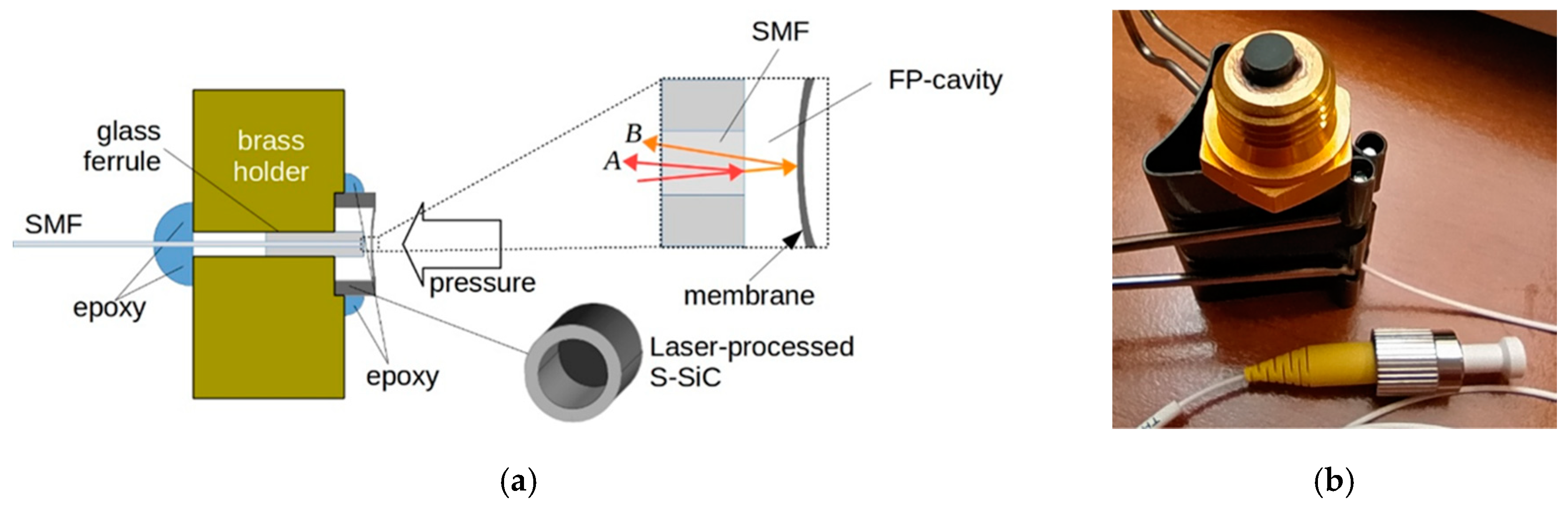
2.2. Low-Finesse Fabry-Perot Pressure-Sensor Structure and Measurement Set-Up

The schematic configuration of the fiber-optic Fabry–Perot pressure sensor is illustrated in Figure 5a. A single-mode fiber (SMF, SMPF0215-FC, with a mode field diameter = 10 μm @ 1550 nm; a cladding diameter = 125 μm; a coating diameter = 245 μm, by Thorlabs Inc., Newton, NJ, USA), is coupled to the laser-formed S-SiC membrane. FP cavity is represented by the fiber end-face and the inner surface of S-SiC diaphragm. As described in the previous section, S-SiC membrane is obtained by means of laser-ablation process of pristine cylindrical samples. As depicted in Figure 5a, laser light propagating into the SMF is partially reflected at the SMF facet (red arrow, A), whereas light transmitted at fiber output is reflected by the SiC diaphragm surface (orange arrow, B). Reflected beams propagating back into the fiber will generate an interference spectrum.
Laser-engraved S-SiC sample was fixed with epoxy to a ¾ inches full brass male cap holder used for mounting in a high-pressure-chamber used for sensor characterization. To assure SMF-membrane alignment, the brass holder was machined to create a through-pass hole (Ø 1.8 mm) and a 0.5 mm deep engrave for sample housing. The SMF, terminated with a glass ferrule (1.8 mm in diameter), was then inserted into the though-pass hole and positioned in front of the diaphragm surface. Finally, fiber was fixed to the brass sensor holder with epoxy.
For samples with a hole diameter around 2 mm, the ferrule was inserted until it touched the side walls of the engraved S-SiC cylinder. As shown in Figure 4b, due to the V-groove shape of the laser-treated cylinder, SMF face-end membrane distance was around 100 µm, assuring a good collection of reflected beams. Conversely, for samples with hole larger than ferrule diameter a different approach has been adopted. In this case, ferrule-terminated fiber was inserted into the brass holder/S-SiC system until it touched the surface of the membrane. Then, with a micrometric handling system, the fiber head was removed by 100 µm and finally fixed with epoxy resin. An example of mounted SMF-terminated S-SiC sample is reported in Figure 5b.
The experimental arrangement for characterizing the S-SiC pressure sensor is shown in Figure 6. The optoelectronic system is composed of a fiber-coupled laser diode operating at 1550 nm, an InGaAs photo-diode, and a 3-ports optical circulator (LPSC-1550-FC, FGA01FC, and 6015-3, respectively, by Thorlabs Inc., Newton, NJ, USA). Laser light enters in port 1 of the circulator and is emitted toward S-SiC sensor whose SMF is connected to port 2. Reflected light, hence interference signal, exits from port 3 and it is detected by the fiber-coupled photodiode. A current-to-voltage converter (PDA200C, Thorlabs Inc., Newton, NJ, USA) and a digital voltmeter (Keithley 2700 series, Tektronix Inc., Beaverton, OR, USA) are used for interference light intensity acquisition. As described in [39], for sensor characterizations, a hydraulic table top test pump is used to impinge a stationary pressure on sensor membrane and measuring the inlet pressure with a digital test gauge connected to the pump reference port.

3. Results and Discussion

Several S-SiC membranes have been fabricated with thickness ranging from 100 µm to 300 µm and diameter from 2.0 to 3.5 mm. Good results have been gained for membrane diameters around (2.4 ± 0.05) mm. Figure 7 shows experimental results for a (160 ± 10) µm thick membrane (S1 sample).
As shown in Figure 7a, in the 0–10 MPa range photocurrent amplitude displays the expected behavior of an interference signal given by [41]:
I ( λ , d ) = A 2 + B 2 + 2 A B c o s ( 4 π d λ )
where d is the cavity length and λ (= 1550 nm) the wavelength of light emitted by laser-diode, whereas A and B are the intensities of light reflected at the fiber end-face and the inner diagram surface, respectively (see Figure 5a). The observed signal periodicity corresponds to a λ/2 diaphragm shift, i.e., 775 nm. Continuous red line represents best fit of data according to Equation (1). Up to a pressure of 1.5 MPa, a monotonic behavior of the photocurrent signal is observed, confirming the feasibility of the fabricated sensing element (see Figure 7b). In the 0–1 MPa range, the sensor shows a full scale range non-linearity lower than 4%.
In order to evaluate sensor performances in terms of non-linearity and repeatability, according to Equation (1), fit of data reported in Figure 7 has been used to compile a look-up table (LUT) relating the photocurrent amplitude to the diaphragm deflection. Due to the non-monotonic nature of Equation (1), repeated measurements were performed increasing the pressure from 0 to about 10 MPa. Results are summarized in Figure 8a, where each point refers to pressure values recorded in correspondence of the photocurrent threshold values (i.e., membrane displacement) saved in the LUT. Obtained results displayed almost the same values at each test within the ±20 kPa (error bars for data in the figure are within the symbols). The sensor displays a good linearity, with a slope 0.163 nm/kPa (i.e., 16.3 nm/bar). In order to quantify the linearity error, the residuals between experimental and estimated values were evaluated by linear fit of data of Figure 8a. Results, reported in Figure 8b, depict that errors are lower than ±20 nm, i.e., ±0.6% on the investigated full scale range.
The same characterization has been performed for a (260 ± 10) µm thick diaphragm (sample S2). Figure 9 summarizes the experimental results where membrane deflection Δd was evaluated at voltages corresponding to a phase shift of interference signal of 0°, 45°, 90°, 135°, and 180°. As expected, sensor sensitivity of 0.038 nm/kPa is lower than that found for the S1 thinner membrane. Moreover, in the investigated 0–30 MPa range, non-linearity is around 3% of the full scale.
As depicted in Figure 5a, diaphragm is compressed towards the fiber end-face by the applied pressure. Being the optical fiber core diameter much lower than the diaphragm diameter, optical interference is mainly induced by the center deflection of membrane. Assuming a uniform thickness t for the membrane, under a uniformly distributed pressure difference ΔP between the two membrane surfaces, the deflection of the circular sensor diaphragm, with a radius r, at the center position is given by [42]:
Δ d m a x = 12 64 ( 1 ν 2 ) E r 4 t 3 Δ P
where E and ν are Young’s modulus and Poisson’s ratio for S-SiC, respectively. Experimental results reported in Figure 8 and Figure 9 allow to evaluate an effective value for E/(1-ν2) around 600 GPa. In particular, taking into account errors on diameter and thickness evaluation, a (610 ± 160) GPa value is found for S1 membrane, whereas a (570 ± 110) GPa value is obtained for S2 sample. In both the two cases, Young’s modulus would be between the one declared for S-SiC sample used in this work (see Table 1) and what reported for crystalline silicon carbide [14], stating the existence of a phase change induced by laser treatment performed to engrave the specimen.

4. Conclusions

Pressure sensors are widely used in various areas. In addition, it is often necessary to have pressure sensors made of materials suitable for use in hostile environments for particular applications. Due to its peculiar characteristics SiC is a suitable material for the realization of pressure sensors to be used also in hostile areas. In this work, fiber optic coupled pressure sensors were manufactured and characterized using S-SiC membranes with diameter from 2.0 to 3.5 mm and thickness ranging from 100 µm to 300 µm, obtained through laser ablation of uncontaminated samples. Experimental results show good performance for membrane with diameter around (2.4 ± 0.05) mm. In particular, for the membrane thickness (160 ± 10) µm the experimental results show a monotonic change in the acquired amplitudes ΔIph in the range 0–1 MPa, with a full scale non-linearity around 4%. A further characterization of the sensor has been performed in a wider pressure range (0–10 MPa) and the acquired photocurrent trend shows the expected sinusoidal trend of an interference signal. Moreover, the sensor shows good linearity (0.163 nm/kPa, i.e., 16.3 nm/bar), with linearity errors of less than ±20 nm, i.e., ±0.6% on the full scale investigated. For a second sample (S2 sample) with a (260 ± 10) µm thick diaphragm, the same characterization was carried out. In this case, non-linearity of about 3% of full scale was observed in the range 0–30 MPa and the sensitivity of the sensor (0.038 nm/kPa) is lower than that of the first sample, as expected. Moreover, experimental results allowed to estimate a Young’s modulus between the value measured for pristine S-SiC sample and the one reported for crystalline SiC, stating a possible phase change induced by the laser treatment used to realize sensor’s membrane.

Author Contributions

Conceptualization, S.S. and S.G. (Stefano Guarino); investigation methodology, G.S.P., S.P., and S.G. (Silvio Genna); sample fabrication and material characterization, G.S.P. and S.G. (Silvio Genna); sensor fabrication, S.P. and S.S.; optoelectronic measurement set-up, S.P. and S.S.; validation, S.S. and S.G. (Stefano Guarino); writing—original draft preparation, S.S., S.P., and S.G.P.; writing—review and editing, S.S. and G.S.P.; supervision, S.S. and S.G. (Stefano Guarino); funding acquisition, S.G. (Stefano Guarino). All authors have read and agreed to the published version of the manuscript.

Funding

This research was funded by POR-FESR LAZIO 2014–2020, grant number A0114-2017-13737 CUP F35F18000050007.

Acknowledgments

The authors would like to thank Armando Piccardi for insightful discussions on the measurement set-up as well as on experimental results.

Conflicts of Interest

The authors declare no conflict of interest. The funders had no role in the design of the study; in the collection, analyses, or interpretation of data; in the writing of the manuscript, or in the decision to publish the results.

References

  1. Steen, W.M.; Mazumder, J. Laser Material Processing, 4th ed.; Springer: London, UK, 2010. [Google Scholar]
  2. Tuersley, I.P.; Jawaid, A.; Pashby, I.R. Review: Various methods of machining advanced ceramic materials. J. Mater. Process. Technol. 1994, 42, 77–390. [Google Scholar] [CrossRef]
  3. Chryssolouris, G. Laser Machining: Theory and Practice; Springer: New York, NY, USA, 1991. [Google Scholar]
  4. Leone, C.; Genna, S.; Tagliaferri, F.; Palumbo, B.; Dix, M. Experimental investigation on laser milling of aluminium oxide using a 30W Q-switched Yb:YAG fiber laser. Opt. Laser Technol. 2016, 76, 127–137. [Google Scholar] [CrossRef]
  5. Ponticelli, G.S.; Guarino, S.; Giannini, O. An Optimal Genetic Algorithm for Fatigue Life Control of Medium Carbon Steel in Laser Hardening Process. Appl. Sci. 2020, 10, 1401. [Google Scholar] [CrossRef] [Green Version]
  6. Ponticelli, G.S.; Lambiase, F.; Leone, C.; Genna, S. Combined Fuzzy and Genetic Algorithm for the Optimisation of Hybrid Composite-Polymer Joints Obtained by Two-Step Laser Joining Process. Materials 2020, 13, 283. [Google Scholar] [CrossRef] [Green Version]
  7. Leone, C.; Papa, I.; Tagliaferri, F.; Lopresto, V. Investigation of CFRP laser milling using a 30W Q-switched Yb:YAG fiber laser: Effect of process parameters on removal mechanisms and HAZ formation. Compos. Part A Appl. Sci. Manuf. 2013, 55, 129–142. [Google Scholar] [CrossRef]
  8. Komlenok, M.S.; Kononenko, V.V.; Ralchenko, V.G.; Pimenov, S.M.; Konov, V.I. Laser Induced Nanoablation of Diamond Materials. Phys. Procedia 2011, 12, 37–45. [Google Scholar] [CrossRef] [Green Version]
  9. Kononenko, T.V.; Ralchenko, V.G.; Ashkinazi, E.E.; Polikarpov, M.; Ershov, P.; Kuznetsov, S.; Yunkin, V.; Snigireva, I.; Konov, V.I. Fabrication of polycrystalline diamond refractive X-ray lens by femtosecond laser processing. Appl. Phys. A 2016, 122, 152. [Google Scholar] [CrossRef]
  10. Komlenok, M.; Bolshakov, A.; Ralchenko, V.; Konov, V.; Conte, G.; Girolami, M.; Oliva, P.; Salvatori, S. Diamond detectors with laser induced surface graphite electrodes. Nucl. Instrum. Methods Phys. Res. Sect. A 2016, 837, 136–142. [Google Scholar] [CrossRef]
  11. Salvatori, S.; Rossi, M.C.; Conte, G.; Kononenko, T.; Komlenok, M.; Khomich, A.; Ralchenko, V.; Konov, V.; Jaksic, M.; Provatas, G. Diamond detector with laser-formed buried graphitic electrodes: Micron-scale mapping of stress and charge collection efficiency. IEEE Sens. J. 2019, 19, 11908–11917. [Google Scholar] [CrossRef] [Green Version]
  12. Girolami, M.; Conte, G.; Trucchi, D.M.; Bellucci, A.; Oliva, P.; Kononenko, T.; Khomich, A.; Bolshakov, A.; Ralchenko, V.; Konov, V.; et al. Investigation with β-particles and protons of buried graphite pillars in single-crystal CVD diamond. Diam. Relat. Mater. 2018, 84, 1–10. [Google Scholar] [CrossRef] [Green Version]
  13. Tanaka, H. Silicon carbide powder and sintered materials. J. Ceram. Soc. Jpn. 2011, 119, 218–233. [Google Scholar] [CrossRef] [Green Version]
  14. Smith, T.P.; Davis, R.F. Silicon Carbide. In Encyclopedia of Materials: Science and Technology; Buschow, K.H.J., Cahn, R., Flemings, M., Ilschner, B., Kramer, E., Mahajan, S., Veyssiere, P., Eds.; Elsevier Science Ltd., Pergamon Press: Oxford, UK, 2001; pp. 8497–8502. [Google Scholar]
  15. Yamada, K.; Mohri, M. Properties and Applications of Silicon Carbide Ceramics. In Silicon Carbide Ceramics—1; Sömiya, S., Inomata, Y., Eds.; Springer: Dordrecht, The Netherlands, 1991. [Google Scholar] [CrossRef]
  16. Ji, R.; Liu, Y.; Zhang, Y.; Dong, X.; Chen, Z.; Cai, B. Experimental research on machining characteristics of SiC ceramic with end electric discharge milling. J. Mech. Sci. Technol. 2011, 25, 1535–1542. [Google Scholar] [CrossRef]
  17. König, W.; Dauw, D.F.; Levy, G.; Panten, U. EDM-future steps towards the machining of ceramics. CIRP Ann. Manuf. Technol. 1988, 37, 623–631. [Google Scholar] [CrossRef]
  18. Román-Manso, B.; Domingues, E.; Figueiredo, F.M.; Belmonte, M.; Miranzo, P. Enhanced electrical conductivity of silicon carbide ceramics by addition of graphene nanoplatelets. J. Eur. Cer. Soc. 2015, 35, 2723–2731. [Google Scholar] [CrossRef]
  19. Pachaury, Y.; Tandon, P. An overview of electric discharge machining of ceramics and ceramic based composites. J. Manuf. Process. 2017, 25, 369–390. [Google Scholar] [CrossRef]
  20. Guarino, S.; Ponticelli, G.S.; Giannini, O.; Genna, S.; Trovalusci, F. Laser milling of yttria-stabilized zirconia by using a Q-switched Yb:YAG fiber laser: Experimental analysis. Int. J. Adv. Manuf. Technol. 2018, 94, 1373–1385. [Google Scholar] [CrossRef]
  21. Shi, Y.; Sun, Y.; Liu, J.; Tang, J.; Li, J.; Ma, Z.; Cao, H.; Zhao, R.; Kou, Z.; Huang, K.; et al. UV nanosecond laser machining and characterization for SiC MEMS sensor application. Sens. Actuators A Phys. 2018, 276, 196–204. [Google Scholar] [CrossRef]
  22. Maboudian, R.; Carraro, C.; Senesky, D.G.; Roper, C.S. Advances in silicon carbide science and technology at the micro-and nanoscales. J. Vac. Sci. Technol. A Vac. Surf. Film. 2013, 31, 050805. [Google Scholar] [CrossRef]
  23. Pecholt, B.; Gupta, S.; Molian, P. Review of laser microscale processing of silicon carbide. J. Laser Appl. 2011, 23, 012008. [Google Scholar] [CrossRef]
  24. Kim, S.; Bang, B.S.; Ren, F.; d’Entremont, J.; Blumenfeld, W.; Cordock, T.; Pearton, S.J. High-Rate Laser Ablation for Through-Wafer via Holes in SiC Substrates and GaN/AlN/SiC Templates. J. Semicond. Technol. Sci. 2004, 4, 217–221. [Google Scholar]
  25. Duc, D.H.; Naoki, I.; Kazuyoshi, F. A study of near-infrared nanosecond laser ablation of silicon carbide. Int. J. Heat. Mass. Transf. 2013, 65, 713–718. [Google Scholar] [CrossRef]
  26. Okojie, R.S.; Ned, A.A.; Kurtz, A.D. Operation of α (6H)-SiC pressure sensor at 500 °C. Sens. Actuators A Phys. 1998, 66, 200–204. [Google Scholar] [CrossRef]
  27. Okojie, R.S.; Nguyen, P.; Nguyen, V.; Savrun, E.; Lukco, D.; Buehler, J.; McCue, T. Failure mechanisms in MEMS based silicon carbide high temperature pressure sensors. In Proceedings of the 2007 IEEE International Reliability Physics Symposium Proceedings. 45th Annual, Phoenix, AZ, USA, 15–19 April 2007; pp. 429–432. [Google Scholar] [CrossRef]
  28. Atwell, A.R.; Okojie, R.S.; Kornegay, K.T.; Roberson, S.L.; Beliveau, A. Simulation, fabrication and testing of bulk micromachined 6H-SiC high-g piezoresistive accelerometers. Sens. Actuators A Phys. 2003, 104, 11–18. [Google Scholar] [CrossRef]
  29. Yasseen, A.A.; Zorman, C.A.; Mehregany, M. Fabrications and testing of surface micromachined polycrystalline SiC micromotors. EEE Electron. Device Lett. 2000, 21, 164–166. [Google Scholar] [CrossRef]
  30. Reynolds, J.K.; Catling, D.; Blue, R.C.; Maluf, N.I.; Kenny, T. Packaging a piezoresistive pressure sensor to measure low absolute pressures over a wide sub-zero temperature range. Sens. Actuators A Phys. 2000, 83, 142–149. [Google Scholar] [CrossRef]
  31. Huang, R.; Zhang, Y.; Chen, X.; Nie, B. A Wireless Flexible Pressure Sensor for Human Motion Detection. In Proceedings of the 12th International Congress on Image and Signal Processing, BioMedical Engineering and Informatics (CISP-BMEI), Suzhou, China, 19–21 October 2019; pp. 1–5. [Google Scholar] [CrossRef]
  32. Di, H.; Shen, T. Mutual information of cylinder pressure and combustion phase estimation in spark ignition engines. Control Theory Technol. 2019, 18, 34–42. [Google Scholar] [CrossRef]
  33. Young, D.; Du, J.; Zorman, C.; Ko, W. High-Temperature Single-Crystal 3C-SiC Capacitive Pressure Sensor. IEEE Sens. J. 2004, 4, 464–470. [Google Scholar] [CrossRef]
  34. Trevino, J.; Fu, X.; Zorman, C.; Mehregany, M. Low-stress Heavily-Doped Polycrystalline Silicon Carbide for MEMS Applications. In Proceedings of the 18th IEEE International Conference on Micro Electro Mechanical Systems, 2005. MEMS 2005, Orlando, FL, USA, 30 January–3 February 2005; pp. 451–454. [Google Scholar] [CrossRef]
  35. Li, C.; Mehregany, M. A silicon carbide capacitive pressure sensor for high temperature and harsh environment applications. In Proceedings of the TRANSDUCERS 2007–2007 International Solid-State Sensors, Actuators and Microsystems Conference, Lyon, France, 10–14 June 2007. [Google Scholar] [CrossRef]
  36. Zhu, Y.; Wang, A. Miniature fiber-optic pressure sensor. IEEE Photonics Technol. Lett. 2005, 17, 447–449. [Google Scholar] [CrossRef]
  37. Jiang, Y.; Xu, J.; Yang, D.; Zhang, K.; Li, D.; Zhao, J. Miniaturized Fiber Fabry-Perot Interferometer for Strain Sensing. Microw. Opt. Technol. Lett. 2016, 58, 1510–1514. [Google Scholar] [CrossRef]
  38. Liu, J.; Jia, P.; Zhang, H.; Tian, X.; Liang, H.; Hong, Y.; Liang, T.; Liu, W.; Xiong, J. Fiber-optic Fabry–Perot pressure sensor based on low-temperature co-fired ceramic technology for high-temperature applications. Appl. Opt. 2018, 57, 4211–4215. [Google Scholar] [CrossRef]
  39. Salvatori, S.; Pettinato, S.; Piccardi, A.; Sedov, V.; Voronin, A.; Ralchenko, V. Thin Diamond Film on Silicon Substrates for Pressure Sensor Fabrication. Materials 2020, 13, 3697. [Google Scholar] [CrossRef] [PubMed]
  40. Parry, J.P.; Shephard, J.D.; Hand, D.P.; Moorhouse, C.; Jones, N.; Weston, N. Laser micromachining of zirconia (Y-TZP) ceramics in the picosecond regime and the impact on material strength. Int. J. Appl. Ceram. Technol. 2011, 8, 163–171. [Google Scholar] [CrossRef]
  41. Born, M.; Wolf, E. Multiple-beam Interference. In Principles of Optics, 6th ed.; Cambridge University Press: Cambridge, UK, 1980; Chapter 7.6. [Google Scholar]
  42. Timoshenko, S.P.; Woinowsky-Krieger, S. Symmetrical Bending of Circular Plates. In Theory of Plates and Shells, 2nd ed.; McGraw-Hill Higher Education: New York, NY, USA, 1964; Chapter 3. [Google Scholar]
Figure 1. Sintered SiC samples. All the laser treated samples had a diameter of 5 mm and 2 mm in height.
Applsci 10 07095 g001
Figure 2. (a) Schematic of the system used for sample laser-treatments. (b) Preliminary tests were used to evaluate the best scanning strategy: LINE, NET, and CROSS.
Applsci 10 07095 g002
Figure 3. Scanning electron microscopy (SEM) images of surfaces morphology of laser-processed samples with a pulse frequency of 30 kHz and 20 repetitions. (a) 2000 mm/s, LINE strategy; (b) 1000 mm/s, NET strategy; (c) 1000 mm/s, CROSS strategy.
Applsci 10 07095 g003
Figure 4. (a) An example of laser-treated S-SiC sample (top). Hole diameter is around 3 mm. The structure of the bottom of the hole reveals the cross method adopted during laser treatment. The 2D profile reconstruction obtained by means of digital microscopy analysis is reported on the bottom. (b) 2D profile reconstruction for a sample with a membrane with ~ 2 mm diameter and ~ 150 µm thickness. Dotted lines represent glass ferrule-terminated SMF inserted in the engraved S-SiC sample (see Section 2.1).
Applsci 10 07095 g004
Figure 5. (a) Schematic of sintered SiC sensor. Single-mode fiber (SMF) end-face and diaphragm represent the Fabry–Perot cavity. Interference signal is generated by reflected signal at fiber end (A) and SiC membrane (B). (b) Laser manufactured S-SiC sensor mounted on the brass holder used for the experimental characterizations.
Applsci 10 07095 g005
Figure 6. Picture of the measurement set-up used for S-SiC sensors characterizations at different values of inlet static pressure. On the right, a detail of the optoelectronic system used for interference signal measurement (see ref. [39] for more details).
Applsci 10 07095 g006
Figure 7. Photocurrent signal as a function of the applied pressure acquired for a 160 µm thick S -SiC diaphragm. (a) In the 0–10 MPa range the expected sinusoidal behavior stated by Equation (1) is clearly found. The period of signal corresponds to a λ/2 = 775 nm deflection of membrane. (b) The plot shows the absolute value of the relative photocurrent change obtained subtracting the value acquired at 0 Pa. In the investigated 0–1 MPa range sensor non-linearity is around 4%.
Applsci 10 07095 g007
Figure 8. (a) Diaphragm deflection as a function of pressure for a membrane 160 µm thick. (b) Residuals calculated by the difference of values of (a) and those calculated by linear best fit of data.
Applsci 10 07095 g008
Figure 9. Diaphragm deflection as a function of pressure for a membrane 260 µm thick.
Applsci 10 07095 g009
Table 1. Main characteristics of Sintered Silicon Carbide (S-SiC) samples used in this work.
CharacteristicsValueUnit
CompositionSiC99.6% wt
B4C0.6% wt
Diameter5 ± 0.2mm
Height2 ± 0.2mm
Density3.4g cm−3
Hardness26.0 ± 0.3GPa
Flexural strength530MPa
Elastic modulus400GPa
Compressive strength2200MPa
Fracture toughness4MPa m1/2
Thermal conductivity110W K−1 m−1
Max use temperature1300°C
Table 2. Main characteristics of the laser system used for S-SiC treatments.
CharacteristicsValueUnit
Wavelength1064nm
Pulse width50ns
Repetition rate30–80kHz
Pulse energy (30 kHz)1mJ
Beam qualityTEM00
M21.2–1.5
Focused beam diameter80µm
Scan area100 × 100mm2
Max scan speed5000mm s−1
Table 3. Laser operational process parameters for membranes fabrication.
ParameterValueUnit
Laser scan speed500mm s−1
Repetition rate30kHz
Scanning modeCROSS-
Number of repetition 150–75-
Laser fluence 2 ~ 20J cm−2
1 Fifty repetitions were used for obtaining a 150 μm thick membrane, while 75 for a 100 μm thick membrane. 2 Defined as the ratio between the laser pulse energy and the laser beam spot area (see Table 2).

