Review

Light Emitting Devices Based on Quantum Well-Dots

by
Mikhail V. Maximov
1,*,
Alexey M. Nadtochiy
1,
Sergey A. Mintairov
2,
Nikolay A. Kalyuzhnyy
2,
Natalia V. Kryzhanovskaya
3,
Eduard I. Moiseev
1,
Nikita Yu. Gordeev
2,
Yuriy M. Shernyakov
2,
Alexey S. Payusov
2,
Fedor I. Zubov
1,
Vladimir N. Nevedomskiy
2,
Sergei S. Rouvimov
4 and
Alexey E. Zhukov
3
1
Nanophotonics Lab., Alferov University, 8/3 Khlopina, 194021 St Petersburg, Russia
2
Ioffe Institute, 26 Polytechnicheskaya, 194021 St Petersburg, Russia
3
Department of Physics, National Research University Higher School of Economics, 16 Soyuza Pechatnikov, 190008 St Petersburg, Russia
4
Department of Electrical Engineering, University of Notre Dame, Notre Dame, IN 46556, USA
*
Author to whom correspondence should be addressed.
Appl. Sci. 2020, 10(3), 1038; https://doi.org/10.3390/app10031038
Submission received: 6 January 2020 / Revised: 25 January 2020 / Accepted: 27 January 2020 / Published: 4 February 2020
(This article belongs to the Special Issue Novel and Efficient Semiconductor-based Light Sources)

Abstract

:
We review epitaxial formation, basic properties, and device applications of a novel type of nanostructures of mixed (0D/2D) dimensionality that we refer to as quantum well-dots (QWDs). QWDs are formed by metalorganic vapor phase epitaxial deposition of 4–16 monolayers of InxGa1−xAs of moderate indium composition (0.3 < x < 0.5) on GaAs substrates and represent dense arrays of carrier localizing indium-rich regions inside In-depleted residual quantum wells. QWDs are intermediate in properties between 2D quantum wells and 0D quantum dots and show some advantages of both of those. In particular, they offer high optical gain/absorption coefficients as well as reduced carrier diffusion in the plane of the active region. Edge-emitting QWD lasers demonstrate low internal loss of 0.7 cm−1 and high internal quantum efficiency of 87%. as well as a reasonably high level of continuous wave (CW) power at room temperature. Due to the high optical gain and suppressed non-radiative recombination at processed sidewalls, QWDs are especially advantageous for microlasers. Thirty-one μm in diameter microdisk lasers show a high record for this type of devices output power of 18 mW. The CW lasing is observed up to 110 °C. A maximum 3-dB modulation bandwidth of 6.7 GHz is measured in the 23 μm in diameter microdisks operating uncooled without a heatsink. The open eye diagram is observed up to 12.5 Gbit/s, and error-free 10 Gbit/s data transmission at 30 °C without using an external optical amplifier, and temperature stabilization is demonstrated.

1. Introduction

InGaAs/GaAs quantum wells (QWs) and In(Ga)As self-organized quantum dots (QDs) are presently utilized as active areas of various high performance optoelectronic devices such as edge-emitting lasers [1], microlasers [2,3,4], solar cells [5,6,7,8,9], etc. The use of the quantum confinement effect permits tailoring density of states that governs all intrinsic characteristics of semiconductor material—wavelength of emitted or absorbed light, carrier lateral diffusion and capture, relaxation mechanisms, radiative lifetime, etc. Modification of the active area properties allows one to control and optimize the performance of optoelectronic devices (efficiency, threshold, output power, operation speed, etc.) as well as to develop devices based on novel principles such as single-photon light sources or quantum processing devices [9].
Both QWs and QDs possess a number of inherent advantages and disadvantages caused by their structural properties and energy band diagrams (see Table 1). In QD structures, carrier lateral transport is suppressed due to the efficient spatial localization in QDs of electrons and holes. In contrast, in QW structures, carriers can freely diffuse in the plane of QW. As a result, QD-based structures are less sensitive to epitaxy- or post-growth-related defects compared to their QW-based counterparts. However, in QD structures, optical gain/absorption is relatively low due to limited QD density and inhomogeneous broadening of the QD array. In QWs, optical gain/absorption is much higher. For GaAs-based structures, the emission wavelength of QDs can be much longer than that of QWs and covers telecommunication O-band (1.26 μm–1.36 μm). The formation of QDs is accompanied by efficient strain relaxation [1,10] that enables stacking 20 and more QD layers with high crystalline quality. In contrast, deposition of several InGaAs QWs (> 3 in the optical region around and beyond 1 μm, typical QW width and In compositions are 8–10 nm, and 15%–18%, respectively) results in the formation of the dislocation due to accumulation of excessive elastic strains in the semiconductor layers, and the use of complex strain compensation techniques is required [11].
Presently, high-quality InGaAs/GaAs QWs and QDs suitable for device applications are formed by molecular beam epitaxy (MBE) or metal-organic chemical vapor deposition (MOCVD). However even with the use of these up-to-date technologies, it is very challenging to fabricate a nanostructure with properties characteristic of an “ideal” 2D or 0D object.
During the growth of GaAs/AlGaAs QWs, monolayer high fluctuations can be formed at the lower and upper interfaces. At cryogenic temperatures, local thickenings of the QW results in carrier localization in the lateral direction and plays the role of shallow QDs [12,13]. In the case of InGaAs/GaAs QWs, there are fluctuations of the In composition that acts as localization potentials for electrons and holes [14]. Similar effects of QD-like emission from In-rich regions have also been observed in InAlAs/InP (see, for example [15]). Compositional and thickness fluctuations are much more enhanced in case of quaternary or quinary QWs, e.g., InGaAsN(Sb).
QD arrays are usually represented by narrow bandgap inclusions (islands) inside a wide bandgap matrix. However, these “geometrical” QDs do not necessarily show properties that are expected for “ideal” QDs with delta-function like the density of states. To fulfill this condition, the confinement energy for electrons and holes in QDs should be high enough to prevent carrier thermal evaporation from the ground state to excited states and continuum (wetting layer and matrix). In practice, this means that, on the one hand, the size of a QD should be large enough to provide sufficient localization energy of electrons and holes at the ground state. On the other hand, the QD size should not be too large to prevent the formation of a number of closely spaced electron and hole energy levels. For the device application, these conditions must be satisfied at room temperature, which implies that confinement energy of electrons and holes with respect to the wetting layer/matrix (and, ideally, first excited state) should exceed at least 3 kBT (where kB—Boltzmann constant). In addition, homogenous and inhomogeneous broadening of QD array also deteriorates its properties as compared to the case of an ensemble of “ideal 3D emitters”.
Given the above considerations, fabrication and studies of nanostructures, which properties are intermediate between QWs and QDs, are of special fundamental interest and beneficial for certain practical applications. Such nanostructures should combine useful properties of both QWs and QDs and, to some extent, be free of their disadvantages. Starting from the QW side, such InGaAs nanostructure can represent an InGaAs QW comprising In-rich regions and local thickenings, which are capable of localizing electrons and holes. Starting from the QD side, it can be implemented as a dense array of shallow InxGa1−xAs QDs inside the thin InyGa1−yAs layer (x > y). Two-dimensional QWs and 0D QDs are usually formed when the In content in the depositing InGaAs material is either low (x < 0.3) or high (x > 0.5), respectively. The growth and investigation of structural and optical properties of InxGa1−xAs layers with moderate In concentrations (0.3 < x < 0.5) is expected to be useful for the formation of the aforementioned nanostructures of intermediate 2D-0D dimensionality.
A number of research groups have investigated nanostructures that can be considered as intermediate cases between QWs and QDs. These structures were referred to as modulated quantum wells [16,17], as quantum wires [18,19,20,21,22,23,24], as ‘Wires-on-Well’ (WoW) [25,26], and as ‘Well-Island’ [27]. One approach is to use a dense array of small-sized QDs [21,28,29]. For instance, in references [28,29], the structures were grown by submonolayer migration-enhanced epitaxy on vicinal substrates with the amount of deposited InAs close to the critical value of 1.8 monolayers (ML). A blue shift and narrowing of the photoluminescence (PL) band with increasing misorientation angle was observed. The fact that QDs become smaller and more uniform in size was attributed to lateral confinement of QDs on terraces formed due to step bunching effect. In reference [21], the alignment of InAs QDs on very regularly formed multiatomic GaAs steps, produced by step bunching on vicinal (100) substrates, was studied. This approach was used for growing regular arrays of quantum wire (QWR) structures formed along the step edges.
Another approach to form nanostructures of mixed dimensionality is to apply MOCVD or MBE growth of InGaAs with low In composition [16,25,30]. Partial strain release results in the appearance of thickness and compositional modulations. Many groups rely on growth on vicinal substrates and step-bunching effect at the upper interface of the growing InGaAs layer. For instance, the initial stage of InGaAs growth by MOVPE on multiatomic-stepped GaAs structures was studied in [22]. It was found that in the initial stages of InGaAs growth, Ga and In atoms preferentially attach themselves to the bottom edges of the multiatomic steps. The key issues in the formation of InGaAs QWRs are the uniformity of the multiatomic steps and the large modulation in the lateral thickness of InGaAs on multiatomic-stepped GaAs structures.
As early as in 1997, it was demonstrated that the luminescence peak position strongly depends upon growth parameters and can be tuned in a wide spectral interval even for the same x and average thickness of the deposited InGaAs [31]. The samples were grown by submonolayer deposition of InAs and GaAs by MBE and had nominally the same composition (~31%) and thickness (~7 nm). However, for the sample grown in the alternating mode of group III and group V atoms, the maximum of PL emission was shifted by 120 meV towards lower energies with respect to the emission from the first sample grown in the continuous deposition mode.
In reference [30], the impact of substrate misorientation and the number of deposited In0.18Ga0.82As layers on strain relaxation mechanisms were studied. Multiple In0.18Ga0.82As/GaAs layers were deposited by MBE on exactly oriented substrates as well as on 2° misoriented towards the [0-11] direction GaAs substrates. In the case of the growth on nominal GaAs(100) surfaces, the strain relaxation was governed by dislocation formation. In contrast, the additional strain relaxation mechanism was revealed for vicinal GaAs(100) substrates. If the number of deposited In0.18Ga0.82As layers is less than 8, step bunching provided a mechanism for strain relaxation. In case the number of In0.18Ga0.82As layers exceeds 10, bunched corners along with two [051] and [0–1–5] directions also contribute to the strain relaxation in addition to the step bunching.
Morphology of the strained In0.3Ga0.7As (2–4 nm)/GaAs (2.7 nm)/GaAs0.6P0.4 (3 nm)/GaAs (2.7 nm) superlattices deposited on GaAs surfaces with different misorientations (0 and 6° off) was investigated in [19,25,26]. For both types of substrates, growth conditions were exactly the same. A significant layer undulation was observed in the case of a 6° misoriented substrate. This corrugation was attributed to step bunching and non-uniform precursor incorporation between steps and terraces. In contrast, the growth of the exactly oriented substrate resulted in flat morphology. The undulation effect was the most pronounced for InGaAs layers. As a result, a periodic array of InGaAs nanowires on planar wells was formed that was referred to as Wires-on-Well (WoW). Lateral periodicity of layer undulation was determined by TEM as 66 nm. The total height of the WoW was ~3.1 nm, and the minimum thickness of the InGaAs, at the boundary between one wire and the next one was ~0.71 nm. The wire width was about 48.6 nm. The WoW geometry can be tuned by changing equivalent thicknesses of InGaAs and GaAsP layers. An increase in the equivalent thickness of InGaAs results in the enhancement of the height of the wires. The wire width also increased with the InGaAs equivalent thickness, but this effect is less pronounced. Strain-balancing was crucial to maintain the periodicity of the InGaAs WoW array. The WoW photoluminescence peak shifted according to the size of InGaAs wires in optical region 1.15–1.3 eV, and the intensity was affected by the accumulation of lattice-mismatch stress.
In reference [20], the authors reported on nanostructures that they referred to as QWRs. Samples with QWRs were based on 40 QW/barrier pairs made of strain balanced In0.2Ga0.8As/GaAs0.85P0.15 on 6° misoriented GaAs substrate. Nominal QW thickness was 8 nm, and barrier thickness was 17 nm. The in-plane periodicity of the QWRs was 121 nm, the total height of the QWR was 13.6 nm, and the minimum thickness of the layer, at the boundary between one QWR and the next one, was 4.6 nm. Optical properties of QWRs were compared with a reference QW grown on the exactly oriented surface. Growth on the misoriented surface resulted in a broadening and a redshift of PL line from 1.26 eV to 1.22 eV. Radiative recombination was found to be less efficient in these QWRs than in reference QW grown on the exactly oriented surface.
Formation of In0.4Ga0.6As QWRs was demonstrated during the MBE growth on the (311)A surface [24]. The average height of the wires was found to be 4 nm; the PL maxima were at about 1.34 meV. The enhanced linewidth of the PL lines (>30 meV) was attributed to the size distribution of the quantum wires and the quality of the InGaAs/GaAs interfaces.
Recently, we have demonstrated a novel type of nanostructures that we refer to as quantum well-dots (QWDs). The QWDs represent a dense array of carriers localizing indium-rich regions formed inside In-depleted residual quantum wells by MOCVD deposition of 4–16 monolayers of InxGa1−xAs (0.3 < x < 0.5) on GaAs substrates (Figure 1). QWDs can be considered as nanostructures of mixed (0D/2D) dimensionality. The use of QWDs in single-junction GaAs solar cells enabled extending of long-wavelength edge of the spectrum of internal quantum yield from 860 nm up to 1100 nm, which resulted in a record high increment in the photocurrent (4.6 mA/cm2 for 20 QWD layers) for terrestrial spectra [32], which is making QWDs promising for photovoltaic applications.
Despite the rather interesting results obtained for photovoltaic converters based on various nanostructures of mixed dimensionality, including WoW, QWR, QWDs, etc. [25,26], the reports on light-emitting devices were scarce [27,31]. In this review article, we mostly focus on the application of QWDs to light emitting devices, describe their basic properties, and demonstrate fundamental advantages.

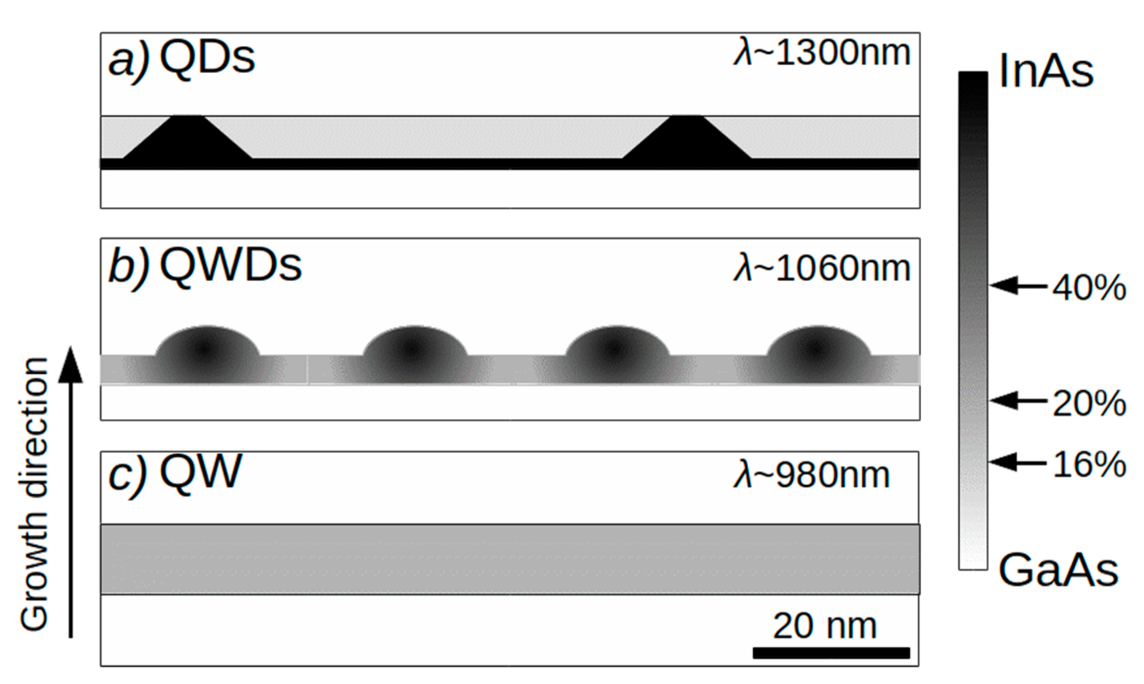
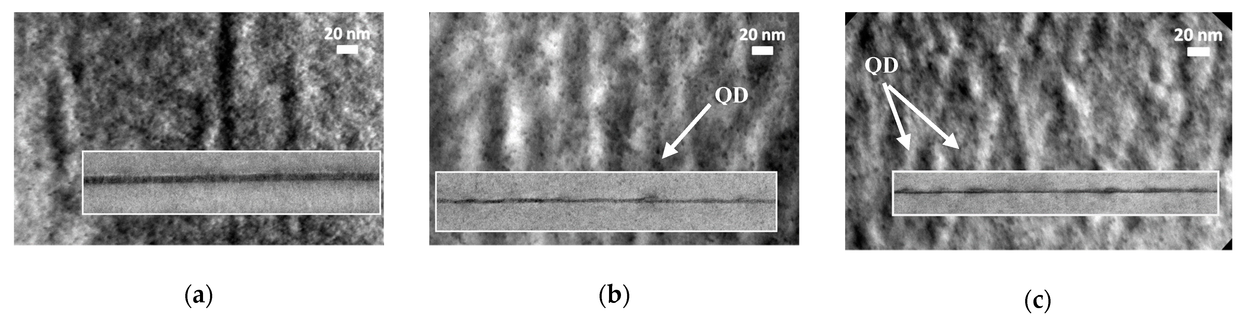
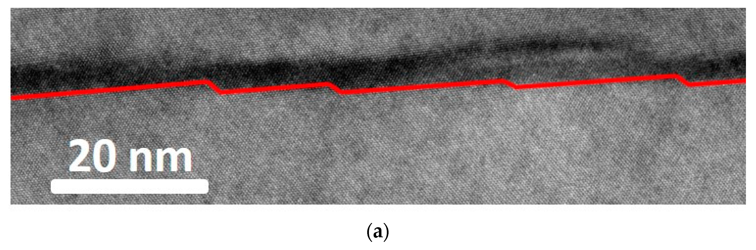
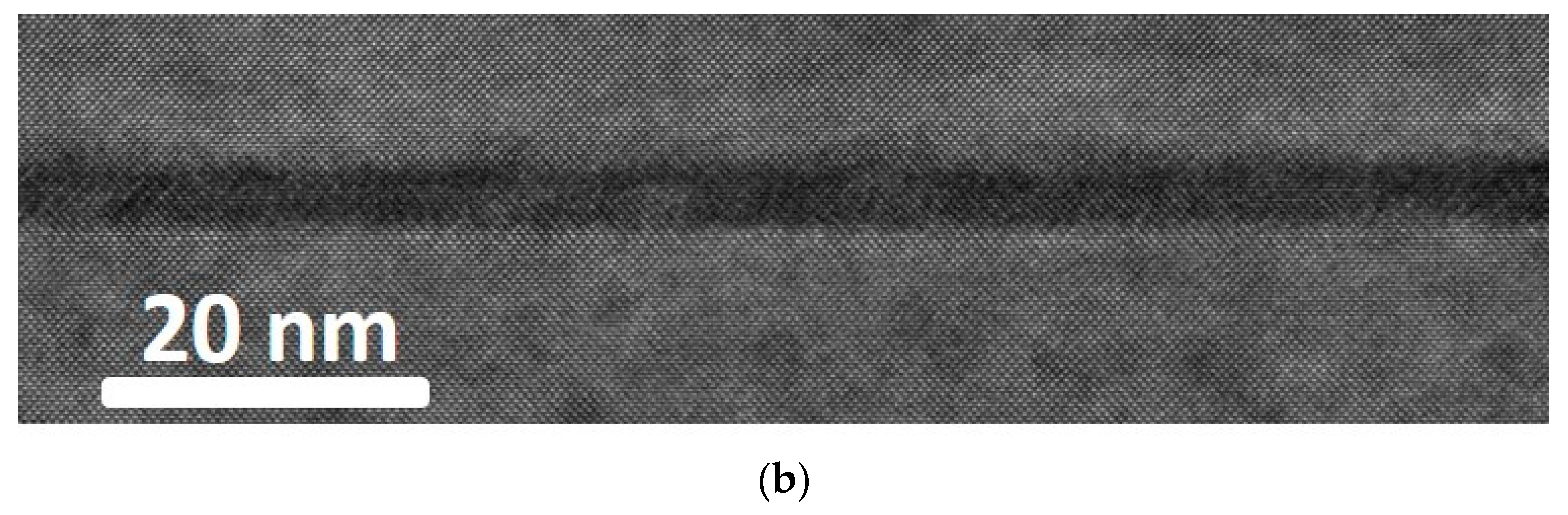
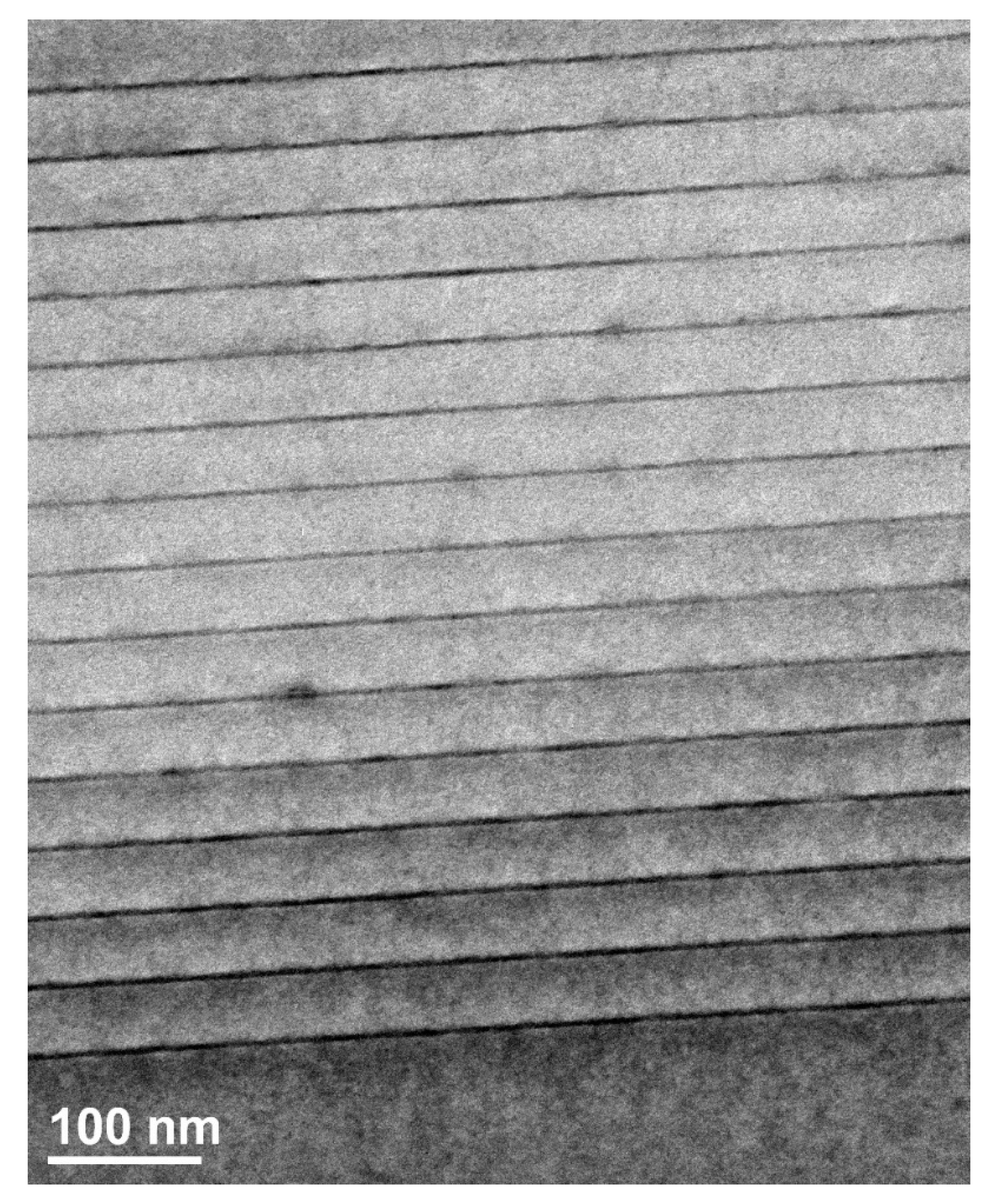
2. Growth and Structural Properties

The formation of QWDs takes place during the MOCVD deposition of a lattice-mismatched InGaAs thin film on the GaAs substrate. Structures have been grown on exact oriented (100) and vicinal (4–6° off) GaAs substrates using an MOCVD installation with a low pressure (100 mbar) horizontal reactor. Metal alkyls (trimethylgallium, trimethylaluminum, trimethylindium) and arsine were used as precursors. GaAs and AlGaAs layers were deposited at 700 °C, the ratio of molar flows of V to III group precursors is about 30, and 0.4 nm/s growth rate. InGaAs QWDs are formed at lowered growth temperatures 500–550 °C, the ratio of molar flows of V to III group precursors is about 30 and 0.2 nm/s growth rate. Compositional and thickness modulations appear due to surface migration of In atoms in the lateral strain fields. In other words, the appearance of In-rich islands is energetically favorable because of partial strain relaxation. On the one hand, elastic strain should be strong enough to cause such modulations. On the other hand, it should not be too high in order to avoid the transition to the Stranski–Krastanow growth mode and formation of conventional self-organized QDs. The strain energy depends both on the thickness and composition of the lattice-mismatched epitaxial material (i.e., the In content), and both parameters should be optimized. The most direct method to study the structural properties of InGaAs nanostructures is transmission electron microscopy (TEM). The combination of cross-section and plan-view TEM images allows one to determine the size, shape, and density of in-rich islands.
Let us consider the growth of InxGa1−xAs layer of different In concentrations (x) on GaAs substrate. Deposition of In0.2Ga0.8As results in the formation of a planar uniform layer. If the indium concentration exceeds 60%, the growth occurs in Stranski–Krastanow mode via the formation of the wetting layer on the top of which large-sized pyramid-shaped islands are formed. In both cases of low and high In contents, QWDs are not observed in TEM images. The window of In composition to grow QWDs is from 30 to 50%.
Figure 2 illustrates the impact of indium composition on structural properties of InGaAs layers formed on 6° misoriented GaAs (100) substrates. The strain fields caused by variation of indium composition are visualized as black-and-white contrast. Plan-view TEM images reveal the formation of islands with a higher In composition as compared to the In concentration in the surrounding InGaAs layer (residual QW). It is these islands that we refer to as quantum well-dots. The QWDs are aligned along the [1–10] direction, have a round or oval shape and lateral size (in case of In0.3Ga0.7As) of 10–20 nm. The islands tend to form nanowire-shaped clusters along the [1–10] direction, which corresponds to the direction of atomic steps [33,34]. This tendency is weakening with increasing the indium composition. The nanowire-like objects show periodicity in the [110] direction with a period of 20–40 nm. Note that the length of monolayer steps for 6° misoriented GaAs (100) surface is about 3 nm. The larger value of the found periodicity is due to the “step-bunching” effect [35] that occurs during the MOVPE growth on vicinal substrates [16].
QWD layer formed by deposition of In0.4Ga0.6As represents the larger lateral size of the islands—20–30 nm (Figure 2b). The tendency for the QWDs to merge into wire-like clusters along atomic steps is less pronounced as compared to the case of In0.3Ga0.7As. In addition to QWDs, there are also objects with a larger size, which can be considered as conventional QDs. However, the surface density of such QDs is much lower compared to that of the QWDs, so they do not significantly affect the optical properties of the sample, as will be shown below.
Lateral sizes of the QWDs and the QDs revealed from cross-section TEM (insets to Figure 2a–c) are in good agreement with the plan-view TEM data (Figure 2a–c). The average height of the QWDs for x = 0.4 is 3 nm, that means that the thickness modulation of the QWD layer is not high (about 30% of its average thickness). The QDs are much bigger in size than QWDs; their average lateral size is 30–40 nm, and the average height is about 6 nm.
Further increase in the In composition up to x = 0.5, i.e., an increase in the lattice mismatch, leads to significant growth of the density of QDs, whereas the density of QWD decreases. From the viewpoint of their geometrical dimensions, these QDs resemble conventional QDs formed in Stranski–Krastanow growth regime. The QDs do not align along with the atomic steps.
QWDs can be formed on the exact (100) oriented substrate as well, but their structural properties are strongly influenced by substrate orientation (Figure 3). In the case of the vicinal surface, the modulations of indium composition and layer thickness are much more pronounced; in other words, QWDs are better developed. Atomic steps existing on the vicinal surface facilitate island growth mode. Note that the thickness modulations often follow atomic steps (Figure 3a). For the exact oriented surface, the QWDs have smaller lateral size ~10 nm as compared to QWDs grown on 6° misoriented substrate (20–30 nm). The large-sized QDs are formed only on the misoriented surface, cover many atomic steps, and likely appear due to coalescence of individual QWDs. The impact of surface misorientation angle was also studied in [18]. InGaAs/GaAsP multiple quantum wells (MQWs) were grown by MOVPE on vicinal GaAs (001) substrates with different miscut angles of 0°, 2°, and 15° towards [110]. Growth on substrates with 2° and 15° miscut angles resulted in the formation of quantum wires and quantum dots as revealed by atomic force microscopy and photoluminescence.
Since the growth of QWDs is accompanied by a partial relaxation of elastic strain, there is no fast strain accumulation upon the stacking of QWD layers, and misfit dislocation formation is suppressed. This effect is similar to the case of stacking of the self-organized QDs, and is an advantage of QWDs as compared to QWs. Figure 4 shows TEM image of the sample with 15 vertically stacked QWD layers. The structure demonstrates high crystal quality, and no dislocations are observed. In contrast, vertical stacking of more than 3 InGaAs QWs with composition 15–20% would result in dislocation formation and drastic deterioration of optical quality. The possibility of dislocation-free stacking, a large number of QWD sheets is advantageous to obtain high optical gain/absorption in optoelectronic devices. In [20,26], 200 and 40 stacks of WoW and QWR with high optical and crystal quality were demonstrated, respectively. However, in both cases, careful strain balancing was applied.

3. Optical Properties

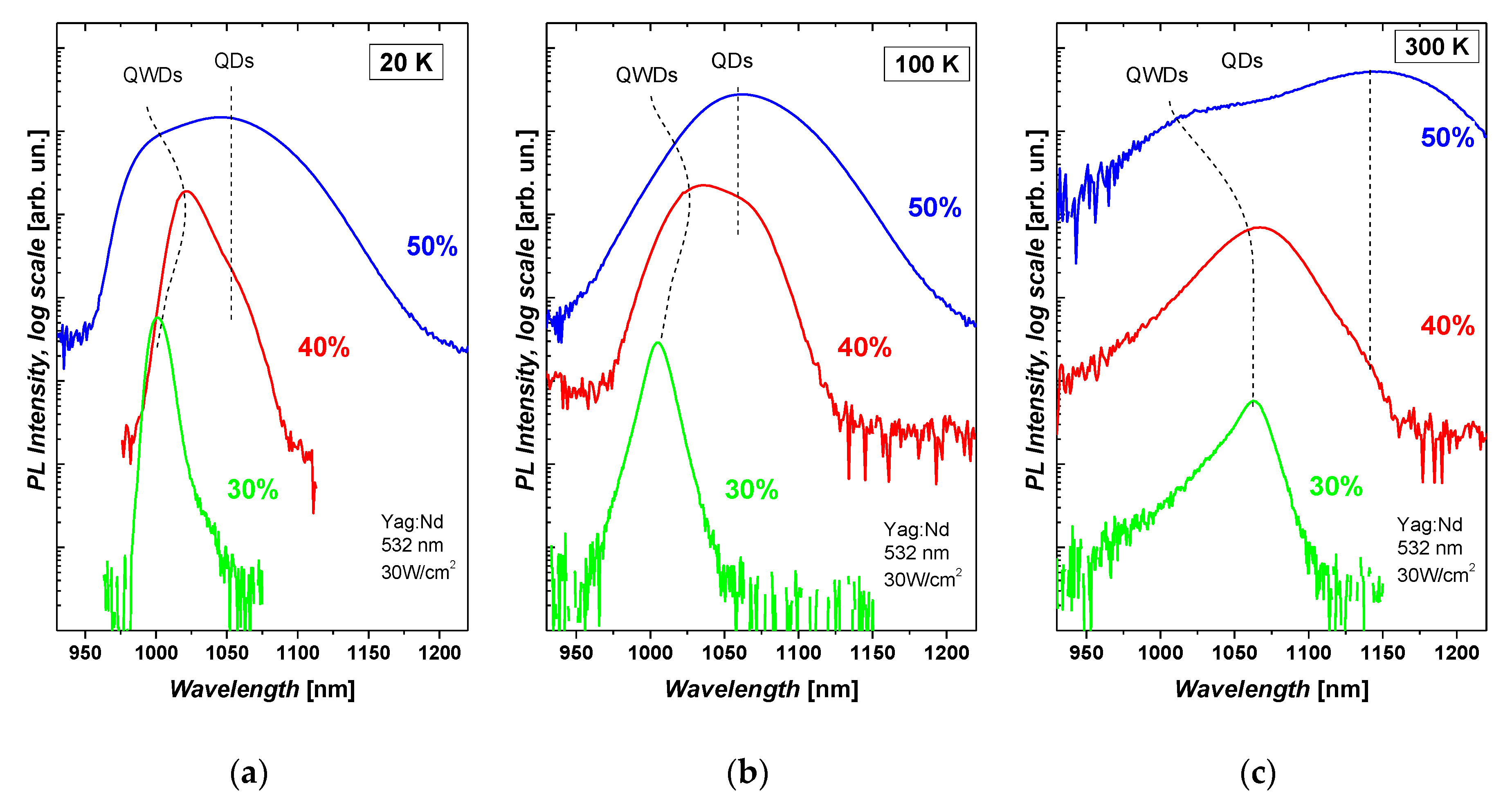
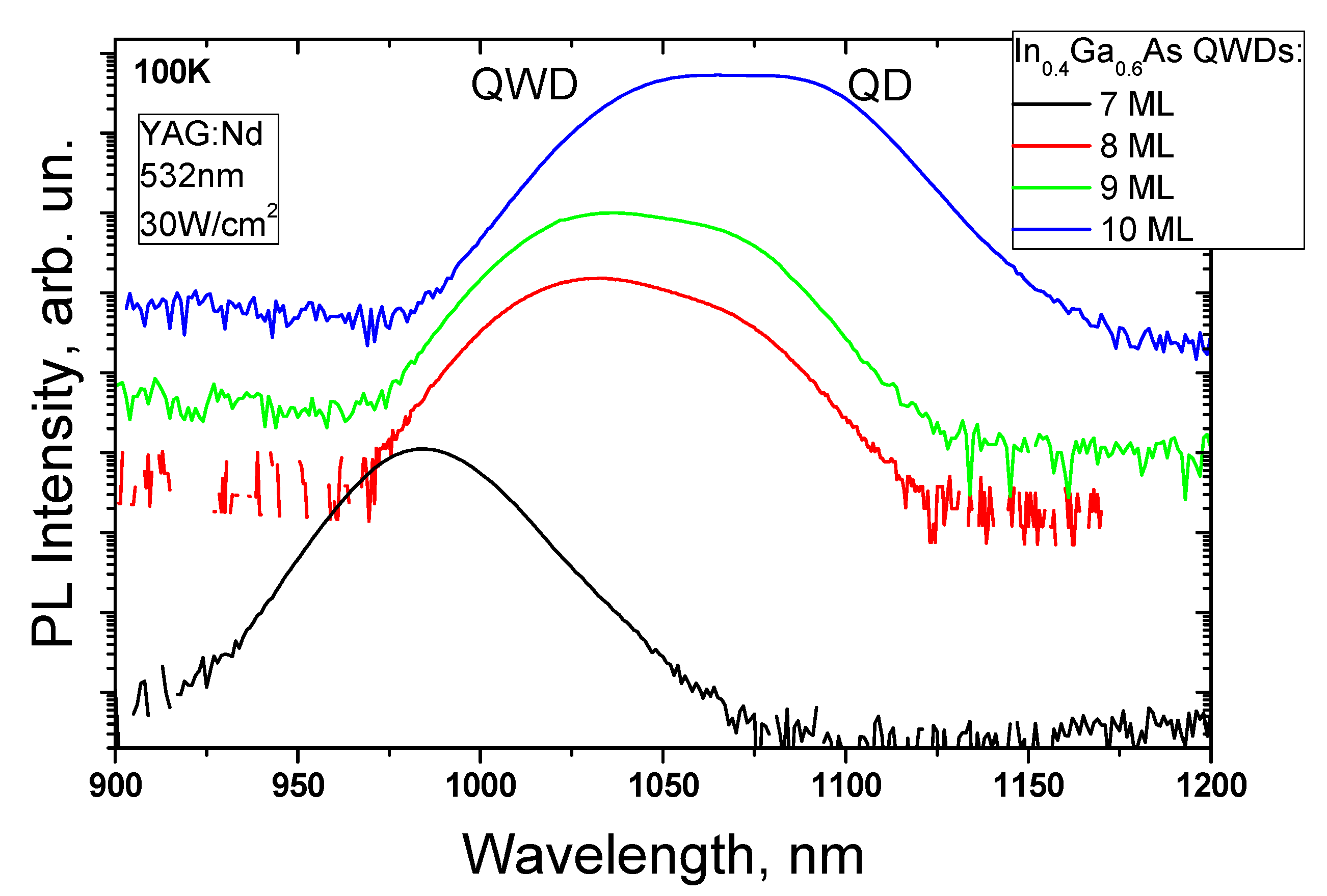
3.1. The Impact of Indium Composition and Average Layer Thickness on Photoluminescence Spectra

The existence of two types of quantum-sized objects with different sizes and correspondingly with different confinement energy (QWDs and QDs) results in a characteristic modification of photoluminescence (PL) spectra with temperature increase.
At low-temperature thermal escape of carriers from both types of localized states (QWDs and QDs) to the matrix is suppressed (Figure 5) and random (or non-equilibrium) population of the joint QWD/QD array is realized. The PL spectrum was taken at 20 K and moderate excitation power density is composed of ground-state emission from both QWDs and QDs and reflects their size distribution and density. Temperature raise opens the possibility of carrier transport between localizing objects resulting in a redistribution of intensities of the corresponding peaks in the PL spectrum. In the middle-temperature range (~80–150 K), it can be expected that carrier transport is controlled heavily by the activation energy of confined states (i.e., the energy gap between confined state and matrix) because carrier escape probability is increasing with decreasing activation energy of the confined state. This results in one-way carrier transport from QWDs with smaller confinement energy to QDs providing stronger confinement. Further increase in the temperature (180–300 K) leads to blurring of differences in the probability of carrier escape from QWD and QDs resulting in two-way carrier transport, or in other words, establishing of equilibrium population in joint QWD/QD ensemble according to Fermi–Dirac statistics.
The PL spectra of the samples with QWDs formed by the deposition of InxGa1−xAs with x = 0.3, 0.4, and 0.5 are in good agreement with the results of TEM studies. The structure with QWDs formed by the deposition of 16 monolayers (ML) of In0.3Ga0.7As demonstrates a narrow single PL peak (Figure 6a), pointing out that there are no other quantum-sized objects apart of QWDs. The peak is gradually red-shifted and broadened with temperature increases (Figure 6a–c).
PL spectra of QWDs formed by the deposition In0.4Ga0.6As show quite different behavior. At 20 K, the main PL peak is accompanied by a shoulder on the long-wavelength side pointing to the presence of two kinds of quantum-sized objects in the active area separated by a potential barrier. On the base of TEM studies, we attribute the shorter- and longer-wavelength peaks to emission from QWDs and QDs, respectively. The ratio of QWD-to-QD surface densities is estimated as ~10:1, according to the relative peak intensities in PL at 20 K. Temperature rising up to 100 K leads to gradual PL intensity redistribution from the QWD peak to the QD one, which is accompanied by a dramatic change in the PL spectrum shape (Figure 6b). However, further temperature increase results in reverse evolution of the spectrum—QD shoulder has nearly vanished, and only the main peak, which corresponds to QWDs, remains in the spectrum. One can conclude that the samples formed by the deposition of InGaAs with 40% indium concentration comprises QWDs as major quantum-sized objects, and there is an only small fraction of QDs, which are characterized by deeper localization energies. The PL signal from QDs state is noticeable only under the one-way carrier transport conditions in the temperature range 80–150 K.
In the case of the samples formed by the deposition of In0.5Ga0.5As, the increase in QD density revealed by TEM (Figure 2c) is confirmed by PL studies. In the low-temperature PL spectrum, one can see that peaks of QWDs and QDs have comparable intensities. With temperature increase up to 100 K, the contribution of shorter-wavelength peak (QWD) is vanished almost completely; however, further temperature increase (up to 300 K) results in recovery of its intensity (Figure 6c). The interpretation of such behavior, as well as in the previous case, is based on the existence of one-way carrier transport from QWDs to QDs in a middle-temperature range. However, in the case of 50% indium concentration, the QD density is higher than that of QWDs, and, correspondingly, the intensity of QWD related PL peak is relatively weak. Separate peaks due to different kinds of quantum-sized objects were also revealed in [18]. An extra emission was observed from the 2° and 15° off samples, and attributed to the photoluminescence from quantum wires and pyramidal self-controlled quantum-dots, respectively. These peaks were absent at the PL spectrum on 0° surfaces.
Thus, we can conclude that the increase of In composition of deposited InGaAs layer results in a systematic increase of the QD density in comparison to the density of QWDs, which agrees well with the data obtained by TEM studies. The impact of the increase in InGaAs thickness on QWD PL spectra is shown in Figure 7. The spectra were recorded at 100 K when the QD peak is the most pronounced. If the InGaAs thickness amounts to 7 ML, only the QWD peak is seen in the spectrum. With the increase in the nominal thickness of deposited InGaAs, the intensity of the QD-related PL peak also increases that reflect the growth of QD density, which is confirmed by TEM studies [36]. For the 10 ML thickness, the QD PL peak becomes as intensive as that from QWDs. Our results qualitatively agree with [37], where In0.15Ga0.85As QWs were grown on a GaAs(001) vicinal substrate with a miscut of 6° towards (111)A. Optical and structural investigation revealed the presence of step bunches at the upper interface of the QWs with thickness 20 nm and 30 nm. As step bunches were not present in the thinner QW (10 nm), the authors can conclude that the phenomenon is activated above a critical thickness of the InGaAs layer that depends on the growth parameters and the growth rate.
To conclude this part, tuning the InGaAs layer composition and thickness makes it possible to control QWD-to-QD density ratio and, correspondingly, optical properties of the samples.

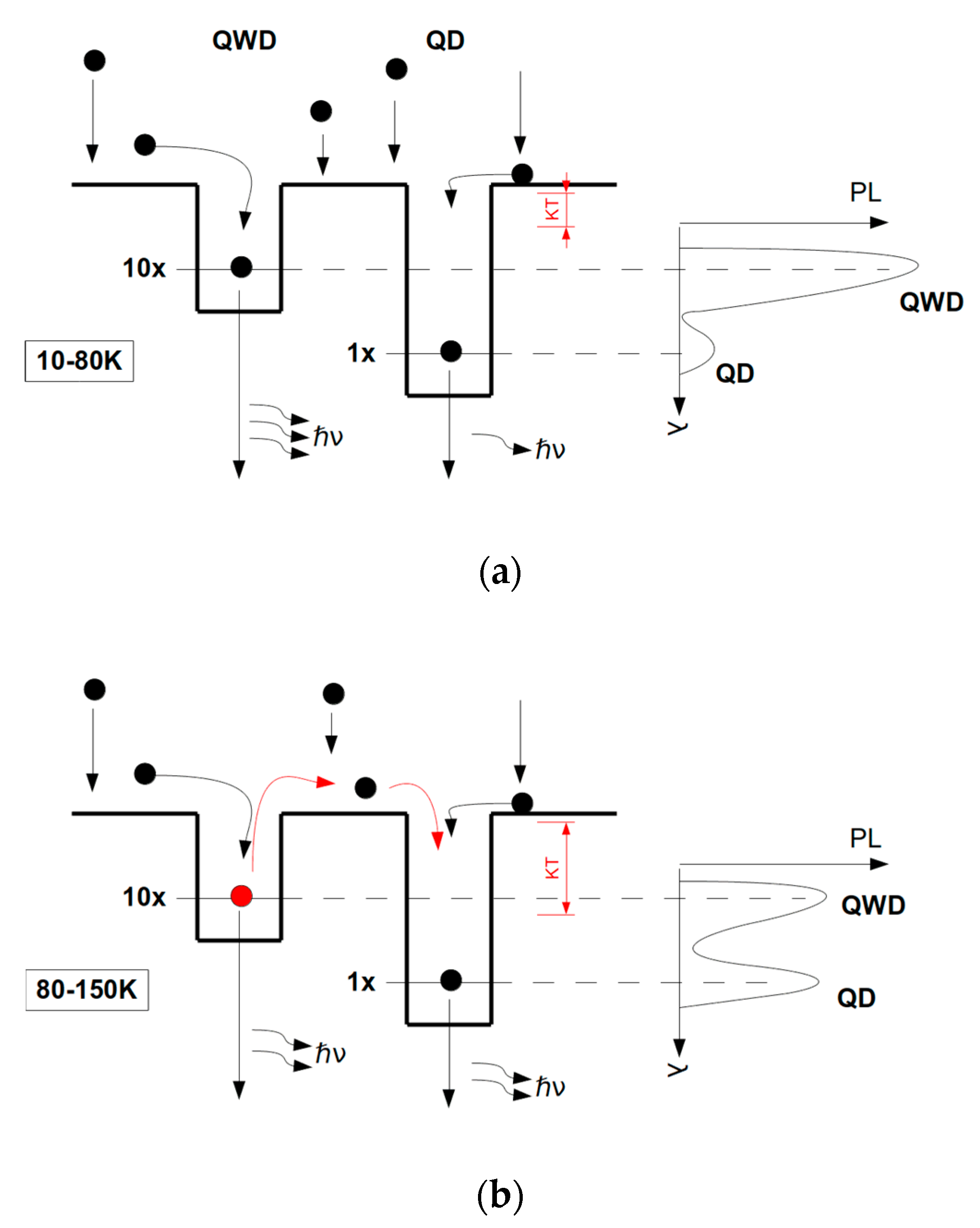
3.2. Lateral Carrier Diffusion in QWDs

Carrier diffusion plays an important role in understanding the performance and optimization of parameters of optoelectronic devices, particularly lasers and light-emitting diodes. The diffusion length sets the ultimate limit on the active device diameter. For this reason, a great effort has been dedicated to the development of fabrication technology for nanostructures with a smaller diffusion length [38,39,40]. The diffusion process is drastically influenced by the dimensionality of the active region: while 3D carrier diffusion is possible in a bulk unconfined active region, diffusion is restricted in a plane for a 2D quantum well, and to a single direction for a quantum wire. Ultimately, carrier localization in all three spatial directions in an ideal 0D QDs [41] affects different device characteristics, including the weak sensitivity to dislocations and etched sidewalls. Suppressed carrier diffusion in QDs has been indirectly proved in various experiments, such as improved scaling characteristics of ridge narrow stripe lasers [39], increased tolerance to radiation-induced damage [42,43], and improved performance of ultrasmall devices [44,45,46]. Recently, room-temperature lasing has been realized in QD based microdisks as small as 1 μm [47].
As it follows from the above consideration, QWDs are an intermediate case between the 2D and 0D situations. Carriers can be localized in the minima of the potential profile of the QWD layer due to inhomogeneities in its thickness and composition, even in case the potential profile is not purely zero-dimensional. Thus, the ability of charge carriers to diffusion is suppressed. As the temperature or the injection level is increased, more and more carriers are thermally evaporated into higher energy levels and continuum states. Even in unconfined energy states within the band, the carrier mobility and, therefore, the diffusion length is strongly reduced by scattering due to spatial inhomogeneities, as evidenced, e.g., in the AlGaN and InGaNAs material systems [48,49].
Carrier diffusion in different types of quantum sized nanostructures can be studied by using temperature-dependent PL from mesa arrays of different diameters [50]. The smaller the mesa size, the easier for the carriers to reach the mesa sidewalls and to recombine non-radiatively. The drop of the mesa luminescence intensities with a decrease in mesa diameter will reflect the enhancement of the role of non-radiative recombination at sidewalls.
Figure 8 compares integrated PL intensity measured at 77 K (a) and 290 K (b) for mesas of various diameters. The mesas arrays were formed by electron beam lithography and etching from three types of In(Ga)As/Ga(Al)As heterostructures having different active regions: InGaAs/GaAs 2D quantum wells, InGaAs/GaAs QWDs and InAs/InGaAs/GaAs 0D QDs [51]. Note that the latter QDs emit near 1.3 μm and; therefore, provide strong confinement of electrons and holes. The intensities for each type of structure are normalized to their values measured for the largest (10 μm in size) mesas either at 77 K (a) or at 300 K (b). At 77 K, the intensity of the mesa array with QDs is independent of the mesa diameter. This is due to the fact that the carries are localized inside the QDs and do not contribute to lateral diffusion, whereas carrier concentration inside the wetting layer and GaAs matrix is negligible [50].
Carrier diffusion and correspondingly surface non-radiative recombination is activated with temperature increase. At room temperature, the carrier concentration in the continuum states is enhanced, and the PL intensity of QD structure drops by about two times when the mesa diameter decreases down to 0.2 μm. In the case of mesas with QWD, the photoluminescence intensity (both at 77 and 290 K) exhibits faster deterioration with decreasing the mesa diameter as compared to QDs. This is explained by the fact that QWDs provides weaker carrier localization. The smallest mesa size showing detectable PL was 1 μm (at room temperature) or 0.3 μm (at liquid nitrogen). In the case of mesas with QW, photoluminescence was observed only in 6–10-μm in diameter mesas, whereas in the mesas with smaller sizes the luminescence was not detected. We conclude that carrier diffusion lengths in QWD structures are much shorter than in QW structures, which is in agreement with the suppressed carrier diffusion in disordered QWs [52]. This makes QWDs very advantageous for their use as an active area in compact nanophotonic devices (this will be discussed in more detail in Section 3.5).

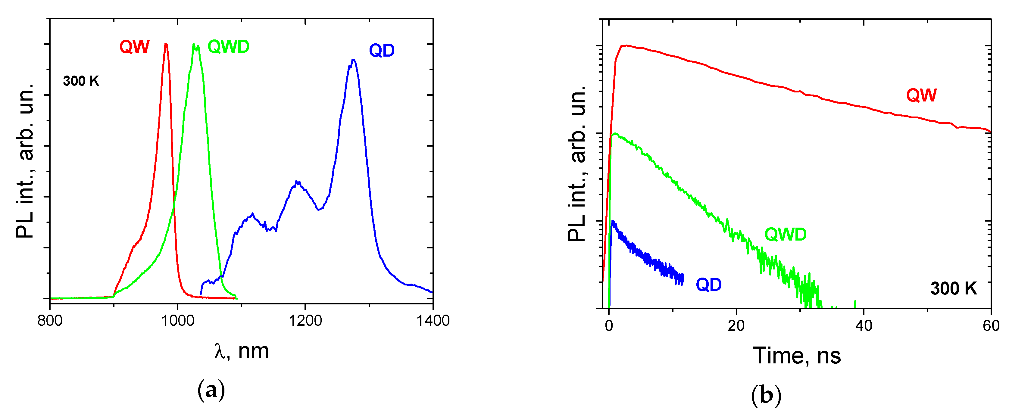
3.3. Dynamic Characteristics of QWDs

The quantum dimensionality naturally influences carrier relaxation and recombination processes in low dimensional structures. In this section, we compared results of time-resolved PL studies for 0D InAs/InGaAs/GaAs quantum dots [51], 2D InGaAs/GaAs quantum wells, and InGaAs/GaAs QWDs nanostructures of mixed (0D/2D) dimensionality.
The PL spectra at the CW excitation are demonstrated in Figure 9a. The spectrum of the QD sample contains a dominant peak at 1270 nm due to the emission from the ground-state optical transition as well as weaker peaks at higher energies due to the emission from the first and second excited-state transitions. The spectra of QWD- and QW-samples show intense peaks of the ground-state optical transition and weaker shoulder from the higher energy states. All the samples show high optical quality: the drop in integrated PL intensity with temperature increase from 78 K to 300 K is 3.2, 1.6, and 1.3 for QDs, QWDs, and QWs, respectively.
Figure 9b compares the temporal evolution of PL signal for the QD, QWD, and QW structures [53]. In case of QDs, the PL intensity temporal evolution can be well fitted by bi-exponential expression PL(t) = A1exp(τ1/t) + A2exp(τ2/t). The decay of PL signal is characterized by the fast component (τ1 = 1.1 ns) and slow component (τ2 = 7 ns). This agrees with previous estimations of PL decay time about 1 ns made for self-organized In(Ga)As QDs by several research groups [54,55]. The slow component is attributed to carrier radiative recombination from the QD ground state. It is generally believed that at room temperature, the carrier lifetime in semiconductors is limited by non-radiative recombination [56]. The obtained large value of PL decay time can be explained by carrier recapture in QD array [57,58] as well as to the absence of fast non-radiative recombination channels in the sample under study. The total PL decay time at 1/e level for the QD ground state transition is estimated as 6 ns.
QWD PL intensity temporal dependence can be fitted by a mono-exponential expression, which is ascribed to the absence of discrete high energy levels involved in carrier relaxation processed to the ground state. The PL decay time at 1/e level for ground-state transition is about 6 ns.
The QW structure shows the slowest PL decay with a characteristic time of 20 ns. This value is comparable with carrier radiative lifetime measured for QWs in the temperature range 150–250 K [59]. At higher temperatures, PL decay time is limited by non-radiative lifetime and is decreasing rapidly. Taking into account extremely high optical quality of the structures under study, which demonstrates room-temperature PL intensity comparable to the one at 78 K (to compare, in contrast, in [59], PL intensity degradation in the temperature range 10–250 K is higher than two orders of magnitude), one can suppose that non-radiative recombination processes are still not significant even at room temperature, and PL decay time corresponds to radiative recombination time.
Summarizing, the presented data show, that the carrier radiative recombination time is affected by structure dimensionality. The localization of charge carriers in QWDs results in the attraction of the carrier of opposite electrical charge and facilitates faster radiative recombination as compared to QWs.

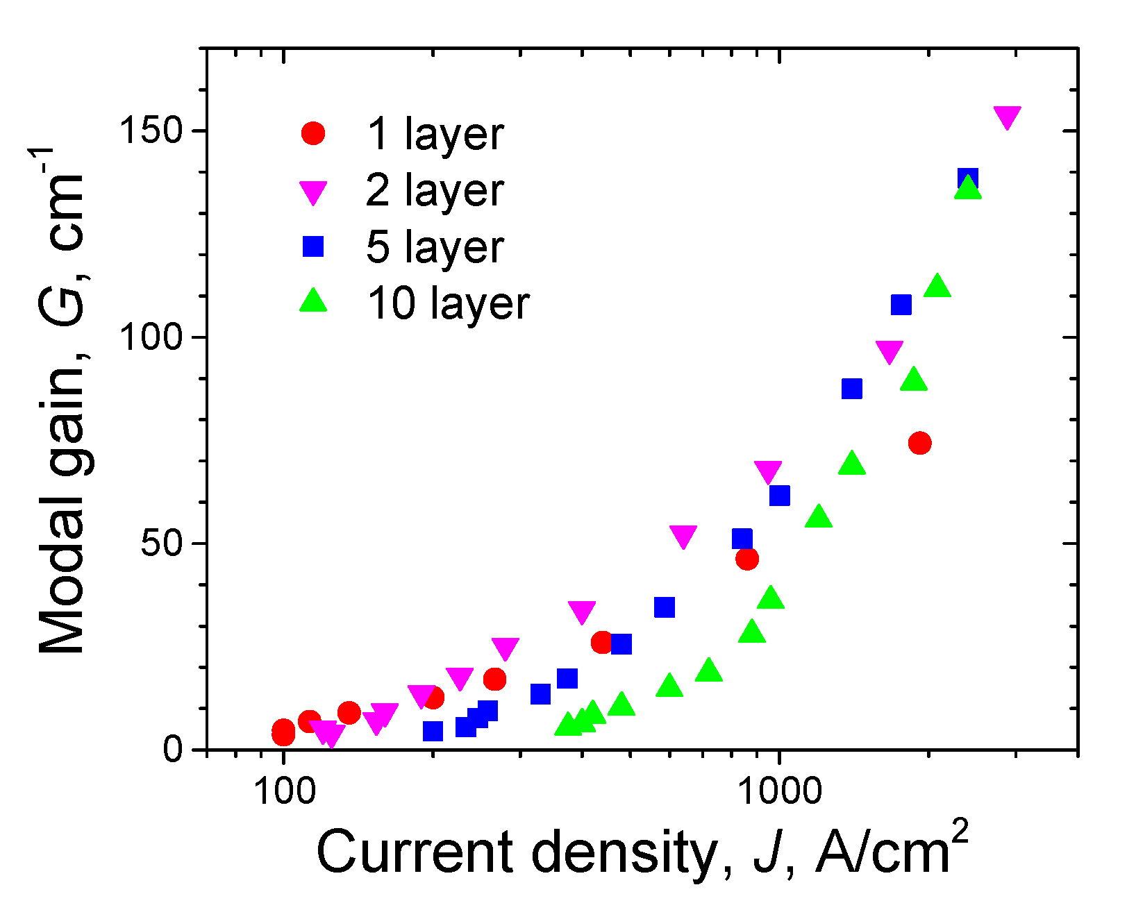
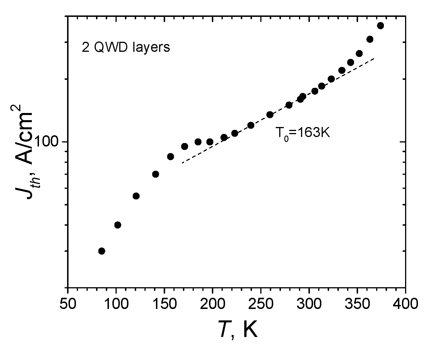
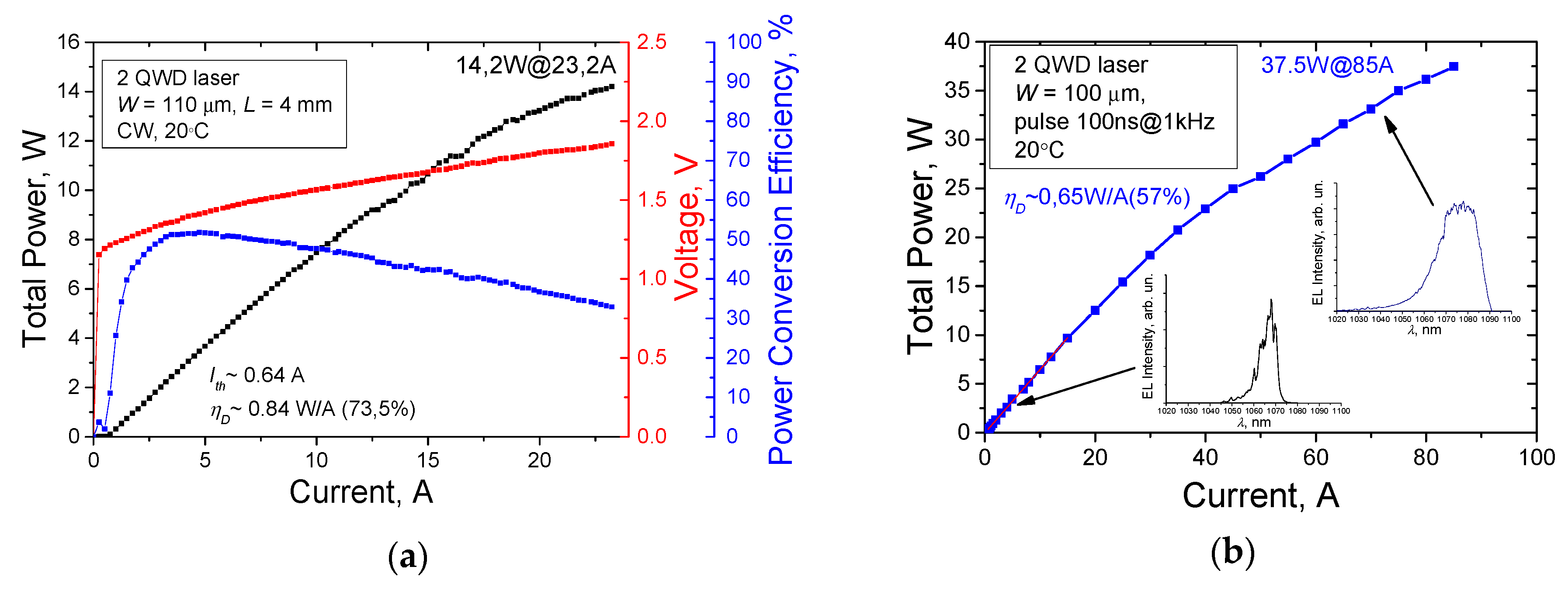
3.4. Edge Emitting Lasers

In this section, we describe properties of edge-emitting lasers based on QWDs.
The active area of semiconductor laser diodes, as well as device design, should be optimized for certain applications. For instance, high power QW lasers usually contain one or two QWs in the active area because the devices should have low internal losses. In the case of QD lasers, more QD layers (typically 5–10) are required to avoid gain saturation and switching to excited state lasing at high injection currents [60]. QWDs are an intermediate case between QWs and QDs, so the number of QWDs layers in the active area should be optimized.
The laser wafers with different numbers of QWDs in the active region (from 1 to 10) were grown by MOCVD on the GaAs substrates misoriented on 6° toward [111] direction. Each QWD layer was formed by the deposition of 8 ML of In0.4Ga0.6As. The QWD sheets were separated with 40 nm thick undoped GaAs spacers. The laser structures have undoped GaAs waveguides with a thickness of 0.68 μm not exceeding the third mode cut-off. The active region locates in the center of the waveguide, which ensures lasing on the fundamental transverse mode. The waveguide was sandwiched between p-type and n-type Al0.4Ga0.6As claddings having the thicknesses of 0.75 μm and 1.5 μm, respectively. For reducing the internal loss, the claddings doping levels of 2 × 1018 cm−3 were reduced down to 7 × 1017 cm−3 in the vicinity of the waveguide. The wafers were processed into broad-area lasers with 100-μm-wide shallow-mesa ridges with etching through the p-contact and partly through the p-cladding layers. The individual laser chips were mounted p-side down on copper heatsinks using an indium solder. No facet coatings were used.
The dependencies of laser characteristics on stripe length for devices with a different number of QWD layers are shown in Figure 10a–c. An increase in the number of QWD layers from 1 to 10 leads to a red-shift of the lasing wavelengths (from 1088 nm to 1117 nm in laser diodes of the longest cavity length), see Table 2. The red-shift was also observed in the electroluminescence spectra (Figure 11a). Such effect was not revealed in case of stacking strain balanced QWs [7,61,62], where peak positions do not depend on the number of the layers. We attribute this effect, at least partly, to the elastic strain redistribution in the multilayer QWD medium, similar to the case of stacking several layers of self-organized QDs [63,64,65].
A decrease in the cavity length leads to a blue-shift of the laser wavelengths. With decreasing cavity length output loss, increase and higher injection currents are required to achieve lasing. Since the maximum of gain spectra shifts to shorter wavelength with increasing injection current, the lasing wavelength also experiences a red-shift. The smaller the number of QWD layers, the larger the shift. For instance, as the cavity shortens from 4 mm to 0.25 mm, the wavelength changes by 20 nm in the case of 10 layers of QWDs, while for the laser based on single QWD layer, the wavelength shift is three times stronger (60 nm). In the case of the laser based on one QWD layer, the lasing line switches from the wavelength, which corresponds to the QWD ground state, to the wavelength of GaAs waveguide when cavity length decreases down to 200 μm. No lasing switching from the ground state to higher-energy states was observed for the devices with 2, 5, and 10 QWD layers.
The threshold current density (Jth) increased from 100 to 375 Acm−2 with an increase in the number of QWD layers from 1 to 10 (Figure 10b) that is typical for lasers based on both QWs and QDs [66]. Correspondingly, the threshold current density normalized to the number of the QWD layers (JQWD) decreased from 100 to 38 Acm−2. The values of threshold current densities for QWD lasers are larger than those in QD lasers [1,60,67] but smaller than in QW ones [68]. It should be noted that for 5 and 10 QWD layers, JQWD turned out to be almost the same. The dependence of the inverse differential efficiency (Figure 10c) on the cavity length was used to derive internal quantum efficiency and internal loss (Figure 10c). The internal losses increase from 0.7 to 2.4 cm−1 with an increase in the number of QWD layers from 1 to 10, whereas the internal differential quantum efficiency (ηi) weakly depends on the number of QWD layers of and amounts to about 80%. It should be noted that in the case of the lasers based on 1 and 2 QWD layers, the differential efficiency dramatically deteriorates when the cavity becomes shorter than 325 μm. In contrast, the lasers with 5 and 10 QWD layers do not show any drastic decrease in differential efficiency up to the shortest cavities of 125 μm.
The dependence of the modal gain on injection current (Figure 12) was calculated from the experimental dependence of threshold current density on external loss as described in detail in [69]. The maximal modal gain for the laser with 1 QWD layer of about 75 cm−1 is achieved at 1900 Acm−2. Higher gain values can be reached at higher currents, but the lasing switches to the electronic states of GaAs waveguide. The laser based on 2 QWD layer shows twice higher maximal modal gain (about 150 cm−1). For the lasers based on 5 and 10 QWD layers, the maximal modal gain was calculated to be 150 cm−1 as limited by the minimal cavity length used in the experiments. One can expect higher values of the maximal modal gain in multiply stacked QWD samples, even taking into account that the modal gain does not necessarily increase proportionally to the number of QWD layers.
Figure 13 shows a typical temperature dependence of the threshold current density of a QWD laser. In the temperature range of 220–320 K, the characteristic temperature T0 is 163 K. Typical characteristic temperatures of QD lasers with undoped active regions are 50–70 K, whereas the use of p-type modulation doping of active region allows one to increase it above 1000 K [60]. The characteristic temperature of the QW lasers typically slightly exceeds 100 K [70]. Note that QWD active region was undoped. Thus, the temperature stability of QWD lasers is comparable with the best QW lasers and exceeds that in QD lasers with the undoped active region.
In the temperature range of 120–200 K, the temperature dependence of the threshold current shows an N-shape [71], which can be explained by the presence of QDs in a joint QWD/QD array in the laser-active region (Section 3.1), when temperature increases above 100–150 K, the carriers start to evaporate from QWDs and are captured to QDs having deeper localization potential. In other words, QDs cause parasitic radiative recombination. Thus, additional current is required to compensate for this carrier loss, which leads to a “hill” in the temperature dependence of threshold current.
We note that stacking as many as 10 layers of QWD without any strain compensation, does not deteriorate the device performance (Table 2) as could be expected for QWs. To estimate the relative effect of non-radiative recombination centers on device performance, we studied the dependence of integrated electroluminescence intensity on injection current in lasers based on 1 and 10 QWD layers. The current component associated with the radiative recombination is characterized by a linear dependence of the integrated intensity on the injection current, whereas the non-radiative component is characterized by the quadratic dependence (Figure 14). At low injection levels, the non-radiative recombination determines the device characteristics. As the injection current increases, non-radiative recombination saturates and radiative recombination becomes the dominant one. The injection current, at which the behavior changes, depends upon the non-radiative centers’ density. In Figure 14, the crossover point is the intersection of the linear (radiative, P~J) and quadratic (non-radiative, P~J2) components. In both lasers, this current is quite similar (5 and 7 Acm−2 for the laser based on 1 and 10 QWD layers respectively). Thus, stacking up to 10 QWD layers does not result in a significant increase in dislocation density, which agrees with low threshold current density in that laser.
For achieving high-power operation, we have designed QWD lasers based on the CLOC (coupled large optical cavity) waveguide [72] and the active area based on 2 QWD layers. As seen from Figure 15, the devices based on 2 QWD layers provide the highest internal quantum efficiency, low internal loss, and low threshold current. The CLOC structures consist of a single-mode narrow passive waveguide optically coupled to a broadened active multimode waveguide. Due to the reduced optical confinement factor and increased optical losses, a selected parasitic transverse mode is eliminated from the lasing, ensuring transverse single-mode lasing. The active region consisting of two layers of InGaAs QWDs with 40 nm GaAs spacer was placed in the center of 1.3 μm undoped GaAs waveguide separated from the 220 nm GaAs passive waveguide by the 250 nm Al0.25Ga0.75As layer. The waveguide was designed to provide the elimination of the second-order mode. The thickness of the p-Al0.25Ga0.75As cladding layer was reduced down to 450 nm in order to improve heat dissipation from the active region. The laser wafer was grown with MOCVD, processed into 100 μm broad-area lasers in an abovementioned manner. The laser facets were covered by anti-reflecting (AR) and high-reflecting (HR) coatings and mounted p-side down on submounts. The broad area lasers with the cavity length of 4 mm showed CW output power of 14.2 W at room temperature (Figure 15a). Maximal wall-plug efficiency of 51.8% is achieved at 4.3 A. To the best of our knowledge edge-emitting, 1060 nm QW lasers demonstrate CW optical power as high as 18 W [73].
The pulsed output power of 37.5 W is achieved at room temperature (Figure 15b). The injection current is limited by the supply source. The decrease in differential efficiency at high injection currents (starting from ~40 A) is likely due to overheating and carrier pile-up in the active region as suggested by the redshift and broadening of the lasing spectrum, respectively.
To the best of our knowledge apart of the QWDs there are only a few works on light-emitting devices based on nanostructures with mixed dimensionality. In [31], significant depolarization of the heavy-hole-related electroluminescence was observed and attributed to in-plane strain fields caused by modulations of In composition. In reference [27], a special InGaAs-based well-island composite quantum-confined structure was demonstrated, and both super-wide and very uniform gain and power distributions were obtained. The spectral flatness of the output power reached 0.1 dB, and the gain bandwidth was broadened to six-folds broader than FWHM (full width at half the maximum) of the standard gain spectrum from a classic InGaAs quantum well under the same carrier density. The formation of the well-island composite quantum-confined structure was associated with the Indium-rich island effect in the material growth.
To conclude this part, QWD based edge-emitting lasers show a high optical gain, high differential efficiency, low threshold currents, low internal loss, and good temperature stability. They can find applications as efficient optical emitters for the spectral range around 1.1 μm. We expect that using advanced waveguide design (broad waveguides, thin top-emitter and contact layer, etc.), better heat dissipation, and up-to-date facet coatings will result in enhancement of output power levels.

3.5. Microdisk Lasers Based on QWDs

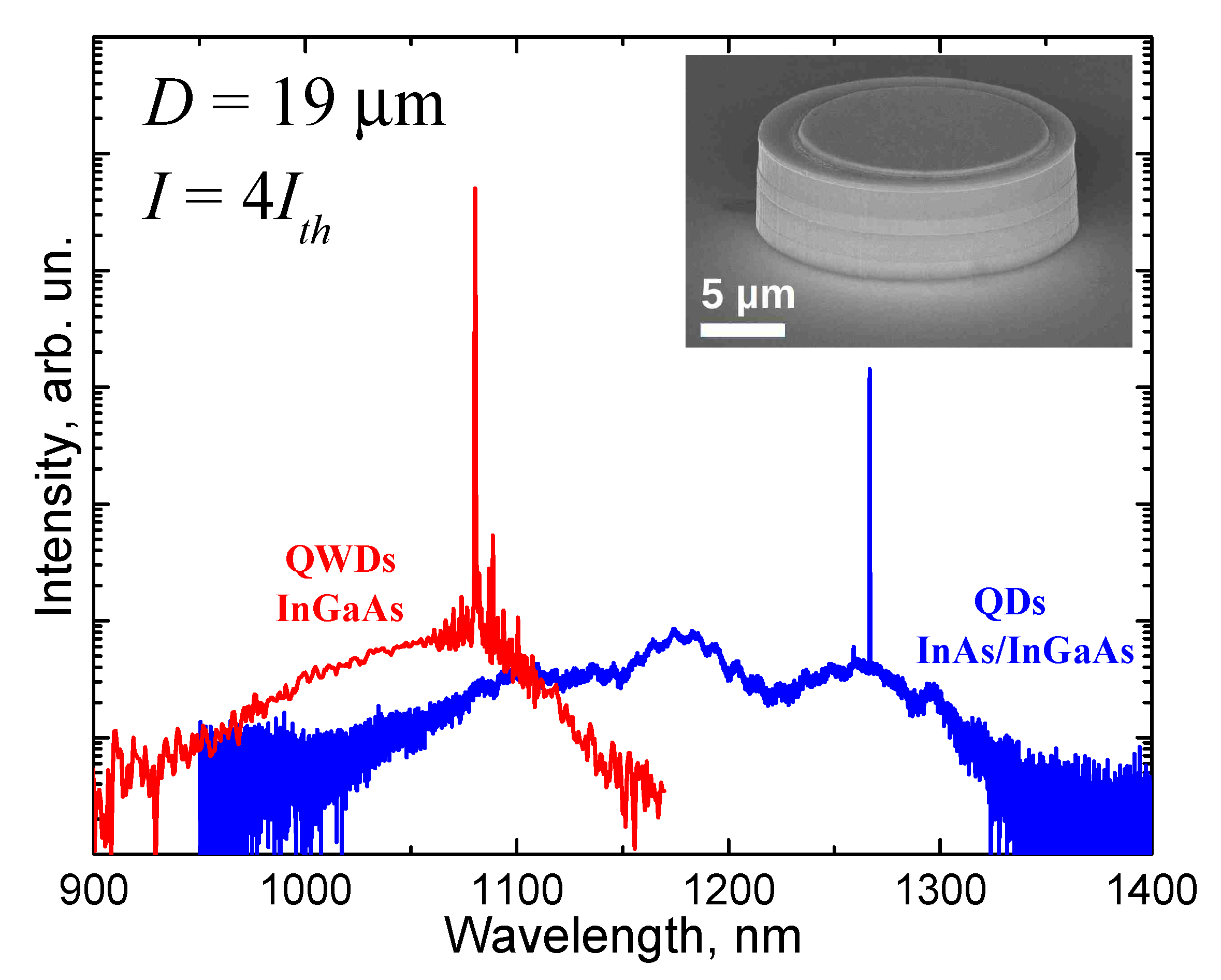
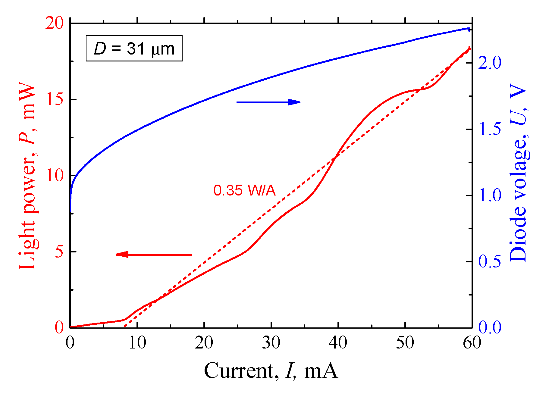
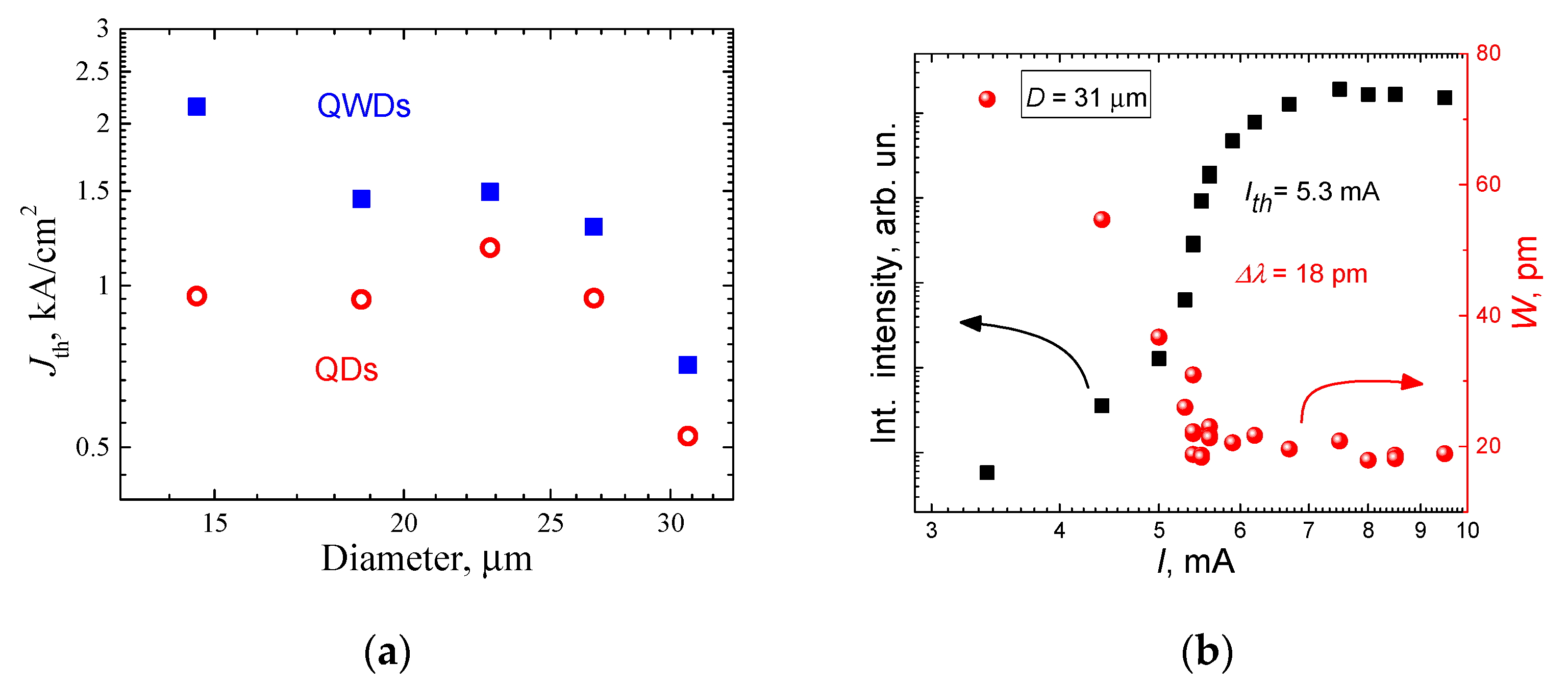
3.5.1. CW Performance

Recently semiconductor microlasers have attracted considerable interest as ultrasmall light sources for photonic integrated circuits and other applications. To meet the requirements of high efficiency, the major part of the output power should be emitted via lasing whispering gallery modes (WGMs), whereas the spontaneous emission should be weak. Although ideal microdisk (MD) can exhibit very high-quality factors [74], the non-ideal shape of actual devices results in an increase in optical loss [75], and thus, MD can emit practically sufficient optical power. For example, in [76], central electrically pumped 3 μm in radius microlaser with a single layer of InGaAs QDs as an active medium was employed for optical excitation of five closely spaced micropillar cavities. The out-coupling of the laser emission can be significantly enhanced through the use of optical fiber tapers. In reference [77] a laser differential efficiency as high as 16% and out-coupling efficiency in excess of 28% was measured in GaAs microdisk based on InAs QDs embedded in In0.15Ga0.85As quantum well after accounting for losses in the optical fiber system. Maximal power in the lasing line using free-space collection was estimated as 2.5 nW, whereas it was as high as 60 nW when using fiber taper collection. In reference [78] output power emitted into free space was directly measured for the first time in MD lasers based on InAs/InGaAs/GaAs QDs. The device was 31 μm in diameter, and its active region contained ten layers of InAs/InGaAs QDs in GaAs matrix. Total emitted optical power reached approximately 0.1 mW in CW regime, while the WGM emission amounted to about 2.8% of the total power.
In this section, we describe static characteristics of microdisk lasers based on QWDs [79].
The typical laser structure consisted of p- and n-type doped Al0.34Ga0.66As cladding layers and a 0.8 μm-thick undoped GaAs waveguiding layer. An active region represents five sheets of QWDs separated with 40 nm-thick GaAs spacers. The QWDs were formed by the deposition of eight monolayers of In0.4Ga0.6As. Microdisks with diameters from 15 to 31 μm were fabricated by standard post-growth processing. A micrograph of a 31-μm microlaser is shown in the inset of Figure 16.
Figure 16 compares electroluminescence spectra for a 19 μm in diameter MD lasers based on InGaAs/GaAs QWDs and 1.3 μm InAs/InGaAs/GaAs self-organized QDs. Both spectra are measured at injection current four times exceeding the threshold value. In the emission spectrum of QD microlaser, there are many narrow lines corresponding to WGM modes of different orders superimposed to a 180 nm wide spontaneous emission spectrum with the well-resolved peaks from the ground state, first and second excited states. The integrated intensity of all lasing WGMs is 18% of the entire emitted power.
In contrast, in MDs with QWDs, the width of the spontaneous emission spectrum is much lower (~70 nm). The peaks due to the excited-state transitions do not emerge up to very high injection currents. For the QWD MD laser, the share of the lasing WGM to the total emitted power is 95%. The lasing mode peak intensity is 29.9 dB higher as compared to that of the side (next brightest) mode.
At 60 mA, the total output power emitted into free space reaches 18.5 mW that corresponds to a wall-plug efficiency of about 15% (Figure 17). The share of all lasing WGMs in the total emitted power is 96%, whereas the fraction of dominating WGM at 1086 nm is about 75%.
Figure 18 compares the dependencies of threshold current density on mesa diameter for MD lasers based on InGaAs/GaAs QWDs and 1.3 μm InAs/InGaAs/GaAs self-organized QDs. The threshold was determined from the light-current characteristic showing a pronounced knee accompanied by linewidth narrowing down to 18 ± 2 pm (our spectral resolution limit). A representative dependence of the dominant mode intensity and linewidth on injection current for a 31 μm in diameter QWD MD laser is shown in Figure 18b.
When QWD MD diameter decreases from 31 μm to 15 μm threshold current density grows from 710 A cm−2 up to 2300 A cm−2 (Figure 18a). Such a sufficiently steep threshold current increase can be explained by the fact that the relative contribution of non-radiative recombination at MD sidewalls into total threshold current increases with a decrease in MD diameter. In MD lasers based on 1.3 μm InAs/InGaAs/GaAs QDs threshold current density is nearly independent of MD diameters in the range of 14–31 μm. These facts are in agreement with the results of mesa arrays studies (Section 3.2), showing that carrier lateral diffusion lengths in QDs are shorter than in QWDs.
In 31 μm in diameter, QWD MD lasing was observed up to 110 °C, and the maximal temperature was restricted by the available equipment. For 19 μm in diameter MD laser, the maximal lasing temperature was 90 °C, whereas for 10.5 μm in diameter device it was only 40 °C. The smaller is the MD size; the steeper is the growth of threshold current density with temperature increase. The population of the continuum states in QWDs increases with temperature, and a greater fraction of carriers can diffuse towards etched sidewalls and experience non-radiative recombination. Thus, the component of the total threshold current, which corresponds to surface non-radiative recombination, rises with a decrease in MD size. We expect that passivation of MD sidewalls [80] will allow achieving low threshold high temperature lasing in QWD MD with diameters down to 10 μm

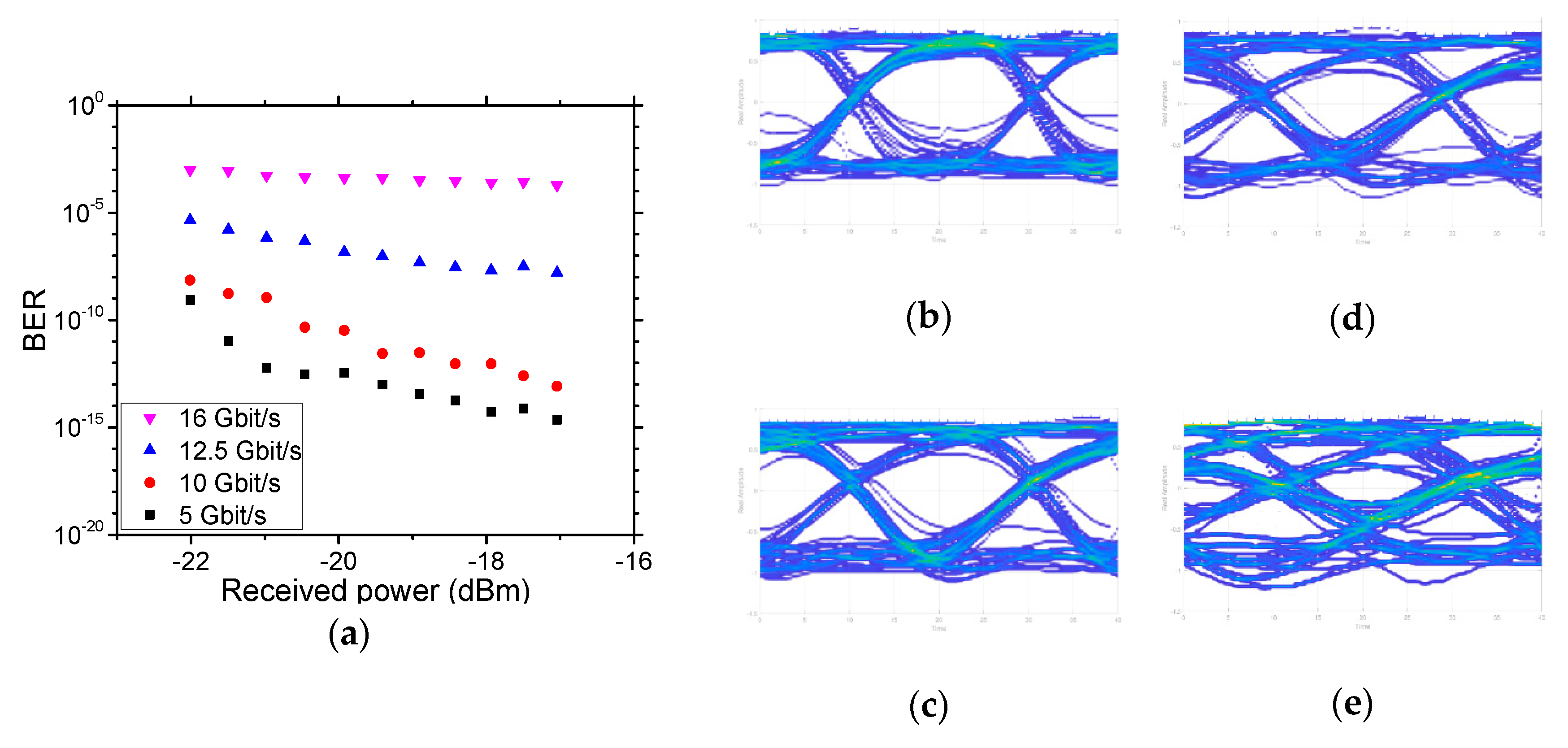
3.5.2. Dynamic Characteristics and Data Transmission

Presently main anticipated application of MD lasers is associated with ultrasmall light sources for optical data transmission between individual optical circuits and inside one circuit. Such an application requires efficient high-frequency modulation. Significant progress has been made in the development of InP-based microlasers based on QWs. A 7.5 μm in diameter circular MD laser bonded onto a silicon-on-insulator waveguide showed the 3-dB bandwidth of 3.5 GHz [81]. High-speed direct-modulation with a 3-dB bandwidth of 11.7 GHz and open eye diagrams at 10 Gbit/s were demonstrated for a 1550 nm InGaAsP/InP QW microdisk with a diameter of 7.5 μm bonded to silicon [82]. Small signal modulation (SSM) with a resonance frequency (fR) of 12.5 GHz was realized for an AlGaInAs/InP circular microlaser with a radius of 10 μm at 290 K. Furthermore, fR = 6.9 GHz, as well as clear eye diagrams at 12.5 Gbit/s, were observed for a 15-μm radius circular AlGaInAs/InP microlaser with active region based on six compressively strained QWs [83]. SSM with a 3-dB bandwidth exceeding 10 GHz was realized for a 30 μm microspiral AlGaInAs/InP disk based on eight QWs [84]. An open eye diagram at 15 Gbit/s with a bias current of 90 mA at a stage temperature of 15 °C was demonstrated [84]. More recently SSM response with 3-dB bandwidth up to 20 GHz was demonstrated for the AlGaInAs/InP microdisk laser with active region based on 6 QWs with a radius of 7 μm surrounded by BCB-cladding layer [85]. Eye diagrams at the bit rates of 20, 25, and 30 Gbit/s were also measured at the temperature of 14 °C [85].
In addition to applications in optical integrated circuits, MD lasers may become a cost-effective alternative for sophisticated and expensive distributed feedback lasers and vertical cavity surface-emitting laser for data transmission over intermediate and short distances. MD lasers have the inherent structural advantage of avoidance any kind of reflector either in the form of a cleaved facet or a diffraction grating. In paper [86] the authors report on the properties of directly modulated active-passive integrated 1570 nm InP-based microring lasers with an active region comprising six InGaAs QWs fabricated using full wafer bonding techniques. Bit rates up to 7 Gb/s were achieved for a 50 km singlemode fiber transmission.
The disadvantage of InP-based microlasers is caused by small energy offsets and low thermal conductivity [87], which results in a significant deterioration of their characteristics with temperature increase. For instance, in reference [85], it was observed that when the temperature rises from 14 to 40 °C, the resonance frequency value drops from 14.9 to about 8.3 GHz. However, dynamic characteristics of much more temperature stable GaAs-based MD lasers are poorly studied. 1 Gbit/s data transmission has been realized using a 6.5 μm in diameter MD laser based on In0.5Ga0.5As QDs [88].
It should be mentioned that in data transmission experiments by using InP-based microlasers, spectral filtering, and amplification of the lasing emission was utilized. The use of optical filters and amplifiers in photonic integrated circuit is obviously not desirable as it significantly increases the number of elements and fabrication complexity.
In this section, we describe the results on small-signal modulation and data transmission by MD lasers based on QWDs. These experiments were carried out without amplification of the lasing emission. Moreover, the microlasers were neither externally cooled nor temperature stabilized.
The microdisk design used for small signal modulation and data transmission experiment was the same as described in the previous section, but the planarizing layer was used. For high-frequency experiments, a ground-signal-ground (GSG) radio-frequency probe was used. All measurements were carried out at 300 K.
The 3-dB bandwidth (f3dB) is shown versus bias current in Figure 19. Examples of the SSM responses are depicted in the inset to this figure. The maximal f3dB of 6.7 GHz was obtained for the 23 μm in diameter microlaser at a bias current of 21 mA. The roll-over of the 3-dB bandwidth at high currents is attributed to the self-heating of the device.
To study the large signal modulation characteristics, the MD laser emission was coupled to the lensed fiber. Note that only 2.5% (32 μW at 25 mA) of the entire MD output power was fed into the fiber. Certain arrangements were undertaken to overcome the effects due to the photodetector noise and to measure the true dynamic performance of the MD lasers [89]. To obtain the eye diagrams, ten 27–1 pseudo-random bit sequences (PRBSs) were transmitted through the fiber. Figure 20b–e shows the eye diagrams at 30 °C ambient temperature for the optimum pumping regime. The received power was −15 dBm. The eye stays open up to bitrate Bmax = 12.5 Gbit/s. This result is in good agreement with the obtained maximal 3-dB bandwidth f3dB, max = 6.7 GHz (Figure 19) that suggests the estimation of Bmax ≈ 2f3dB, max = 13.4 Gbit/s. The dependence of bit error rate (BER) on the received optical power at 30°C is depicted in Figure 20a. Thus, the QWD MD lasers are applicable for 10 Gbit/s error-free data transmission (BER = 10−12). In case the output power of the QWD MD laser is increased by for instance, coupling to a bus ridge waveguide, e.g., like in Ref. [84], the data transmission speed can be further enhanced.

4. Conclusions

To conclude, quantum well-dots offer some advantages of both quantum wells and quantum dots and do show a combination of unique properties, such as high optical gain, the possibility of stacking a large number of layers in the active region, suppressed lateral transport of charge carriers, good temperature stability, applicability in the micro-resonators. In addition to previously achieved improvement of the performance of light converters, this allowed demonstrating high-performance edge-emitting lasers and microdisk lasers capable of error-free 10 Gbit/s data transmission at 30 °C without using an external optical amplifier and temperature stabilization. We expect that QWDs will found further applications in various optoelectronic devices where high optical gain and a large number of active layers are required, for instance, in vertical-cavity surface-emitting lasers, optical amplifiers, super-luminescent light-emitting diodes. Small carrier diffusion lengths are advantages for compact photonic devices where etching is done through the active area. Suppressed carrier lateral transport can reduce non-radiative recombination at facets of high-power lasers and thus decrease catastrophic optical mirror damage.

Author Contributions

Conceptualization, M.V.M. and A.E.Z.; growth-related part, S.A.M. and N.A.K.; microscopy, V.N.N. and S.S.R.; optical properties and visualization, A.M.N.; edge-emitting lasers, N.Y.G., Y.M.S. and A.S.P.; microdisk lasers, N.V.K. and E.I.M.; data transmission and high frequency analysis, A.E.Z. and F.I.Z. All authors have read and agreed to the published version of the manuscript.

Funding

This research was funded by the Russian Science Foundation (Grant № 16-12-10269).

Conflicts of Interest

The authors declare no conflict of interest.

References

  1. Bimberg, D.; Grundmann, M.; Ledentsov, N.N. Quantum Dot Heterostructures; Wiley: Hoboken, NJ, USA, 1999; ISBN 978-0-471-97388-1. [Google Scholar]
  2. Michler, P.; Kiraz, A.; Zhang, L.; Becher, C.; Hu, E.; Imamoglu, A. Laser emission from quantum dots in microdisk structures. Appl. Phys. Lett. 2000, 77, 184–186. [Google Scholar] [CrossRef] [Green Version]
  3. Reitzenstein, S.; Bazhenov, A.; Gorbunov, A.; Hofmann, C.; Münch, S.; Löffler, A.; Kamp, M.; Reithmaier, J.P.; Kulakovskii, V.D.; Forchel, A. Lasing in high-Q quantum-dot micropillar cavities. Appl. Phys. Lett. 2006, 89, 051107. [Google Scholar] [CrossRef]
  4. Chu, D.Y.; Chin, M.K.; Sauer, N.J.; Xu, Z.; Chang, T.Y.; Ho, S.T. 1.5-mu m InGaAs/InAlGaAs quantum-well microdisk lasers. IEEE Photonics Technol. Lett. 1993, 5, 1353–1355. [Google Scholar] [CrossRef]
  5. Luque, A.; Martí, A. Increasing the Efficiency of Ideal Solar Cells by Photon Induced Transitions at Intermediate Levels. Phys. Rev. Lett. 1997, 78, 5014–5017. [Google Scholar] [CrossRef]
  6. Kailuweit, P.; Kellenbenz, R.; Philipps, S.P.; Guter, W.; Bett, A.W.; Dimroth, F. Numerical simulation and modeling of GaAs quantum-well solar cells. J. Appl. Phys. 2010, 107, 064317. [Google Scholar] [CrossRef]
  7. Toprasertpong, K.; Fujii, H.; Thomas, T.; Führer, M.; Alonso-Álvarez, D.; Farrell, D.J.; Watanabe, K.; Okada, Y.; Ekins-Daukes, N.J.; Sugiyama, M.; et al. Absorption threshold extended to 1.15 eV using InGaAs/GaAsP quantum wells for over-50%-efficient lattice-matched quad-junction solar cells. Prog. Photovolt. Res. Appl. 2016, 24, 533–542. [Google Scholar] [CrossRef] [Green Version]
  8. Ho, W.-J.; Lee, Y.-Y.; Yang, G.-C.; Chang, C.-M. Optical and electrical characteristics of high-efficiency InGaP/InGaAs/Ge triple-junction solar cell incorporated with InGaAs/GaAs QD layers in the middle cell. Prog. Photovolt. Res. Appl. 2016, 24, 551–559. [Google Scholar] [CrossRef]
  9. Herz, L.M.; Phillips, R.T. Fine lines from dots. Nat. Mater. 2002, 1, 212–213. [Google Scholar] [CrossRef]
  10. Shchukin, V.A.; Ledentsov, N.N.; Bimberg, D. Epitaxy of Nanostructures; NanoScience and Technology; Springer: Berlin/Heidelberg, Germany, 2004; ISBN 978-3-642-08735-6. [Google Scholar]
  11. Griffin, P.R.; Barnes, J.; Barnham, K.W.J.; Haarpaintner, G.; Mazzer, M.; Zanotti-Fregonara, C.; Grünbaum, E.; Olson, C.; Rohr, C.; David, J.P.R.; et al. Effect of strain relaxation on forward bias dark currents in GaAs/InGaAs multiquantum well p–i–n diodes. J. Appl. Phys. 1996, 80, 5815–5820. [Google Scholar] [CrossRef]
  12. Wu, Q.; Grober, R.D.; Gammon, D.; Katzer, D.S. Excitons, biexcitons, and electron-hole plasma in a narrow 2.8-nm GaAs/AlxGa1−xAs quantum well. Phys. Rev. B 2000, 62, 13022–13027. [Google Scholar] [CrossRef]
  13. Gammon, D.; Snow, E.S.; Katzer, D.S. Excited state spectroscopy of excitons in single quantum dots. Appl. Phys. Lett. 1995, 67, 2391–2393. [Google Scholar] [CrossRef]
  14. Micallef, J.; Li, E.H.; Weiss, B.L. The effects of strain on the confinement profile of disordered InGaAs/GaAs single quantum wells. Superlattices Microstruct. 1993, 13, 125–132. [Google Scholar] [CrossRef]
  15. Unsleber, S.; Deppisch, M.; Krammel, C.M.; Vo, M.; Yerino, C.D.; Simmonds, P.J.; Lee, M.L.; Koenraad, P.M.; Schneider, C.; Höfling, S. Bulk AlInAs on InP(111) as a novel material system for pure single photon emission. Opt. Express 2016, 24, 23198–23206. [Google Scholar] [CrossRef] [Green Version]
  16. Martini, S.; Quivy, A.; Ugarte, D.; Lange, C.; Richter, W.; Tokranov, V. Step bunching in InGaAs/GaAs quantum wells grown by molecular beam epitaxy on GaAs(001) vicinal surfaces. J. Cryst. Growth 2001, 227–228, 46–50. [Google Scholar] [CrossRef]
  17. De Sales, F.V.; Soler, M.A.G.; Ugarte, D.; Quivy, A.A.; Da Silva, S.W.; Martini, S.; Morais, P.C. Step-Bunching Evidence in Strained InxGa1−xAs/GaAs Quantum Wells Grown on Vicinal (001) Substrates. Phys. Status Solidi Appl. Res. 2001, 187, 253–256. [Google Scholar] [CrossRef]
  18. Dong, H.; Sun, J.; Ma, S.; Liang, J.; Lu, T.; Liu, X.; Xu, B. Influence of substrate misorientation on the photoluminescence and structural properties of InGaAs/GaAsP multiple quantum wells. Nanoscale 2016, 8, 6043–6056. [Google Scholar] [CrossRef]
  19. Fujii, H.; Watanabe, K.; Nakano, Y.; Sodabanlu, H.; Sugiyama, M.; Toprasertpong, K.; Katoh, T. Thickness-modulated InGaAs/GaAsP superlattice solar cells on vicinal substrates. J. Appl. Phys. 2015, 117, 154501. [Google Scholar] [CrossRef]
  20. Alonso-Álvarez, D.; Thomas, T.; Führer, M.; Hylton, N.P.; Ekins-Daukes, N.J.; Lackner, D.; Philipps, S.P.; Bett, A.W.; Sodabanlu, H.; Fujii, H.; et al. InGaAs/GaAsP strain balanced multi-quantum wires grown on misoriented GaAs substrates for high efficiency solar cells. Appl. Phys. Lett. 2014, 105, 083124. [Google Scholar] [CrossRef] [Green Version]
  21. Poser, F.; Bhattacharya, A.; Weeke, S.; Richter, W. Growth of spatially ordered InAs quantum dots on step-bunched vicinal GaAs (1 0 0) substrates. J. Cryst. Growth 2003, 248, 317–321. [Google Scholar] [CrossRef]
  22. Lee, S.; Akabori, M.; Shirahata, T.; Takada, K.; Motohisa, J.; Fukui, T. The initial stage of InGaAs growth by MOVPE on multiatomic-stepped GaAs structures. J. Cryst. Growth 2001, 231, 75–81. [Google Scholar] [CrossRef]
  23. alhuda Al Saqri, N.; Felix, J.F.; Aziz, M.; Kunets, V.P.; Jameel, D.; Taylor, D.; Henini, M.; Abd El-sadek, M.S.; Furrow, C.; Ware, M.E.; et al. Investigation of electrically active defects in InGaAs quantum wire intermediate-band solar cells using deep-level transient spectroscopy technique. Nanotechnology 2017, 28, 045707. [Google Scholar] [CrossRef] [PubMed] [Green Version]
  24. Kunets, V.P.; Furrow, C.S.; Morgan, T.A.; Hirono, Y.; Ware, M.E.; Dorogan, V.G.; Mazur, Y.I.; Kunets, V.P.; Salamo, G.J. InGaAs quantum wire intermediate band solar cell. Appl. Phys. Lett. 2012, 101, 041106. [Google Scholar] [CrossRef]
  25. Sugiyama, M.; Fujii, H.; Katoh, T.; Toprasertpong, K.; Sodabanlu, H.; Watanabe, K.; Alonso-Álvarez, D.; Ekins-Daukes, N.J.; Nakano, Y. Quantum wire-on-well (WoW) cell with long carrier lifetime for efficient carrier transport. Prog. Photovolt. Res. Appl. 2016, 24, 1606–1614. [Google Scholar] [CrossRef] [Green Version]
  26. Cho, H.; Toprasertpong, K.; Sodabanlu, H.; Watanabe, K.; Sugiyama, M.; Nakano, Y. Stability and controllability of InGaAs/GaAsP wire-on-well (WoW) structure for multi-junction solar cells. J. Cryst. Growth 2017, 464, 86–93. [Google Scholar] [CrossRef]
  27. Yu, Q.; Li, X.; Jia, Y.; Lu, W.; Zheng, M.; Zhang, X.; Ning, Y.; Wu, J. InGaAs-Based Well-Island Composite Quantum-Confined Structure with Superwide and Uniform Gain Distribution for Great Enhancement of Semiconductor Laser Performance. ACS Photonics 2018, 5, 4896–4902. [Google Scholar] [CrossRef]
  28. Talalaev, V.G.; Novikov, B.V.; Verbin, S.Y.; Novikov, A.B.; Thath, D.S.; Shchur, I.V.; Gobsch, G.; Goldhahn, R.; Stein, N.; Golombek, A.; et al. Recombination emission from InAs quantum dots grown on vicinal GaAs surfaces. Semiconductors 2000, 34, 453–461. [Google Scholar] [CrossRef]
  29. Evtikhiev, V.P.; Tokranov, V.E.; Kryzhanovskii, A.K.; Boiko, A.M.; Suris, R.A.; Titkov, A.N.; Nakamura, A.; Ichida, M. Growth of InAs quantum dots on vicinal GaAs(001) surfaces misoriented in the [010] direction. Semiconductors 1998, 32, 765–769. [Google Scholar] [CrossRef]
  30. Yazdanpanah, V.; Wang, Z.M.; Lee, J.H.; Salamo, G.J. Structural evolution in strained In0.18Ga0.82As stacking multilayers on vicinal GaAs surfaces. New J. Phys. 2006, 8, 233. [Google Scholar] [CrossRef] [Green Version]
  31. Ledentsov, N.N.; Bimberg, D.; Shernyakov, Y.M.; Kochnev, V.; Maximov, M.V.; Sakharov, A.V.; Krestnikov, I.L.; Egorov, A.Y.; Zhukov, A.E.; Tsatsul’nikov, A.F.; et al. Properties of strained (In, Ga, Al)As lasers with laterally modulated active region. Appl. Phys. Lett. 1997, 70, 2888–2890. [Google Scholar] [CrossRef]
  32. Mintairov, S.A.; Kalyuzhnyy, N.A.; Maximov, M.V.; Nadtochiy, A.M.; Rouvimov, S.; Zhukov, A.E. GaAs quantum well-dots solar cells with spectral response extended to 1100 nm. Electron. Lett. 2015, 51, 1602–1604. [Google Scholar] [CrossRef]
  33. Löffler, A.; Reithmaier, J.P.; Forchel, A.; Sauerwald, A.; Peskes, D.; Kümmell, T.; Bacher, G. Influence of the strain on the formation of GaInAs/GaAs quantum structures. J. Cryst. Growth 2006, 286, 6–10. [Google Scholar] [CrossRef]
  34. Hubbard, S.M.; Podell, A.; Mackos, C.; Polly, S.; Bailey, C.G.; Forbes, D.V. Effect of vicinal substrates on the growth and device performance of quantum dot solar cells. Sol. Energy Mater. Sol. Cells 2013, 108, 256–262. [Google Scholar] [CrossRef]
  35. Bhattacharya, A.; Mawst, L.J.; Nayak, S.; Li, J.; Kuech, T.F. Interface structures of InGaAs/InGaAsP/InGaP quantum well laser diodes grown by metalorganic chemical vapor deposition on GaAs substrates. Appl. Phys. Lett. 1996, 68, 2240–2242. [Google Scholar] [CrossRef]
  36. Nadtochiy, A.M.; Maximov, M.V.; Mintairov, S.A.; Kalyuzhnyy, N.A.; Nevedomskiy, V.N.; Rouvimov, S.S.; Zhukov, A.E. Gradual Evolution From Quantum-Well-Like to Quantum-Dot-Like Characteristics in InGaAs/GaAs Nanostructures. Phys. Status Solidi 2018, 255, 1800123. [Google Scholar] [CrossRef]
  37. De Sales, F.V.; Soler, M.A.G.; Ugarte, D.; Abramof, E.; Quivy, A.A.; Da Silva, S.W.; Martini, S.; Morais, P.C.; Leite, J.R. Investigation of optical and structural properties of InxGa1−xAs/GaAs quantum wells grown on vicinal GaAs(0 0 1) substrates. Phys. B Condens. Matter 2002, 311, 285–291. [Google Scholar] [CrossRef]
  38. Strand, T.A.; Thibeault, B.J.; Coldren, L.A. Reduced lateral carrier diffusion for improved miniature semiconductor lasers. J. Appl. Phys. 1997, 81, 3377–3381. [Google Scholar] [CrossRef]
  39. Kim, J.K.; Naone, R.L.; Coldren, L.A. Lateral carrier confinement in miniature lasers using quantum dots. IEEE J. Sel. Top. Quantum Electron. 2000, 6, 504–510. [Google Scholar] [CrossRef]
  40. Naone, R.L.; Floyd, P.D.; Young, D.B.; Hegblom, E.R.; Strand, T.A.; Coldren, L.A. Interdiffused quantum wells for lateral carrier confinement in VCSELs. IEEE J. Sel. Top. Quantum Electron. 1998, 4, 706–714. [Google Scholar] [CrossRef]
  41. Gérard, J.M.; Cabrol, O.; Sermage, B. InAs quantum boxes: Highly efficient radiative traps for light emitting devices on Si. Appl. Phys. Lett. 1996, 68, 3123–3125. [Google Scholar] [CrossRef]
  42. Piva, P.G.; Goldberg, R.D.; Mitchell, I.V.; Labrie, D.; Leon, R.; Charbonneau, S.; Wasilewski, Z.R.; Fafard, S. Enhanced degradation resistance of quantum dot lasers to radiation damage. Appl. Phys. Lett. 2000, 77, 624–626. [Google Scholar] [CrossRef] [Green Version]
  43. Ribbat, C.; Sellin, R.; Grundmann, M.; Bimberg, D.; Sobolev, N.A.; Carmo, M.C. Enhanced radiation hardness of quantum dot lasers to high energy proton irradiation. Electron. Lett. 2001, 37, 174–175. [Google Scholar] [CrossRef]
  44. Arzberger, M.; Böhm, G.; Amann, M.-C.; Abstreiter, G. Continuous room-temperature operation of electrically pumped quantum-dot microcylinder lasers. Appl. Phys. Lett. 2001, 79, 1766–1768. [Google Scholar] [CrossRef]
  45. Luo, K.J.; Xu, J.Y.; Cao, H.; Ma, Y.; Chang, S.H.; Ho, S.T.; Solomon, G.S. Ultrafast dynamics of InAs/GaAs quantum-dot microdisk lasers. Appl. Phys. Lett. 2001, 78, 3397–3399. [Google Scholar] [CrossRef]
  46. Fiore, A.; Chen, J.X.; Ilegems, M. Scaling quantum-dot light-emitting diodes to submicrometer sizes. Appl. Phys. Lett. 2002, 81, 1756–1758. [Google Scholar] [CrossRef] [Green Version]
  47. Kryzhanovskaya, N.V.; Zhukov, A.E.; Maximov, M.V.; Moiseev, E.I.; Shostak, I.I.; Nadtochiy, A.M.; Kudashova, Y.V.; Lipovskii, A.A.; Kulagina, M.M.; Troshkov, S.I. Room Temperature Lasing in 1-μm Microdisk Quantum Dot Lasers. IEEE J. Sel. Top. Quantum Electron. 2015, 21, 709–713. [Google Scholar] [CrossRef]
  48. Zeng, K.C.; Lin, J.Y.; Jiang, H.X. Effects of alloy disorder on the transport properties of AlxGa1−xN epilayers probed by persistent photoconductivity. Appl. Phys. Lett. 2000, 76, 1728–1730. [Google Scholar] [CrossRef] [Green Version]
  49. Kurtz, S.R.; Klem, J.F.; Allerman, A.A.; Sieg, R.M.; Seager, C.H.; Jones, E.D. Minority carrier diffusion and defects in InGaAsN grown by molecular beam epitaxy. Appl. Phys. Lett. 2002, 80, 1379–1381. [Google Scholar] [CrossRef]
  50. Maximov, M.V.; Volovik, B.V.; Sotomayor Torres, C.M.; Ramushina, E.M.; Skopina, V.I.; Tanklevskaya, E.M.; Gurevich, S.A.; Ustinov, V.M.; Alferov, Z.I.; Ledentsov, N.N.; et al. Impact of Carrier Lateral Transport and Surface Recombination on the PL Efficiency of Mesas with Self-Organized Quantum Dots. Phys. Status Solidi 2001, 188, 955–959. [Google Scholar] [CrossRef]
  51. Maximov, M.V.; Tsatsul’nikov, A.F.; Volovik, B.V.; Sizov, D.S.; Shernyakov, Y.M.; Kaiander, I.N.; Zhukov, A.E.; Kovsh, A.R.; Mikhrin, S.S.; Ustinov, V.M.; et al. Tuning quantum dot properties by activated phase separation of an InGa(Al)As alloy grown on InAs stressors. Phys. Rev. B 2000, 62, 16671–16680. [Google Scholar] [CrossRef]
  52. Fiore, A.; Rossetti, M.; Alloing, B.; Paranthoen, C.; Chen, J.X.; Geelhaar, L.; Riechert, H. Carrier diffusion in low-dimensional semiconductors: A comparison of quantum wells, disordered quantum wells, and quantum dots. Phys. Rev. B 2004, 70, 205311. [Google Scholar] [CrossRef] [Green Version]
  53. Nadtochiy, A.M.; Mintairov, S.A.; Kalyuzhnyy, N.A.; Maximov, M.V.; Sannikov, D.A.; Yagafarov, T.F.; Zhukov, A.E. Time-Resolved Photoluminescence of InGaAs Nanostructures Different in Quantum Dimensionality. Semiconductors 2019, 53, 1489–1495. [Google Scholar] [CrossRef]
  54. Heitz, R.; Born, H.; Lüttgert, T.; Hoffmann, A.; Bimberg, D. Resonantly Excited Time-Resolved Photoluminescence Study of Self-Organized InGaAs/GaAs Quantum Dots. Phys. Status Solidi 2000, 221, 65–70. [Google Scholar] [CrossRef]
  55. Markus, A.; Fiore, A.; Ganière, J.D.; Oesterle, U.; Chen, J.X.; Deveaud, B.; Ilegems, M.; Riechert, H. Comparison of radiative properties of InAs quantum dots and GaInNAs quantum wells emitting around 1.3 μm. Appl. Phys. Lett. 2002, 80, 911–913. [Google Scholar] [CrossRef] [Green Version]
  56. Nasr, O.; Chauvin, N.; Alouane, M.H.H.; Maaref, H.; Bru-Chevallier, C.; Sfaxi, L.; Ilahi, B. Carrier dynamics of strain-engineered InAs quantum dots with (In)GaAs surrounding material. J. Opt. 2017, 19, 025401. [Google Scholar] [CrossRef]
  57. Karachinsky, L.Y.; Pellegrini, S.; Buller, G.S.; Shkolnik, A.S.; Gordeev, N.Y.; Evtikhiev, V.P.; Novikov, V.B. Time-resolved photoluminescence measurements of InAs self-assembled quantum dots grown on misorientated substrates. Appl. Phys. Lett. 2004, 84, 7–9. [Google Scholar] [CrossRef] [Green Version]
  58. Pellegrini, S.; Buller, G.S.; Karachinsky, L.Y.; Shkolnik, A.S.; Gordeev, N.Y.; Zegrya, G.G.; Evtikhiev, V.P.; Sellers, I.R.; Skolnick, M.S.; Liu, H.Y.; et al. Time-resolved photoluminescence measurements of InAs self-assembled quantum dots (Invited Paper). In Proceedings of the Ultrafast Phenomena in Semiconductors and Nanostructure Materials IX, San Francisco, CA, USA, 20 April 2011. [Google Scholar]
  59. Gurioli, M.; Vinattieri, A.; Colocci, M.; Deparis, C.; Massies, J.; Neu, G.; Bosacchi, A.; Franchi, S. Temperature dependence of the radiative and nonradiative recombination time in GaAs/AlxGa1−xAs quantum-well structures. Phys. Rev. B 1991, 44, 3115–3124. [Google Scholar] [CrossRef]
  60. Maximov, M.V.; Zhukov, A.E. Quantum Dot Lasers. In Dekker Encyclopedia of Nanoscience and Nanotechnology; CRC: Boca Raton, FL, USA, 2014. [Google Scholar]
  61. Browne, B.; Lacey, J.; Tibbits, T.; Bacchin, G.; Wu, T.-C.; Liu, J.Q.; Chen, X.; Rees, V.; Tsai, J.; Werthen, J.-G. Triple-junction quantum-well solar cells in commercial production. In Proceedings of the AIP Conference Proceedings, Tallahassee, FL, USA, 1–2 August 2012; pp. 3–5. [Google Scholar] [CrossRef] [Green Version]
  62. Fujii, H.; Toprasertpong, K.; Wang, Y.; Watanabe, K.; Sugiyama, M.; Nakano, Y. 100-period, 1.23-eV bandgap InGaAs/GaAsP quantum wells for high-efficiency GaAs solar cells: Toward current-matched Ge-based tandem cells. Prog. Photovolt. Res. Appl. 2014, 22, 784–795. [Google Scholar] [CrossRef]
  63. Bailey, C.G.; Forbes, D.V.; Polly, S.J.; Bittner, Z.S.; Dai, Y.; Mackos, C.; Raffaelle, R.P.; Hubbard, S.M. Open-Circuit Voltage Improvement of InAs/GaAs Quantum-Dot Solar Cells Using Reduced InAs Coverage. IEEE J. Photovolt. 2012, 2, 269–275. [Google Scholar] [CrossRef]
  64. Forbes, D.V.; Hubbard, S.M.; Bailey, C.; Polly, S.; Andersen, J.; Raffaelle, R. III-V Quantum Dot Enhanced Photovoltaic Devices. In Proceedings of the Next Generation (Nano) Photonic and Cell Technologies for Solar Energy Conversion, San Diego, CA, USA, 1–5 August 2010; Tsakalakos, L., Ed.; p. 77720C. [Google Scholar] [CrossRef]
  65. Kalyuzhnyy, N.A.; Mintairov, S.A.; Salii, R.A.; Nadtochiy, A.M.; Payusov, A.S.; Brunkov, P.N.; Nevedomsky, V.N.; Shvarts, M.Z.; Martí, A.; Andreev, V.M.; et al. Increasing the quantum efficiency of InAs/GaAs QD arrays for solar cells grown by MOVPE without using strain-balance technology. Prog. Photovolt. Res. Appl. 2016, 24. [Google Scholar] [CrossRef] [Green Version]
  66. Weber, H.; Loosen, P.; Poprawe, R. (Eds.) Landolt-Börnstein—Group VIII Advanced Materials and Tec hnologies. In Laser Systems; Springer: Berlin/Heidelberg, Germany, 2011; Volume 3, ISBN 978-3-642-14176-8. [Google Scholar]
  67. Zhukov, A.E.; Maksimov, M.V.; Kovsh, A.R. Device characteristics of long-wavelength lasers based on self-organized quantum dots. Semiconductors 2012, 46, 1225–1250. [Google Scholar] [CrossRef]
  68. Adams, A.R. Strained-Layer Quantum-Well Lasers. IEEE J. Sel. Top. Quantum Electron. 2011, 17, 1364–1373. [Google Scholar] [CrossRef]
  69. Serin, A.A.; Payusov, A.S.; Shernyakov, Y.M.; Kalyuzhnyy, N.A.; Mintairov, S.A.; Maximov, M.V.; Gordeev, N.Y.; Zhukov, A.E. Reducing of thermal resistance of edge-emitting lasers based on coupled waveguides. J. Phys. Conf. Ser. 2018, 1124, 041016. [Google Scholar] [CrossRef]
  70. Rauch, S.; Wenzel, H.; Radziunas, M.; Haas, M.; Tränkle, G.; Zimer, H. Impact of longitudinal refractive index change on the near-field width of high-power broad-area diode lasers. Appl. Phys. Lett. 2017, 110, 263504. [Google Scholar] [CrossRef]
  71. Nadtochiy, A.M.; Maximov, M.V.; Rouvimov, S.S.; Zhukov, A.E.; Shernyakov, Y.M.; Payusov, A.S.; Kalyuzhnyy, N.A.; Mintairov, S.A. Effect of the bimodality of a QD array on the optical properties and threshold characteristics of QD lasers. Semiconductors 2015, 49, 1090–1094. [Google Scholar] [CrossRef]
  72. Gordeev, N.Y.; Payusov, A.S.; Shernyakov, Y.M.; Mintairov, S.A.; Kalyuzhnyy, N.A.; Kulagina, M.M.; Maximov, M.V. Transverse single-mode edge-emitting lasers based on coupled waveguides. Opt. Lett. 2015, 40, 2150–2152. [Google Scholar] [CrossRef]
  73. Pietrzak, A.; Zorn, M.; Huelsewede, R.; Meusel, J.; Sebastian, J. Development of highly-efficient laser diodes emitting around 1060nm for medical and industrial applications. In Proceedings of the High-Power Diode Laser Technology XVII, San Francisco, CA, USA, 2–7 February 2019; Zediker, M.S., Ed.; p. 17. [Google Scholar] [CrossRef]
  74. McCall, S.L.; Levi, A.F.J.; Slusher, R.E.; Pearton, S.J.; Logan, R.A. Whispering-gallery mode microdisk lasers. Appl. Phys. Lett. 1992, 60, 289–291. [Google Scholar] [CrossRef]
  75. Borselli, M.; Johnson, T.J.; Painter, O. Beyond the Rayleigh scattering limit in high-Q silicon microdisks: Theory and experiment. Opt. Express 2005, 13, 1515–1530. [Google Scholar] [CrossRef] [Green Version]
  76. Stock, E.; Albert, F.; Hopfmann, C.; Lermer, M.; Schneider, C.; Höfling, S.; Forchel, A.; Kamp, M.; Reitzenstein, S. On-Chip Quantum Optics with Quantum Dot Microcavities. Adv. Mater. 2013, 25, 707–710. [Google Scholar] [CrossRef]
  77. Srinivasan, K.; Borselli, M.; Painter, O.; Stintz, A.; Krishna, S. Cavity Q, mode volume, and lasing threshold in small diameter AlGaAs microdisks with embedded quantum dots. Opt. Express 2006, 14, 1094–1105. [Google Scholar] [CrossRef] [Green Version]
  78. Zubov, F.I.; Kryzhanovskaya, N.V.; Moiseev, E.I.; Polubavkina, Y.S.; Simchuk, O.I.; Kulagina, M.M.; Zadiranov, Y.M.; Troshkov, S.I.; Lipovskii, A.A.; Maximov, M.V.; et al. Laser characteristics of an injection microdisk with quantum dots and its free-space outcoupling efficiency. Semiconductors 2016, 50, 1408–1411. [Google Scholar] [CrossRef]
  79. Moiseev, E.; Kryzhanovskaya, N.; Maximov, M.; Zubov, F.; Nadtochiy, A.; Kulagina, M.; Zadiranov, Y.; Kalyuzhnyy, N.; Mintairov, S.; Zhukov, A. Highly efficient injection microdisk lasers based on quantum well-dots. Opt. Lett. 2018, 43, 4554–4557. [Google Scholar] [CrossRef] [PubMed]
  80. Kryzhanovskaya, N.V.; Lebedev, M.V.; L’vova, T.V.; Kudashova, Y.V.; Shostak, I.I.; Moiseev, E.I.; Zhukov, A.E.; Maximov, M.V.; Kulagina, M.M.; Nadtochiy, A.M.; et al. The effect of sulfide passivation on luminescence from microdisks with quantum wells and quantum dots. Tech. Phys. Lett. 2015, 41, 654–657. [Google Scholar] [CrossRef]
  81. Liu, L.; Roelkens, G.; Van Campenhout, J.; Brouckaert, J.; Van Thourhout, D.; Baets, R. III–V/Silicon-on-Insulator Nanophotonic Cavities for Optical Network-on-Chip. J. Nanosci. Nanotechnol. 2010, 10, 1461–1472. [Google Scholar] [CrossRef] [PubMed] [Green Version]
  82. Hofrichter, J.; Raz, O.; Keyvaninia, S.; de Vries, T.; Dorren, H.J.S.; Morf, T.; Offrein, B.J. High-Speed Direct-Modulation of InP Microdisk Lasers. In Proceedings of the 39th European Conference and Exhibition on Optical Communication (ECOC 2013), London, UK, 22–26 September 2013; pp. 351–353. [Google Scholar] [CrossRef]
  83. Lv, X.-M.; Huang, Y.-Z.; Zou, L.-X.; Long, H.; Du, Y. Optimization of direct modulation rate for circular microlasers by adjusting mode Q factor. Laser Photon. Rev. 2013, 7, 818–829. [Google Scholar] [CrossRef]
  84. Yang, Y.-D.; Zhang, Y.; Huang, Y.-Z.; Poon, A.W. Direct-modulated waveguide-coupled microspiral disk lasers with spatially selective injection for on-chip optical interconnects. Opt. Express 2014, 22, 824–838. [Google Scholar] [CrossRef]
  85. Zou, L.-X.; Huang, Y.-Z.; Liu, B.-W.; Lv, X.-M.; Ma, X.-W.; Yang, Y.-D.; Xiao, J.-L.; Du, Y. Thermal and high speed modulation characteristics for AlGaInAs/InP microdisk lasers. Opt. Express 2015, 23, 2879–2888. [Google Scholar] [CrossRef]
  86. Kapsalis, A.; Syvridis, D.; Troppenz, U.; Hamacher, M.; Heidrich, H. 7Gb/s Direct Modulation of Vertically Coupled Microring Lasers. In Proceedings of the Optical Fiber Communication Conference/National Fiber Optic Engineers Conference, San Diego, CA, USA, 24–28 February 2008. [Google Scholar]
  87. Sokół, A.K.; Sarzała, R.P. Comparative analysis of thermal problems in GaAs- and InP-based 1.3-μm VECSELs. Opt. Appl. 2013, 43, 325–341. [Google Scholar] [CrossRef]
  88. Mao, M.-H.; Chien, H.-C. Transient behaviors of current-injection quantum-dot microdisk lasers. Opt. Express 2012, 20, 3302–3310. [Google Scholar] [CrossRef]
  89. Zubov, F.; Maximov, M.; Kryzhanovskaya, N.; Moiseev, E.; Muretova, M.; Mozharov, A.; Kaluzhnyy, N.; Mintairov, S.; Kulagina, M.; Ledentsov, N.; et al. High speed data transmission using directly modulated microdisk lasers based on InGaAs/GaAs quantum well-dots. Opt. Lett. 2019, 44, 5442–5445. [Google Scholar] [CrossRef]
Figure 1. Schematic representation of InGaAs structures of different dimensionalities—self-organized Stranski–Krastanow quantum dots, QDs (a); quantum well-dots, QWDs (b); and quantum wells, QW (c).
Applsci 10 01038 g001
Figure 2. Plan-view (001) TEM images of the samples of the InxGa1−xAs QWD layers with nominal indium composition x = 0.3 (a), 0.4 (b), and 0.5 (c) (effective vector of diffraction g = (220)). Insets show a cross-section of images of the same samples in the [1–10] zone.
Applsci 10 01038 g002
Figure 3. Cross-section of images in the [1–10] zone of the In0.4Ga0.6As QWD layers grown on (a) vicinal and (b) exact-oriented GaAs substrates.
Applsci 10 01038 g003aApplsci 10 01038 g003b
Figure 4. Cross-section images in the [1–10] zone of the 15 stacked In0.4Ga0.6As QWD layers.
Applsci 10 01038 g004
Figure 5. Schematic representation of temperature-dependent evolution of QWD PL spectra: low (a), moderate (b), and elevated (c) temperatures.
Applsci 10 01038 g005aApplsci 10 01038 g005b
Figure 6. PL spectra of InGaAs QWDs with 30%, 40%, and 50% In composition measured in the conditions of random carrier population—20 K (a), one-way carrier transport—100 K (b) and equilibrium (Fermi) carrier distribution—300 K (c) in joint QWD/QD array.
Applsci 10 01038 g006
Figure 7. Evolution of the PL spectra of the QWDs with the increase in the nominal thickness of the deposited InGaAs from 7 ML to 10 ML, taken at 100 K.
Applsci 10 01038 g007
Figure 8. PL intensity mesas with QDs, QWDs, and QWs as a function of mesa diameter measured at 77 K (a) and 290 K (b). Insets: microscopic images of mesa arrays taken with different magnification.
Applsci 10 01038 g008
Figure 9. Normalized PL spectra (a) and temporal evolution of PL signal at its spectral maximum (b) for quantum dots (blue), quantum well-dots (green), and quantum well (red).
Applsci 10 01038 g009
Figure 10. The dependencies of laser characteristics on stripe length for devices with different number of QWD layers: (a) lasing wavelength, (b) threshold current density, and (c) inverse differential efficiency.
Applsci 10 01038 g010
Figure 11. Below-threshold electroluminescence (a) and lasing (b) spectra of the lasers with different numbers of QWD layers.
Applsci 10 01038 g011
Figure 12. The dependences of modal gain on the injection current density for devices with different numbers of QWD layers.
Applsci 10 01038 g012
Figure 13. Temperature dependence of the threshold current of QWD-based laser.
Applsci 10 01038 g013
Figure 14. Dependencies of integral electroluminescence intensity on the current density for lasers based on (a) 1 QWD layer, and (b) 10 QWD layers.
Applsci 10 01038 g014
Figure 15. Dependencies of CW output power (left axis), voltage (right red axis), and power conversion efficiency (right blue axis) at room temperature on injected current for an edge-emitting laser based on 2 QWD layers (a); dependence of pulsed output power on injected current. Insets: spectra at two different currents (b).
Applsci 10 01038 g015
Figure 16. Lasing spectra of microdisk lasers based on (red) QWD and (blue) QD active area. The inset shows a microphotograph of the measured device.
Applsci 10 01038 g016
Figure 17. Total power in free space and voltage of a 31 μm in diameter MD laser as a function of current. Dotted line: 0.35 mW/mA.
Applsci 10 01038 g017
Figure 18. Threshold current of QWD (circles) and QD (squares) MD lasers as a function of diameter (a). Current dependence of integrated lasing line intensity (squares) and FWHM (circles) for the 1088 nm mode of a 31 μm MD laser (b).
Applsci 10 01038 g018
Figure 19. Dependence of 3-dB bandwidth (f3dB) on injection current. Inset: examples of small signal modulation responses at different bias currents. The line is a guide to the eye.
Applsci 10 01038 g019
Figure 20. The dependence of BER on the received optical power (a), and eye diagrams for 5 (b), 10 (c), 12.5 (d), and 16 (e) GHz for a 23 μm in diameter microdisk laser at 30 °C.
Applsci 10 01038 g020
Table 1. Comparison of the characteristics of quantum wells and quantum dots.
PropertiesInGaAs/GaAs QWsIn(Ga)As/GaAs QDs
Carrier localization2D0D
Maximal emission wavelength1100 nm 1350 nm
Optical gain/absorption per layer>20 cm−13–8 cm−1
Carrier lateral diffusion lengthSeveral microns~100 nm
Number of stacked layers (without strain compensation)3 (for λ ~ 1 μm)15–20 (for λ 1.1–1.3 μm)
Carrier capture time~ps or lessfew ps
Table 2. The characteristics of edge-emitting lasers based on a different number of QWD layers. The threshold current density and lasing wavelength are indicated for the cavity length 4 mm.
Number of QWD LayersThreshold Current Density, A/cm2Lasing Wavelength (λ), nmInternal Quantum Efficiency (ηi)Internal Loss (αi), cm−1
Total (jth)Per QWD Layer (jQWD)
110010010880.790.7
21206010920.851.0
52004011080.821.5
103753811170.782.4

