1. Introduction
Phase arrays have existed for more than a century. Their application in radar in the RF field plays an important role in beam forming and steering. In recent years, autonomous vehicle development has taken advantage of light detection and ranging (LiDAR) for higher spatial resolution. Traditional LiDAR utilizes the mechanical method, such as micro electro-mechanical systems (MEMS) mirrors, to steer the beam, but the inertia from a mechanical device limits the ability to reach a large steering angle and high speed at the same time. On the other hand, the optical phase array (OPA) shows no inertia phenomena, reaches large steering angles at high speed, and has the potential to be integrated into a small foot print.
The OPA was first developed on the silicon wire-based waveguide array through the optical splitter, phase manipulation, and emitter [
1,
2]. OPA through the thermal phase tuning for beam steering showed a lot of applications for solid state LiDAR, sensing, and imaging [
3,
4,
5]. Moreover, the unequally spaced waveguide array and different emitter waveguide widths were taken for a large steering angle [
6,
7]. For the 180-degree field of view with the grating lob-free beam formation, an index-mismatched waveguide on the emitter with the sub-wavelength pitch was demonstrated by a set of three widths, 300, 350, and 400-nm, in sequence [
8]. Since the previous three index-mismatched waveguides own different phases, a conventional approach is to implement addressable control for each emitter phase, which causes the complicated electronic circuit and total power consumption from the independent emitter elements.
In an OPA architecture, the input light can split into N outputs equally using a cascaded 1 × 2 multimode interference (MMI) coupler with n stages, where the relation between N and n is correlated with N = 2
n. In each stage, only half of the waveguides of each stage are embedded by phase shifters [
9]. Then, the accumulated phase shift on the N outputs will be 0, Δφ, 2Δφ, ……, (N−1)Δφ, respectively. Because the phase shifters on each stage provide the same phase shift, they can be driven by the same voltage. Here, we are using 64 emitters for demonstration. N and n are 64 and 6, respectively. Thus, the total number of voltages for controlling is six. Therefore, we can connect all phase shifters together with one input voltage with each stage, then the total phase shift is 192 Δφ (N(log
2N)/2, N = 64). In order to get an identical phase shift on each stage of N emitters through log
2N voltages, the phase difference from the index-mismatched waveguides needs to be matched.
The traditional method of calculating beam steering is phase array theory. The finite difference time domain (FDTD) is used to calculate the intensity distribution of a single antenna and then followed by the phase array theory. FDTD simulation is quite time consuming. In order to improve the computational efficiency on the LiDAR antenna, it is necessary to reduce the simulation time. Therefore, the Rayleigh–Sommerfeld Diffraction (RSD) theory is proposed to calculate the beam formation. The antenna can be treated as a slit from the perspective of Fourier Optics. Then we can quickly obtain the beam steering result through phase manipulation. This beam formation can be from a uniformly/non-uniformly spaced optical phased array through RSD formula under different pitches. Furthermore, the RSD-based genetic algorithm can even be utilized to experimentally facilitate phase distribution.
2. Theory
The phase array theory is typically adopted for the far-field optical intensity distribution as the beam formation, which requires the FDTD calculation from a single emitter, shown in Equation (1). FDTD simulation requires high performance computing hardware. In order to improve the LiDAR beam steering efficiency, an algorithm from the scalar diffraction theory—RSD formula—is proposed to manipulate the correct phase adjustment for the optical intensity distribution when an emitter can be treated as a slit. Furthermore, there is no need for an FDTD-assisted phase array theory to illustrate the far-field intensity.
In order to understand the theoretical phase array principle, a one-dimensional array consisting of N emitters was allocated along the
z-axis of the spherical coordinates [
r,
θ,
ϕ], and the emitter position showed the individual phase and field amplitude as and
and
, respectively. Assuming that the emission profiles from the individual emitters are the same, each emitter can be expressed as a single function
. The function
is called the element factor, which is the emission field distribution from a single emitter. Assuming that the phase array has uniform spacing and amplitude, the electric field distribution of the far field
can be expressed as Equation (1). [
10,
11,
12]
where
,
is the position for each emitter, and N is the emitter number.
Since this element factor should be derived through FDTD, the mode propagation for a longer emitter, such as 100 μm, will require a significant amount of calculation time. The beam formation can be treated as the diffraction pattern, and the input pattern is decomposed into its constituent spatial frequencies by Fourier transform. Then, the propagated field of each spatial frequency component can be calculated. The desired diffraction pattern of the given input pattern is the sum of the propagated patterns of the spatial frequency components [
13].
However, the RSD theory could treat the optical phase array as a number of emitters injected by the optical source with various dedicated phases. According to the Huygens–Fresnel principle in the slit diffraction of Fourier optics, every wavefront point is a spherical point source for the next wavefront. The light from the emitter array forms an interference pattern in the far field and could be treated as multiple waveguide-shape slits by basic assumption. Each slit has a different distance from the origin and has a specific phase
, which is expressed in the following [
14]:
where the
is the distance of the i-th emitter from the origin of the array,
is the steering angle between 0° and 180°, and
.
The Rayleigh–Sommerfeld Diffraction formula is from the input field Fourier transform and then used to derive the Fresnel–Kirchhoff’s integral equation, as shown in the following [
13]:
where
xo and
yo are object planes, and
xi and
yi are image planes.
z is the vertical distance between the object planes and the image planes, and d
xo d
yo is the small area on the object plane.
3. Results and Discussion
Here, two index-mismatched silicon wires with 400 and 500 nm in width are proposed to illustrate the beam formation from the emitter pitch of 775-nm (
λ/2), without any evanescent coupling blocking between emitters. Instead of addressable thermal tuning control, the waveguide width on the 400-nm side will be implemented by an adiabatic taper, which phase contribution could be derived from its various effective index through the integral form, shown in
Figure 1a. The φ
1 is the phase from 0.5-μm width at 824.7-μm length and φ
2 phase from 0.4-μm width at 824.7-μm length. The φ
3 is the phase from 0.5-μm width at 10-μm length. On the other hand, φ
4 is the phase transferred from 0.5-μm to 0.4-μm width at a 10-μm taper length. Finally, the total phase difference including 12.4 μm part between the two index-mismatched silicon wires is 2π, which can be calculated from the listed parameters shown in
Figure 1a.
The FDTD simulation is applied on two index-mismatched array emitters with a 775-nm spacing through a set of five widths (500, 400, 500, 400, 500 nm at −1.55, −0.775, 0, 0.775, and 1.55 μm, respectively) and the propagation length is 800 μm, shown in
Figure 1b. When the optical power is injected into the center on the left side, there is almost no evanescent coupling and the optical power propagates only in the central waveguide it is injected into. In
Figure 1b, the central waveguide power will not couple to the adjacent 4 waveguides at a 775-nm pitch for two index-mismatched silicon wires of 400-nm and 500-nm in width.
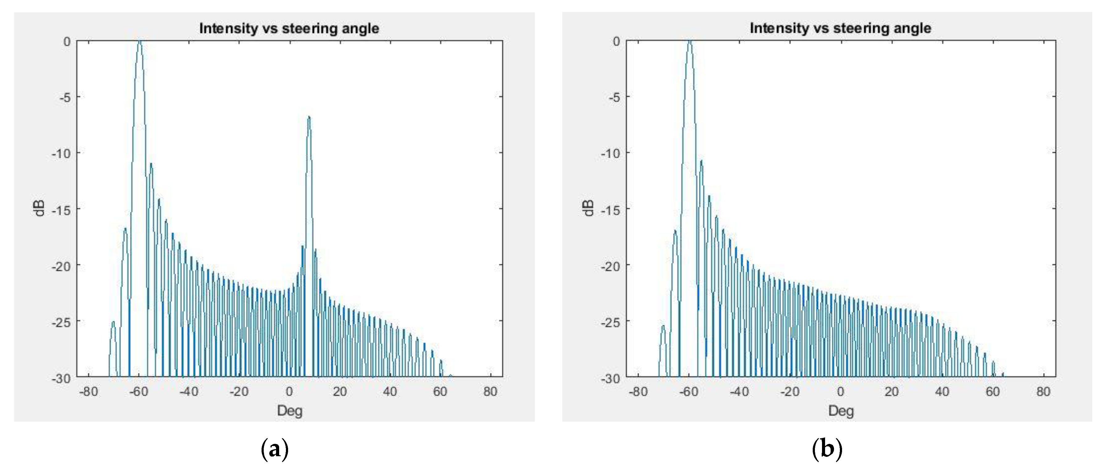
When the emitter output modes are different, the grating lobe can be observed and shown in
Figure 2a. After the additional adiabatic tapers are added as 12.4 μm and the output waveguide modes from 400- and 500-nm in width are the same, the grating lob-free can be demonstrated again as shown in
Figure 2b, and the total phase difference can be maintained as 2π.
For most LiDAR applications, a full width at half maximum (FWHM) is referred as the angular resolution, and it is the most important indicator along with side mode suppression ratio (SMSR). The optical phase array emitters are spaced much farther apart than the desired half-wavelength pitch and the performance tradeoff is between the field of view and beamforming efficiency. The sub-wavelength spacing between emitters causes strong evanescent coupling and induces the grating and side lobes. On the other hand, the large emitter pitch will generate the grating lobes to share the main beam power, significantly drop the steering efficiency, and lower the field of view.
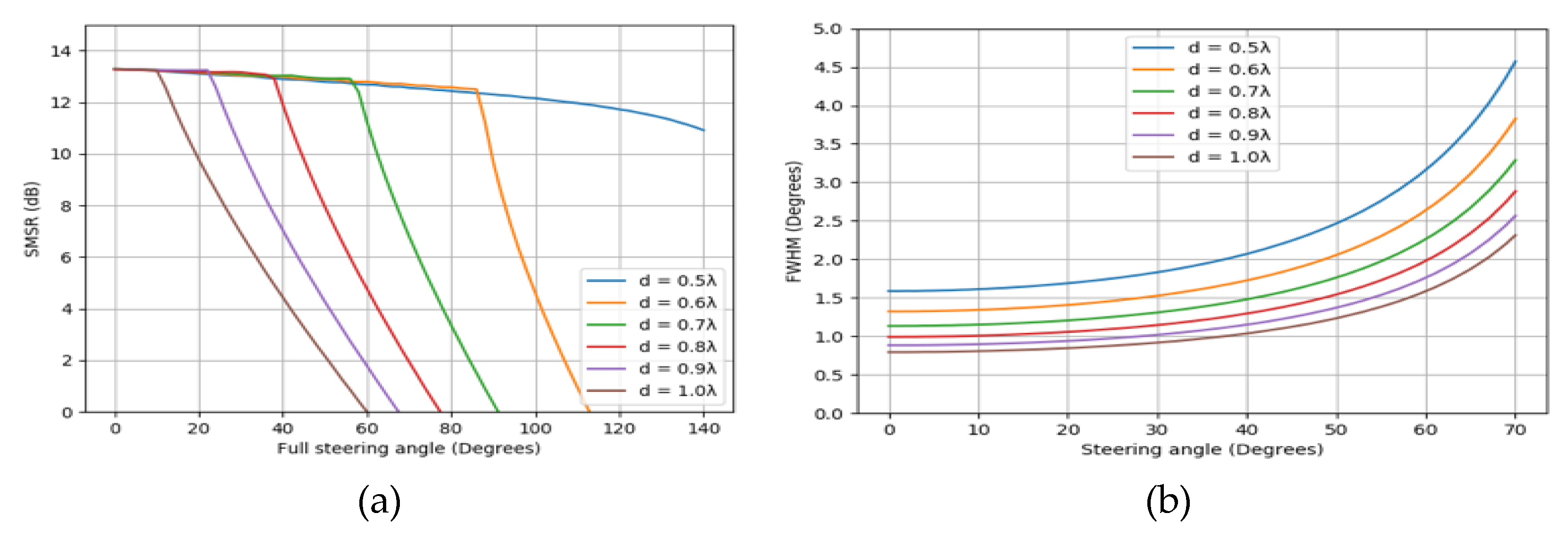
Typically, the FWHM is smaller with an increased waveguide number and higher SMSR can also be applied [
11]. When the equal spacing emitter with a 64-emitter array is considered, the RSD is taken to simulate the SMSR and FWHM versus the full steering angles at the different emitter pitch, d, as shown in
Figure 3a,b, respectively. In order to obtain a larger SMSR and better FWHM angular resolution, six different emitter pitches, 0.5-λ, 0.6-λ, 0.7-λ, 0.8-λ, 0.9-λ, and 1.0-λ, are taken for simulation. When the pitch is increased, the SMSR will get worse at fixed steering angles, but the FWHM is becoming smaller for higher angular resolution. The SMSR under the pitch of 1.0 λ drops to the minimum value at 60 degrees of the full degree angle, and will be enhanced to 13-dB when the pitch is reduced to 0.5 λ. A FWHM at 0.5 λ increases 0.5 degrees compared with 1.0 λ at 140 degrees of the full degree angle. The small pitch without the crosstalk between the emitter array is the highly demanding criterion for the beam steering. In our half wavelength spacing of 775-nm, the SMSR and FWHM can demonstrate 11 dB and 4.6 degrees, respectively, for a full steering angle of 140 degrees.
In order to get the adiabatic connection from two different pitches between the phase shifter and emitter, optical path equalization is implemented and shown in
Figure 4a. The phase compensation and mode equalization on the two index-mismatched silicon wire-based emitter array can be found in
Figure 4b and the total length of the emitter is 847.1 μm.
A schematic structure of optical phase array with 64 waveguides is demonstrated for binary splitters, phase shifter array, and emitter array. The operating wavelength is set at 1.55 µm and waveguide construction is assumed as 220-nm for height. For the half wavelength spacing, the main lobe from 64 emitters using phase-compensated two index-mismatched silicon wires-based emitters demonstrates the grating lob-free at the field of view of −25°, 0° and 25°, as shown in
Figure 5.
Since the emitters are close to each other and share the same wavelength, a test pattern for the two index-mismatched silicon wire emitters—other than using silicon wires integration—can be implemented for monitoring the phase and mode variation. Then an optical low-coherence interferometry (OLCI) including a fiber-optic Mach–Zehnder interferometer and a continuous-wave broadband source could be utilized to gauge the optical path difference [
15]. After the characterization on two emitters with 400-nm and 500-nm in width, the phase difference can be illustrated.


