Article

Color-Adjustable Devices Based on the Surface Plasmons Effect

Center of Material Science, National University of Defense Technology, Changsha 410073, China
*
Author to whom correspondence should be addressed.
Appl. Sci. 2020, 10(6), 1960; https://doi.org/10.3390/app10061960
Submission received: 25 February 2020 / Revised: 7 March 2020 / Accepted: 9 March 2020 / Published: 13 March 2020

Abstract

:
The optical response of a metamaterial can be engineered by manipulating the size, pattern, and composition of its cells. Here, we present a coloring device, which increases resolution while retaining adjustability. By adding different nanoparticles in the nanohole, the shift of the transmission peak in the visible regions is realizable and manageable, which means a series of different colors are revealed in this device. At the same time, it is also possible to fill the holes with dielectric materials of different refractive indices to achieve the purpose of color diversity. This method theoretically confirms the feasibility of designing a coloring device via surface plasmons-based metamaterial nanostructure, which holds great promise for future versatile utilization of multiple physical mechanisms to render multiple colors in a simple nanostructure.

1. Introduction

Color is a visual effect on light, produced by the eyes, brain, and our life experiences. The reflection, diffraction, scattering and absorption of light via objects provide us with extremely vivid information, especially in color. Surface plasmons (SPs), which include surface plasmon polaritons (SPPs) and localized surface plasmons (LSPs), are surface electromagnetic waves formed by the collective oscillation of free electrons in metals interacting with the incident light field [1,2,3]. It makes light in specific wavelength ranges be absorbed or radiated, and thus, a material presents different colors for human eyes. Due to the fact that the resonance frequency of a surface plasmon’s material depends largely on its structure and size, we can adjust it by changing the three-dimensional size and the pattern of the structure [4,5]. In recent years, many studies have focused on subwavelength structures of different geometries, such as the detuned square ring [6], cone holes [7], double-overlapped annular apertures [8], and hybrid structures [9]. With the development of micro-nano processing technology and characterization methods, artificially producing metal nano-microstructures to generate color has become the main method of generating structure colors in recent years [10,11]. Compared to chemical dyes, artificial microstructured materials are recyclable, easy to fabricate, and durable [12]. In addition, its local field enhancement effect can break through the diffraction limit and improve imaging resolution. These characteristics make the surface plasmon’s structure color in ultra-high resolution imaging [13,14,15], inverse design [16], CMOS digital integrated circuits [17,18,19], light emitting diodes [20], steganography [21], and many other fields in which they have major applications [22,23,24,25,26,27,28]. For example, it presents a metamaterial absorber based on vanadium-dioxide, which realizes adjustable functions in multiple and wide bands [29]; the same avatar pattern can display different color combinations by changing the angle of the polarizer [30]. In general, studies change the period and material of a micro-nano structure to adjust the position of resonance frequency so that the devices, based on the enhanced optical transmission (EOT) effect of surface plasmons, can achieve better performance. The above methods can adjust the performance of the color rendering, but it is expensive and not reusable.
In this paper, we propose an adjustable coloring device based on the surface plasmon’s structure color, which is composed of a template and metal nanoparticles. The template consists of a layer of metallic aluminum film, deposited on a quartz substrate. Then, a series of periodic circle-hole arrays are designed on the aluminum film. Adding different nanoparticles into the circle holes can cause the resonance frequency in the visible light ranges to move, thereby achieving different color displays. Moreover, we can also make the color change by filling dielectric materials with different refractive indices in the hole of the template.

2. Design and Modeling

Figure 1a is a unit cross-sectional diagram, where the gray part is SiO2 and the red part is aluminum (Al). Px and Py present the arrays periods along X and Y axes, respectively. The Al film thickness is 50 nm, which is placed on a quartz substrate with a thickness of 100 nm. The incident light incidents vertically from one side of the quartz substrate to the surface of the metallic film in the -Z direction, with the electric field in the X direction. A D65 standard light source is used as the incident light in this paper. Figure 1b is a cross-sectional diagram of periodic circle structure arrays. At the same time, it is a template in our device. By using the finite difference time domain (FDTD) method, we can simulate the propagation process of light in periodic subwavelength metallic holes. The EOT effect of the subwavelength hole arrays in the metal film can be characterized by the transmittance T as follows [31]: T = Pout(λ)/Pin(λ), where Pin is the intensity of the incident light and Pout is the light intensity detected at 100 nm from the metal surface.

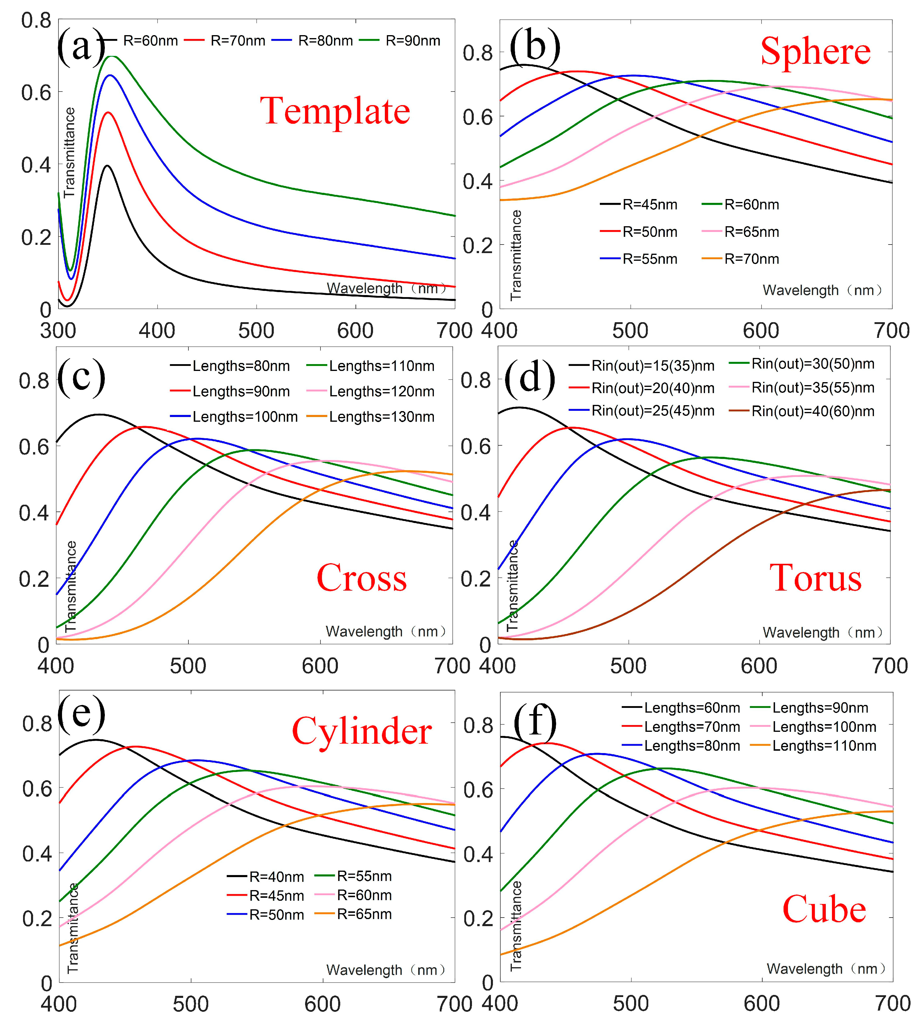
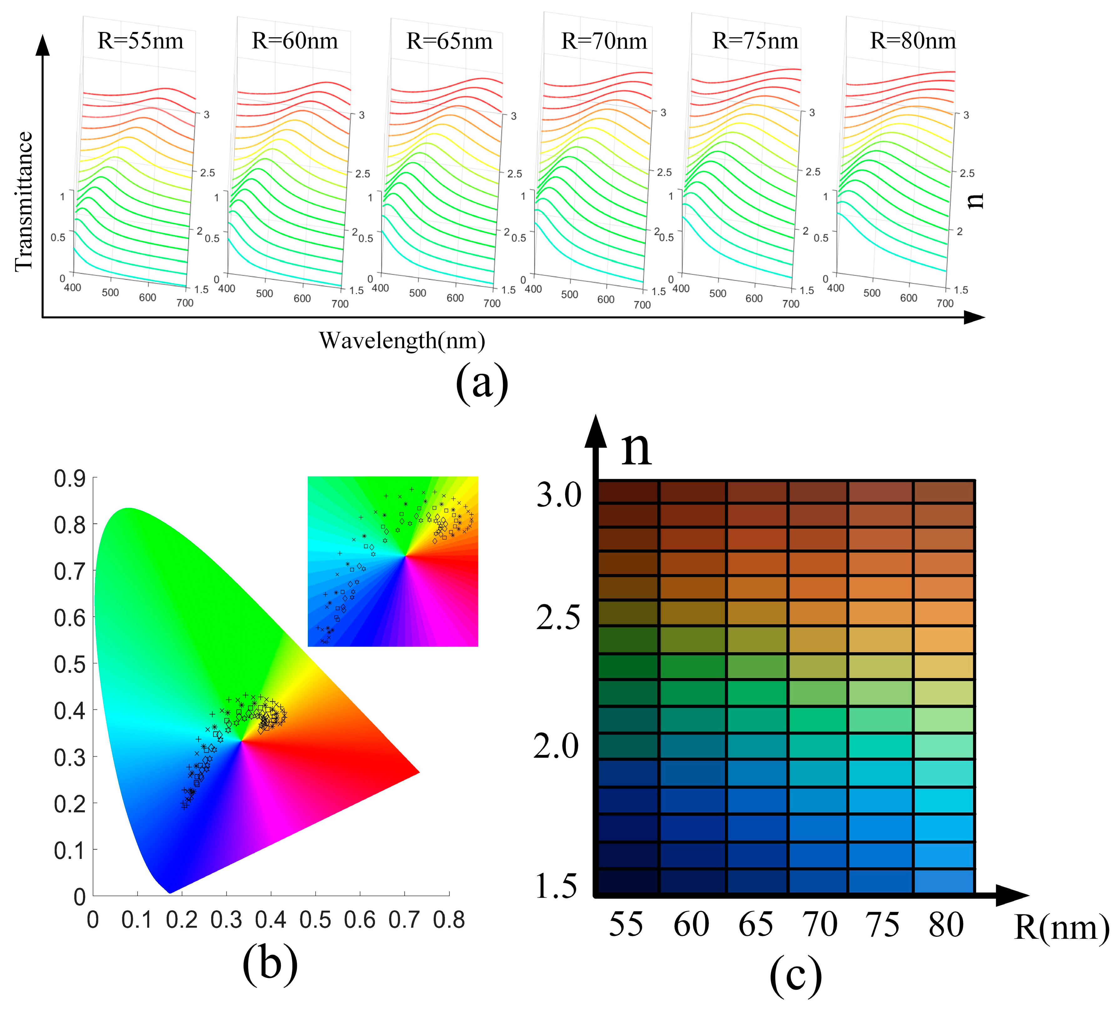
3. Results and Discussion

Considering that the template was composed of an array of circle holes, we first studied the EOT effect of the template. As shown in Figure 2a, we altered the radius of the circle hole. The parameters were set as follows: the period Px = Py = 200 nm; the thicknesses of the substrate and the metal thin film were unchanged, h1 = 50 nm and h2 = 100 nm, respectively; the radii R of the circle hole were 60 nm to 90 nm, and the step was 10 nm. It can be seen from the figure that a transmission peak is generated at 355 nm. As the radius increases, the transmission peak basically does not shift. For square hole arrays with Px = Py = P, when the light source is incident perpendicularly to the metal film, the position λmax of the EOT peak generated by the SPPs mode is mainly determined by the arrays period P [1,31]. However, the peak value increases. This is due to the increase in the hole’s space, so that more incident light can pass through. This means that there is almost no significant effect in the visible light regions for the device when the hole’s radius and structural period are constant. In order to allow the nanoparticles in the hole to have more space, we chose a radius of 90 nm for the circle hole.
As shown in Figure 1c, we designed five kinds of nanoparticles: sphere, cross, torus, cylinder, and cube. In the simulations, we gave transmission spectrums for each type of nanoparticle, which had six different geometric parameters. The geometric parameters of the five nanoparticles were set as follows: (1) Sphere: the radii R1 of the sphere were 45 nm to 70 nm and the step was 5 nm. (2) Cross: the widths W2 of the rectangle of the cross remained unchanged at 20 nm, and we only changed the lengths of the rectangle. The lengths L2 were 80 nm to 130 nm, the step was 10 nm, and the nanoparticle thickness H2 was 50 nm. (3) Torus: the radii R3-1(3-2) of the torus were 15(35) to 40(60) nm, the step was 5 nm, and the nanoparticle thickness H3 was 50 nm. (4) Cylinder: the radii R4 of the cylinder were 40 nm to 65 nm, the step was 5 nm, and the nanoparticle thickness H4 was 50 nm. (5) Cube: the side lengths L5 of the cube were 60 nm to 110 nm, the step was 10 nm, and the nanoparticle thickness H5 was 50 nm. In order to understand more clearly how nanoparticles were filled into the template, the schematic diagram of the structures of five kinds of nanoparticles filled into the template is given in Figure 1d. As shown in Figure 2b–f, as the size of the metal nanoparticles increases, red-shift happens to the transmission peaks. Apparently, the positions of the transmission peaks, which cover the entire visible light regions, have played an extremely important role in constructing a coloring device for the surface plasmon’s structure from the six sets of simulation data.
Considering the influence of isolated nanoparticles on the template, we directly placed nanoparticles on the quartz substrate to explore the effect of enhanced light transmission. The geometric parameters of nanoparticles are consistent with those of the front, and only the aluminum film is removed. Figure 3 shows the transmittance of nanoparticles with different geometry. It can be seen that with the increase in the size of nanoparticles, the transmission peak gradually red-shifts and the transmittance decreases. Generally speaking, plasmonic nanostructures with resonant excitation allow, to the extreme limit, the incident light in nanoscale space, so as to form an enhanced electromagnetic (EM) field. As we all know, the narrower the width of the slit is, the stronger the coupling of the charge densities on the two walls of the slit could be in the metallic nano-structure. The effective refractive index neff increases with decreasing the width of the nano-slits. It leads to the red-shift of the transmission peak to appear [32,33]. In our experiment, for the isolated nanoparticles, when the geometric size increases, the gap between different periods decreases, which leads to the enhancement of the resonance of the local surface plasmon resonance in the space, the increase in the effective refractive index, and the transmission peak is red-shifted. Similarly, when the size of nanoparticles in the template increases and the space in the hole decreases, the effective refractive index in the hole increases and the transmission peak red-shift occurs.
So far, for the sake of better characterizing the color performance of our coloring device, we inverted the simulation-measured transmission spectrum to the CIE1931 chromaticity coordinate chart, in order to obtain the color coordinate points. Among them, the coordinate points on each CIE1931 chromaticity space map are obtained by the simulation measured transmission spectrum banding formula [34]:
X = k λ T ( λ ) I ( λ ) x ( λ ) ,  
Y = k λ T ( λ ) I ( λ ) y ( λ ) ,  
Z = k λ T ( λ ) I ( λ ) z ( λ ) ,  
k = 100 / λ I ( λ ) z ( λ ) ,
x = X/(X + Y + Z),
y = Y/(X + Y + Z),
where T(λ) is the transmission spectrum we detected; I(λ) is the spectrum of the incident light source (D65); and x’(λ), y’(λ), and z’(λ) represent the tristimulus value. The wavelength ranges are 400 nm to 700 nm, which basically covers the visible light ranges. Additionally, (x, y), obtained from Equations (5) and (6), are the chromaticity coordinates of the transmission spectrum. As shown in Figure 4b–f, the color display of five different nanoparticles can cover the visible light regions. The specific color distribution is shown in Figure 4a.
In general, we have investigated the structure-color display via periodic subwavelength nanoparticle-hole arrays in a metal film by using FDTD software. From Figure 4d, it is apparent that when the nanoparticles choose the torus structures, the ranges of color distribution are more extensive, and the contrast between the colors presented by each parameter is also relatively clear. It is also well confirmed in the color display of Figure 4a. Therefore, in practical applications, we can adopt torus structure nanoparticles preferentially. In addition, when the sizes of nanoparticles with different structures are different, the saturation and intensity of color rendering effect are also different. Consequently, we can provide 30 different color renderings in the device we built, including different light intensity and saturation.
Considering the effect of effective refractive index changes on transmittance, we directly filled the holes with dielectric materials of different refractive indices. As shown in Figure 5a, we set the radius R of the circular hole to 55 nm–80 nm, and under each radius condition, we filled the hole with different dielectric materials with a refractive index of 1.5–3.0; the position of the transmission peak can cover the entire visible light band in the range of the refractive index 1.5–3.0. Similarly, we invert the simulation measured transmission spectrum to the CIE1931 chromaticity coordinate chart in Figure 5b in order to obtain the color coordinate points. Unlike the addition of nanoparticles, we can see from Figure 5a that the transmission peak has a smaller peak width, and the transmission peak has a larger Q value, so it has a better color contrast in the color display in the Figure 5c. In addition, the refractive index of the filled material is easier to control in practical application, so it has better realizability in the biosensor and color display. Moreover, by changing the effective refractive index of the medium to the color display, the device can be more intuitive and simple in sensing application.

4. Conclusions

In brief, we have implemented a tunable coloring device based on the surface plasmons structure color by adding different metal nanoparticles into the template. It is found that the surface plasmons distribution in the hole can be changed by adding nanoparticles with different structures on the template, so that the transmission peaks can be moved to show different colors. In addition, when filling circular holes with dielectric materials of different refractive indices, we found that the purpose of color change can also be achieved. This phenomenon can be well applied to the refractive index sensor device, and the refractive index of the environment can be represented by using different color displays. Our approach has the advantages of being nonvolatile, recyclable, inexpensive, and suitable for various environments. There are many attractive potential applications for such color rendering, including mobiles, in-window displays, the internet of things (IoT) devices, wearables, and even artificial retinas. Thus, our results could provide a new method for designing plasmonic devices and enrich the application range of metal structures in the field of optical imaging and information processing.

Author Contributions

Conceptualization, K.W. and J.Y.; Data Curation, K.W.; Methodology, K.W.; Software, K.W.; G.L.; X.J. and J.H.; Project Administration, J.Y.; Supervision, J.Y.; Writing—Original, K.W.; Writing—Review, J.Y.; Data Analysis, K.W. All authors have read and agreed to the published version of the manuscript.

Funding

This work is supported by the National Natural Science Foundation of China (60907003, 61805278), the China Postdoctoral Science Foundation (2018M633704), the Foundation of NUDT (JC13-02-13, ZK17-03-01), the Hunan Provincial Natural Science Foundation of China (13JJ3001), and the Program for New Century Excellent Talents in University (NCET-12-0142).

Conflicts of Interest

The authors declare no conflict of interest.

References

  1. Ghaemi, H.F.; Thio, T.; Grupp, D.E.; Ebbesen, T.W.; Lezec, H.J. Surface plasmons enhance optical transmission through subwavelength holes. Phys. Rev. B 1998, 58, 6779–6782. [Google Scholar] [CrossRef] [Green Version]
  2. Barnes, W.L.; Dereux, A.; Ebbesen, T.W. Surface plasmon subwavelength Optics. Nature (London) 2003, 424, 824–830. [Google Scholar] [CrossRef]
  3. Lin, L.; Roberts, A. Light transmission through nanostructured metallic films: Coupling between surface waves and localized resonances. Opt. Express 2011, 19, 2626–2633. [Google Scholar] [CrossRef] [PubMed]
  4. Hedayati, M.K.; Faupel, F.; Elbahri, M. Review of Plasmonic Nanocomposite Metamaterial Absorber. Materials 2014, 7, 1221–1248. [Google Scholar] [CrossRef] [PubMed]
  5. Murray, W.A.; Barnes, W.L. Plasmonic Materials. Adv. Mater. 2007, 19, 3771–3782. [Google Scholar] [CrossRef]
  6. Shen, X.; Wang, Y.; Chen, Q.; Wu, X. Detuned square ring resonators for multiple plasmon-induced transparencies in metal–insulator–metal waveguide. Appl. Phys. Express 2015, 8, 112201–112204. [Google Scholar] [CrossRef]
  7. Jandaghian, A.; Lotfalian, A.; Kouhkan, M.; Mohajeranl, E. Performance improvement of long-range surface plasmon structure for use in an all-optical switch. Opt. Eng. 2016, 56, 121901–121906. [Google Scholar] [CrossRef]
  8. Wang, J.; Jiang, X.X.; Xia, L.P.; Tang, L.L.; Hu, S.; Lv, J.T.; Zhao, H.Q.; Si, G.Y.; Shi, R.Y. Fabrication and optical measurement of double-overlapped annular apertures. Opt. Mater. 2016, 60, 13–16. [Google Scholar] [CrossRef]
  9. Wen, K.; Luo, X.Q.; Chen, Z.Y.; Zhu, W.H.; Guo, W.; Wang, X.L. Enhanced Optical Transmission Assisted Near-Infrared Plasmonic Optical Filter via Hybrid Subwavelength Structures. Plasmonics 2019. [Google Scholar] [CrossRef]
  10. Padovani, S.; Puzzovio, D.; Sada, C.; Mazzoldi, P.; Borgia, I.; Sgamellotti, A.; Brunetti, B.G.; Cartechini, L.; D’Acapito, F.; Maurizio, C.; et al. XAFS study of copper and silver nanoparticles in glazes of medieval middle-east lustreware (10th–13th century). Appl. Phys. A 2006, 83, 521–528. [Google Scholar] [CrossRef]
  11. Wang, G.; Chen, X.; Liu, S.; Wong, C.; Chu, S. Mechanical chameleon through dynamic real-time plasmonic tuning. ACS Nano 2016, 10, 1788–1794. [Google Scholar] [CrossRef] [PubMed] [Green Version]
  12. Al-Salem, S.M.; Lettieri, P.; Baeyens, J. Recycling and recovery routes of plastic solid waste (PSW): A review. Waste Manag. 2009, 29, 2625–2643. [Google Scholar] [CrossRef] [PubMed]
  13. Wang, J.; Fan, Q.; Zhang, S.; Zhang, Z.; Zhang, H.; Liang, Y.; Cao, X.; Xu, T. Ultra-thin plasmonic color filters incorporating free-standing resonant membrane waveguides with high transmission efficiency. Appl. Phys. Lett. 2017, 110, 031110–031113. [Google Scholar] [CrossRef]
  14. Shu, F.; Yu, F.; Peng, R.; Zhu, Y.; Xiong, B.; Fan, R.; Wang, Z.; Liu, Y.; Wang, M. Dynamic plasmonic color generation based on phase transition of vanadium dioxide. Adv. Opt. Mater. 2018, 6, 1700939. [Google Scholar] [CrossRef]
  15. Wang, B.; Dong, F.L.; Li, Q.T.; Yang, D.; Sun, C.W.; Chen, J.J.; Song, Z.W.; Xu, L.H.; Chu, W.G.; Xiao, Y.F.; et al. Visible-frequency dielectric metasurfaces for multiwavelength achromatic and highly dispersive holograms. Nano Lett. 2016, 16, 5235–5240. [Google Scholar] [CrossRef] [PubMed]
  16. Huang, Z.; Liu, X.; Zang, J.F. The inverse design of structural color using machine learning. Nanoscale 2019, 11, 21748–21758. [Google Scholar] [CrossRef]
  17. Guo, T.B.; Evans, J.; Wang, N.; He, S.L. Monolithic chip-scale structural color filters fabricated with simple UV lithography. Opt. Express 2019, 27, 21646–21651. [Google Scholar] [CrossRef]
  18. Yokogawa, S.; Burgos, S.P.; Atwater, H.A. Plasmonic color filters for CMOS image sensor applications. Nano Lett. 2012, 12, 4349–4354. [Google Scholar] [CrossRef]
  19. Yu, Y.; Chen, Q.; Wen, L.; Hu, X.; Zhang, H. Spatial optical crosstalk in CMOS image sensors integrated with plasmonic color filters. Opt. Express 2015, 23, 21994–22003. [Google Scholar] [CrossRef]
  20. Xin, J.Z.; Hui, K.C.; Wang, K.; Chen, H.L.W.; Ong, D.H.C.; Leung, C.W. Thermal tuning of surface plasmon resonance: Ag gratings on barium strontium titanate thin films. Appl. Phys. A 2012, 107, 101–107. [Google Scholar] [CrossRef]
  21. Zhao, R.; Sain, B.; Wei, Q.; Tang, C.; Li, X.; Weiss, T.; Huang, L.; Wang, Y.; Zentgraf, T. Multichannel vectorial holographic display and encryption. Light. Sci. Appl. 2018, 7, 95–104. [Google Scholar] [CrossRef] [PubMed] [Green Version]
  22. Kuznetsov, A.I.; Miroshnichenko, A.E.; Brongersma, M.L.; Kivshar, Y.S.; Luk’yanchuk, B. Optically resonant dielectric nanostructures. Science 2016, 354, 2472–2479. [Google Scholar] [CrossRef] [PubMed] [Green Version]
  23. Chen, B.H.; Wu, P.C.; Su, V.C.; Lai, Y.C.; Chu, C.H.; Lee, I.C.; Chen, J.W.; Chen, Y.H.; Lan, Y.C.; Kuan, C.H.; et al. GaN metalens for pixel-level full-color routing at visible light. Nano Lett. 2017, 17, 6345–6352. [Google Scholar] [CrossRef] [PubMed]
  24. Zhou, H.; Zhen, B.; Hsu, C.W.; Miller, O.D.; Johnson, S.G.; Joannopoulos, J.D.; Soljacic, M. Perfect single-sided radiation and absorption without mirrors. Optica 2016, 3, 1079–1086. [Google Scholar] [CrossRef]
  25. Lee, T.; Jang, J.; Jeong, H.; Rho, J. Plasmonic- and dielectric- based structural coloring from fundamentals to practical applications. Nano Converg. 2018, 5, 1–21. [Google Scholar] [CrossRef] [Green Version]
  26. Zhang, C.; Wu, K.; Ling, B.; Li, X. Conformal TCO-semiconductor-metal nanowire array for narrowband and polarization-insensitive hot-electron photodetection application. J. Photon. Energy 2016, 6, 042502–042511. [Google Scholar] [CrossRef]
  27. Tcherniak, A.; Ha, J.W.; Dominguez-Medina, S.; Slaughter, L.S.; Link, S. Probing a century old prediction one plasmonic particle at a time. Nano Lett. 2010, 10, 1398–1404. [Google Scholar] [CrossRef]
  28. Tamitake, I.; Yamamoto, Y.; Takayuki, O. Absorption cross-section spectroscopy of a single strong-coupling system between plasmon and molecular exciton resonance using a single silver nanoparticle dimer generating surface-enhanced resonant raman scattering. Phys. Rev. B 2019, 99, 235409–235420. [Google Scholar]
  29. Song, S.C.; Ma, X.L.; Pu, M.B.; Li, X.; Guo, Y.H.; Gao, P.; Luo, X.G. Tailoring active color rendering and multiband photodetection in a vanadium-dioxide-based metamaterial absorber. Photonics Res. 2018, 6, 492–497. [Google Scholar] [CrossRef] [Green Version]
  30. Luc, D.; Angélique, L.; Benjamin, G.; Lukas, N. Plasmonic films can easily be better: Rules and recipes. ACS Photonics 2016, 3, 190–196. [Google Scholar]
  31. Ruan, Z.C.; Qiu, M. Enhanced transmission through periodic arrays of subwavelength holes: The role of localized waveguide resonances. Phys. Rev. Lett. 2006, 96, 233901–233904. [Google Scholar] [CrossRef] [PubMed]
  32. Shi, H.F.; Wang, C.T.; Du, C.L.; Luo, X.G.; Dong, X.C.; Gao, H.T. Beam manipulating by metallic nano-slits with variant widths. Opt. Express 2005, 13, 6815–6820. [Google Scholar] [CrossRef] [PubMed]
  33. Bliokh, K.Y.; Bliokh, Y.P.; Freilikher, V.; Savel’ev, S.; Nori, F. Colloquium: Unusual resonators: Plasmonics, metamaterials, and random media. Rev. Mod. Phys. 2008, 80, 1201–1213. [Google Scholar] [CrossRef] [Green Version]
  34. Ameri, T.; Dennler, G.; Waldauf, C.; Azimi, H.; Seemann, A.; Forberich, K.; Hauch, J.; Scharber, M.; Hinger, K.; Brabec, C.J. Fully solution-processing route toward highly transparent polymer solar cells. Adv. Funct. Mater. 2010, 20, 1592–1598. [Google Scholar] [CrossRef]
Figure 1. (a) Structural cross-sectional diagram of the unit structure in the X–Y plane. R represents the circle structure radius; h1 and h2 are the thickness of the Al and SiO2; Px and Py are the periods; as follows: R = 90 nm; h1 = 50 nm; h2 = 100 nm; Px = Py = 200 nm. (b) Cross-sectional diagrams of the periodic circle structure arrays. (c) Different nanoparticles: Sphere, Cross, Torus, Cylinder and Cube—they are all made of aluminum. (d) Schematic of the template structure filled with different nanoparticles.
Applsci 10 01960 g001
Figure 2. Transmittances of the template and different nanoparticles. (a) Template; (b) Sphere; (c) Cross; (d) Torus; (e) Cylinder; (f) Cube.
Applsci 10 01960 g002
Figure 3. Transmittances of the isolated nanoparticles. (a) Sphere; (b) Cross; (c) Torus; (d) Cylinder; (e) Cube. In these cases, we only removed the aluminum film and kept the other parameters unchanged.
Applsci 10 01960 g003
Figure 4. (a) Color display of the different nanoparticles at different geometric parameters. (bf) CIE1931 color space inversion map distribution under different conditions.
Applsci 10 01960 g004
Figure 5. (a) Transmittances under the different refractive indices 1.5–3.0 and the hole radius 55 nm–80 nm. (b) CIE1931 color space inversion map distribution under different conditions. Among them, the illustration is a partially enlarged drawing. (c) Color display under the different refractive indices and hole radius.
Applsci 10 01960 g005

