Article

Simultaneous Nano-Texturing onto a CVD-Diamond Coated Piercing Punch with Femtosecond Laser Trimming

1
Surface Engineering Design Laboratory, SIT, Tokyo 144-0045, Japan
2
Faculty of Engineering, University of Toyama, Toyama 930-8555, Japan
3
LPS-Works, Co., Ltd., Tokyo 144-0033, Japan
*
Author to whom correspondence should be addressed.
Appl. Sci. 2020, 10(8), 2674; https://doi.org/10.3390/app10082674
Submission received: 26 February 2020 / Revised: 5 April 2020 / Accepted: 7 April 2020 / Published: 13 April 2020
(This article belongs to the Special Issue Micro/Nano Manufacturing II)

Abstract

:

Featured Application

Precise metal forming of electrical steel and magnetic amorphous sheets, Precise piercing of metallic sheets into fine connectors, transducers and lead-flames.

Abstract

In this study, a CVD (Chemical Vapor Deposition)-diamond coated tungsten carbide cobalt (WC (Co)) punch was trimmed to adjust its surface roughness and to significantly reduce its edge curvature for fine piercing by femtosecond laser processing. Through this laser trimming, the surface quality of the diamond coating and the punch edge profile were improved to less than 0.5 μm at the maximum roughness and 2 μm in the edge width, respectively. In parallel with this improvement of surface quality, the side surface of the diamond coating was modified to include nano-textures via the LIPSS (Laser Induced Periodic Surface Structuring) process. Through the fine piercing process, this nanotexture was transcribed onto the pierced hole surface together with fine shearing of the hole by piercing. WLI (White-Light Interferometry) and SEM (Scanning Electron Microscopy) were utilized to describe this transcription of nanotextures during the piercing process. These semiregular nanotextures with an LIPSS period of 300 nm on the pierced hole surface induced a blue colored surface plasmon.

1. Introduction

Motor cores have grown to become one of the most essential parts of electric vehicles and passenger cars. Since pierced electrical steel sheets and magnetic amorphous films are stacked in the motor core, each constituent sheet and film must be precisely punched out to minimize geometric irregularities, such as burrs and fractured surfaces, as well as the affected zones in these work materials to achieve a significant reduction of iron loss [1]. Tungsten carbide cobalt (WC (Co)) punches and dies with a normal WC-grain size are selected as a standard punch and core die during die-manufacturing and stamping of the iron core because of their greater hardness than tool steel [2]. They often suffer from severe chipping and failure even in the early stages of the piercing process, as stated in [3]. Since normal WC-grains can easily drop from the punch edge during piercing, the punch edge curvature is always designed to be more than 10 μm, which is enough to be free from chipping. Hence, the burr height and the affected zones increase inevitably by increasing the number of shots in piercing, as noted in [4,5]. Three methods were developed to accomplish fine piercing without failure [5].
Refinement of WC-grains was the first approach used to promote edge strength in piercing. As proposed in [6], ion milling is available to sharpen the punch edge down to 1 to 2 μm and to remove the mechanically affected layers by grinding and polishing. The second method involves using low temperature plasma nitriding to harden and control the microstructure of SKD11/AISI316 punches and dies to significantly improve dry piercing performance [7,8]. Due to their higher hardness than 1400 HV, as well as their finer grain size than 0.1 μm, no chipping and failure occur at the punch edge, even after continuous dry piercing over 1000 repetitions. In addition, the nearly-zero clearance between the punch and core-die increases the burnished area ratio by up to 85% and reduces the burr height down to 10% of the work sheet thickness. A diamond protective coating of the normally grained WC (Co) punch is the third method used to avoid chipping, even after long-term usage [9]. Due to the dull edge and rough punch surfaces of this diamond-coated WC (Co) punch, the fractured surface is left in part in the pierced hole of the stainless steel workpiece. This third method requires some surface treatments to shape the diamond coating.
Among these treatments, the laser trimming process is effective not only to reduce surface roughness but also to adjust the punch surface configuration. The excimer laser treatment was first utilized for the trimming of a diamond-coated WC (Co) punch [9]. The diamond-coated punch head geometry was adjusted accurately within tolerance ranges from +0.1 to +0.6 μm without a significant change in the Raman spectrum of diamond coating by trimming. The femtosecond laser trimming method also improved the dimensional accuracy of the fine piercing punches [10,11]. The edge curvature radius of the diamond coated WC (Co) punch was reduced from 12.5 μm down to 2.5 μm. AISI316L stainless steel sheets were successfully pierced by this trimmed punch to narrow the affected zone in the cross-section of the pierced sheets.
When using this femtosecond laser irradiation, a nanotexture was formed on the irradiated surface by LIPSS (Laser Induced Periodic Surface Structuring) [12]. Since this first discovery on LIPSS, many studies have reported its theoretical and experimental factors, as well as its application to the modification of surfaces and optical properties and its tribological performance [13]. This nanotexturing has the possibility to work simultaneously with the laser trimming of diamond-coated punches. As illustrated in Figure 1a, directionally nanotextured ripples are superposed on the trimmed diamond coatings by the simultaneous optical interference between the incident light and the scattered beams due to the trimmed surface roughness. As illustrated in Figure 1b, when using this laser-trimmed punch with its nanotextured side surface for the piercing process, these nanotextures are possibly transcribed onto the pierced hole surface of the metallic sheet concurrently with the piercing process. This concurrent transcription of nanotextures on the pierced hole is a result without any precedent in the literature.
In the present study, this femtosecond laser trimming of the diamond coated WC (Co) punch by CVD (Chemical Vapor Deposition) was first employed to achieve the above possibility of simultaneous nano-texturing with laser trimming. SEM (Scanning Electron Microscopy; Ricoh, Co., Ltd., Tokyo, Japan), LM (Laser Microscopy; Keyence, Co., Ltd., Tokyo, Japan), and WLI (White-Light Interferometry; Opt-Scope, Tokyo Seimitsu, Co., Ltd., Tokyo, Japan) were utilized to characterize these simultaneously induced nanotextures on the trimmed diamond surface. An interferometry analysis was made via the algorithm for DEAP (Detection of Envelope and Absolute Phase). Secondly, this trimmed punch was inserted into a cassette die set for a fine piercing experiment with the use of a CNC (Computer Numerical Control) stamper. An AISI316L stainless steel sheet with a thickness of 0.1 mm was employed as a work material for piercing to investigate whether these nanotextures on the punch surface are transcribed concurrently by piercing a hole into the steel sheet. SEM and WLI were also used to describe this transcription process together with piercing behavior.

2. Experimental Procedure

Diamond coated WC (Co) punches (Fijidice, Co., Ltd., Tokyo, Japan) were prepared for the femtosecond laser trimming via a two-step procedure. A CNC-stamping system was also employed to pierce a AISI316L sheet with a thickness of 0.1 mm.

2.1. Femtosecond Laser Trimming System

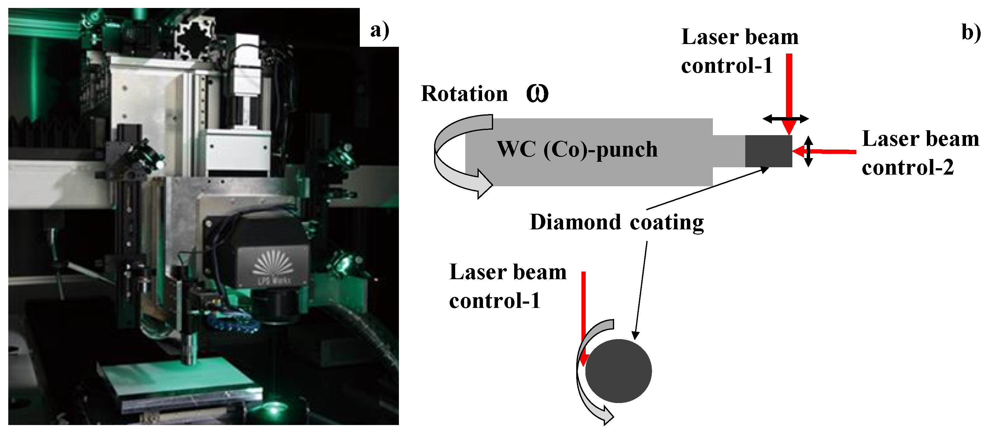
Femtosecond or sub-picosecond lasers were developed for innovative research and development; most industrial applications rely on laser machinery in the order of 100 femtoseconds. Since the focus areas of work materials are subjected to ultra-high power irradiation, finding a way to scan the beam spot has become increasingly important when using this laser machining system. The higher repetition rate of laser beams, as well as their higher scanning speeds, results in fast-rate, dimensionally accurate machining. Our developed system and its configuration are shown in Figure 2a. The wavelength of the femtosecond laser was 515 nm, the pulse width was 200 fs, and the pulse repetition rate was 400 kHz. The maximum average power was 40 W, and the maximum pulse energy was 50 μJ. The working stage was 300 mm × 300 mm. A work material with sized 280 × 150 mm was placed on the X- and Y-axes controlled stage in Figure 2a. The single-shot power was estimated to be 0.25 GW. High-powered irradiation of 200 fs was used to drive the well-defined ablation into the targeted materials [13].

2.2. Laser Trimming Procedure

The laser-trimming and polishing process was instrumented into an experimental setup with notes on the uniform machining and laser beam path control. Figure 2b illustrates the standard setup for the present trimming experiments. The side surface of the diamond coating was first trimmed using the laser beam control-1, where the laser is scanned along the central axis of the WC (Co)-punch until the total reduction in thickness reaches the specified depth. As experimentally demonstrated in the following section, the directional nanotexture was formed in situ during this laser machining process with a skew angle against the beam scanning direction. The fluence was constant with 0.6 J/cm2. The laser machining track overlapped the working range 20 times by rotating the work. As pointed out in [13,14,15], the LIPSS-ripple period is controllable by the laser fluence, pulse width, and so forth for femtosecond laser nanotexturing. In fact, LIPSS using high and low spatial frequencies with very different periods can be produced via the same laser setup depending on the process conditions. In the following, this LIPSS-ripple period is estimated to be 250 nm from the above trimming conditions.
The top surface is secondly processed by using the laser beam control-2. The laser beam was moved from the center to the end of the punch head. The fluence was also held constant at 0.265 J/cm2. During this two-step procedure in the experiment, the end of the punch was held in a jig to be rotated with a constant velocity by ω = 7.2 degrees/s. The galvanometer was utilized to distribute the laser beam as tailored by CAM (Computer Aided Machining) data for the trimming operation.

2.3. Fine Stamping System

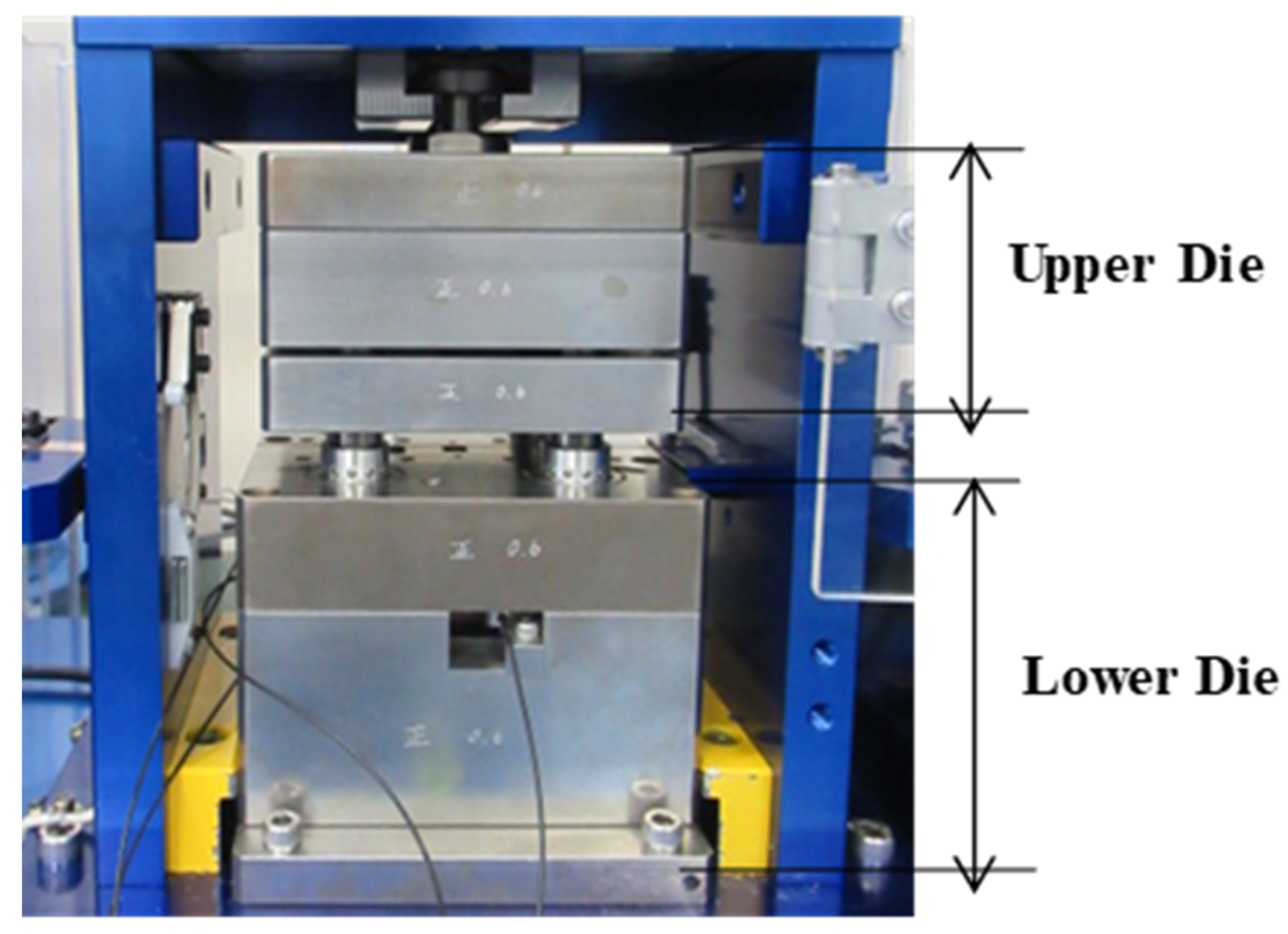
Figure 3 depicts a piercing experimental set up where the stroke is controllable every 1 μm with in situ measurements of the piercing load and the punch stroke. The laser trimmed diamond-coated WC (Co) punch with a diameter of 2.000 mm was fixed into an upper die in the cassette die-set for the piercing experiment. The WC (Co) core die with an inner diameter of 2.008 mm was also placed into the lower die. The load cell was embedded into the lower die set to monitor the applied load in every stoke.

3. Experimental Results

Three diamond coated WC (Co) punches were employed to experimentally describe the simultaneous formation of unidirectional nanotextures onto the diamond coatings with the laser trimming process, as well as the concurrent coining of the nanotextures onto the burnished hole surfaces with the piercing process.

3.1. Simultaneous Nanotexturing with Femtosecond Laser Trimming

Figure 4 compares the geometry of the CVD-diamond coated WC (Co) punches before and after femtosecond laser trimming. The side surface of the diamond coating in the vicinity of the punch edge was trimmed down to 150 μm from the punch head in the axial direction of the punch with a depth of 3.5 μm. The diamond coating on the punch head was also trimmed to reduce the maximum toughness below 0.5 μm.
Figure 5 shows SEM and LM images of the diamond coated WC (Co) punch after trimming. As depicted in Figure 5a, the laser-machined traces are seen in the circumferential direction. The incident laser has the possibility to engage in optical interactions with the scattered beam via the rough diamond coating surfaces and to form nanostructured ripples through this interaction. Figure 5b proves that the original rough edge with a radius of curvature of 12.5 μm was reduced down to an edge width less than 2 μm via this laser trimming. Figure 5c also demonstrates that nanotextures with an LIPSS-period of 300 nm were formed in the axial direction from the vicinity of the punch edge in this laser trimming process by using second harmonics with a fluence of 0.6 J/cm2. The agreement between this measured nanotexture width of 300 nm and the theoretical estimate of 250 nm assures that the measured nanotextures in Figure 5c are simultaneously induced by the present femtosecond laser trimming process.
Let us consider the directivity of the unidirectional nanotextures in Figure 5c. As discussed in [13,16,17], the nanotextured ripples in the lateral direction are induced by femtosecond laser scanning in the longitudinal direction on a relatively smooth surface with a low roughness. In the present trimming process of the diamond coating on the cylindrical punch, the scattering laser was skewed by the local curvature on the trimmed diamond surface so that every nanotextured ripple was formed in the axial direction with a skewed angle. This nanotexturing process involving trimming the cylindrical diamond coating was mainly governed by the local curvature of the cylindrical punch, as well as the original roughness of the diamond coating. On the other hand, the laser trimming conditions, such as the trimmed depth of the cut (d), have less of an influence on this nanotexturing. In order to demonstrate the insensitivity of the trimmed depth to the induced nanotexturing process, three diamond punches were prepared and trimmed by d = 1.8, 2.4, and 3.6 μm.
Figure 6 compares the SEM images of the nanotextures on each trimmed surface using the three punches. Although the peak-to-valley ratio of the nanotextures increases with d, the unidirectional formation of the nanotextures with a skewed angle is common among the three punches. Similar nanotextures are simultaneously machined onto the diamond coating with trimming once the local curvature and roughness of the original diamond coating are predetermined as a tool geometry in addition to the femtosecond laser capacity.
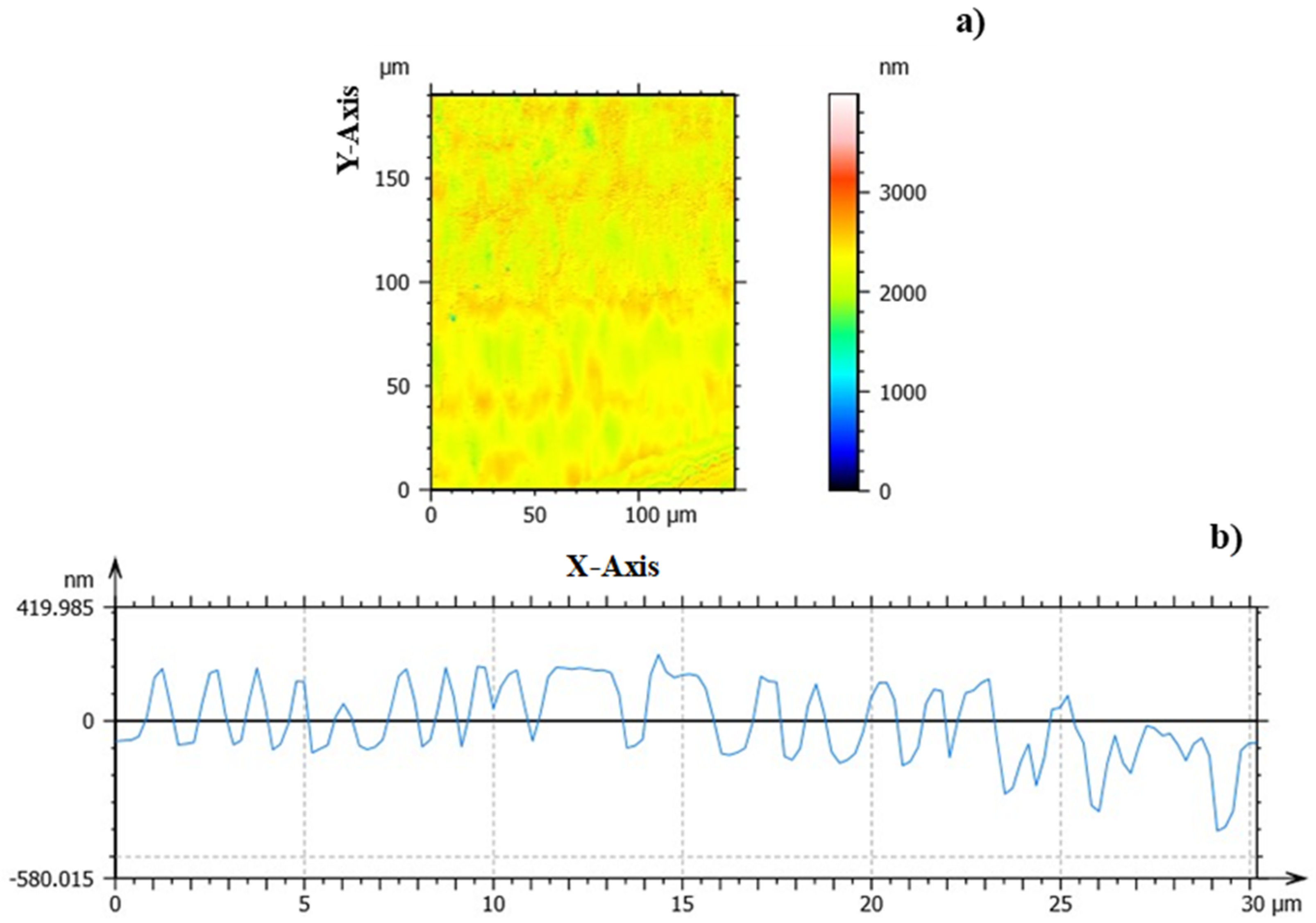
WLI is utilized as a nondestructive evaluation method for the diagnosis of nanotextures on the profiles of trimmed punch surfaces. This WLI is usually used to measure the geometric angulation of polished and buffed die surfaces with relatively small curvature radii; e.g., the local imperfections on the die surface profile are detected as a Moire pattern, from which the local surface condition is shown to involve geometric angulation with spatial frequencies [18]. The trimmed diamond-coated punch in Figure 5 was employed as a specimen for WLI to measure the spatial period of nanotextured ripples on the trimmed surface. Figure 7a depicts the two-dimensional surface angulation on the trimmed diamond coating. If the trimmed surface were flat like a laser-polished surface, no Moire patterns or no two-dimensional angulations could be seen. If the trimmed diamond coating had randomly distributed roughness, the two-dimensional profile analyzed by WLI would have an irregular convex–concave pattern. The measured two-dimensional profile in Figure 7a has a regular distribution with the spatial period. In particular, regularly modulated nanotextures in the X-axis are aligned in the Y-axis. Figure 7b shows this local surface profile in the X-axis or in the lateral direction of the punch surface, which was analyzed by the DEAP algorithm. Although this profile gradually deviates from the center line, the nanotextures are formed on the trimmed punch surface with a skewed angle in the axial direction. The measured spatial period of the nanotextures (Λpunch) is 900 nm, and their average height reaches 300 nm.

3.2. Concurrent Transcription of the Nanotextures onto the Hole Surfaces with Piercing

The trimmed diamond-coated punch and the core die were fixed into the cassette die for the piercing experiment. In the present experiment, clearance was controlled to be 4%, which is similar to fine blanking process used for automotive parts. Misalignment of the punch to the core die was avoided by the movable x–y stages of the stamper, making the eccentricity negligible. The pierced holes were observed by optical microscopy and SEM under different magnifications. As depicted in Figure 8a, the entire hole surface was metallic and shiny, without any traces of fractured areas. In fact, the burnished surface area ratio was measured to be 100%, as shown in Figure 8b. An SEM analysis with higher magnification revealed that nanotextures were formed on this burnished surface, as depicted in Figure 8c. Nanotextures with a spatial period of 0.3 μm were superposed on the fine burnished surface profile. That is, hole surface pierced by the present trimmed punch was characterized by its multi-dimensionally modified profile. It was fully burnished similar to the fine-blanked surfaces under narrowed clearance [19]. In addition, this surface burnished by the trimmed punch features a regular nanotextured microscopic profile dissimilar to the fine-blanked surface profile, with significant roughness in the order of 3 to 5 μm at maximum.
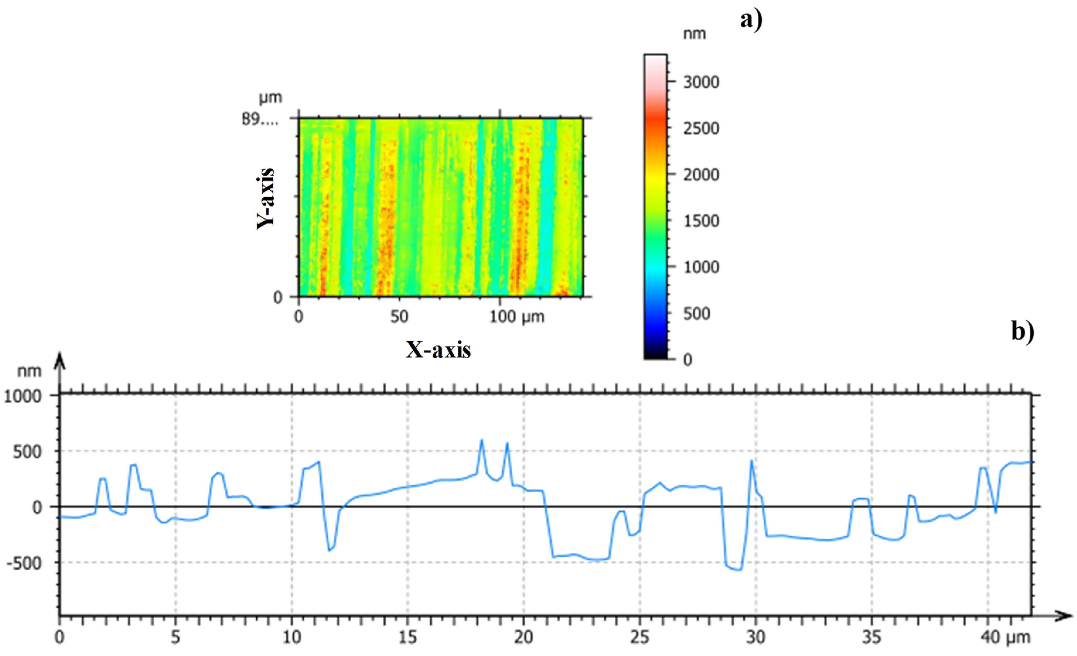
WLI was also utilized to engage in a nondestructive analysis of the transcribed nanotextures, as shown in Figure 8c. The two-dimensional surface angulation is depicted in Figure 9a. Linear nanotextures were formed along the Y-axis or in the direction of the hole thickness. These textures were periodically formed in the X-axis or in the circumferential direction of the pierced hole. Figure 9b depicts the microscopic profile of nanotextured surface. Although the average height drifted due to the noises in interferometry, the nanotextures were detected to have the same spatial period (Λ) of 900 nm, as seen in Figure 7; i.e., Λpunch = Λhole = 900 nm by WLI. Figure 8c and Figure 9a,b prove that the nanotextures on the punch side surface were transcribed onto the pierced hole surface in a semi-regular nanopattern. In the algorithm of DEAP, the effects of large punch curvatures and pierced hole surfaces on interferometric measurements are difficult to avoid when analyzing nanotextured periods. The nanotextures on the punch and hole surfaces with a period of 300 nm were expanded by this curvature effect in the WLI and DEAP analysis to estimate larger periods.
We will next describe the differences in hole surface quality for fine piercing under the same clearance when using two different punches; i.e., the bare WC (Co) punch with the normal WC-grain size and the laser-trimmed diamond-coated WC (Co) punch. As depicted in Figure 10a, a normal hole pierced by the bare WC (Co) punch has a dull, fully burnished surface with metallic scratches on the punch side surface from dry shearing without lubrication. The maximum roughness on this burnished surface reaches 3 μm. In addition, the debris particles and fragments adhered to the bare WC (Co) punch head and side surfaces. This adhesion triggered chipping at the punch edge and shortened the punch life in practice.
On the other hand, the hole pierced by the trimmed punch has a metallic, shiny surface without any scratches. In addition, blue-colored luster is also detected by optical microscopy as a surface plasmon in the nanotextures of the hole surface. This reveals that fine burnished and mirror-polished surfaces are produced by using the trimmed punch concurrent with nanotexturing. This high surface quality of the products pierced and fine-blanked using the trimmed punch is ensured by the surface-plasmonic brilliance in practical operation. In addition, these nanotextures could have a role in prolonging the punch life.
The fine and clean hole surface of the pierced AISI316L sheets was preserved even after continuously piercing it 100 times. This suggests that the debris particles generated during piercing under narrow clearance could be ejected through the nanotextures on the side surface of the punch. Figure 11 depicts an SEM image of the nanotextured side surface of the punch from its edge along its length after piercing a hundred holes into the AISI316L sheets. The white debris particles are trapped in the nanotextures and pushed up along the length of the punch.

4. Discussion

In the fine blanking of metallic sheets under narrow clearance, the work material is sheared with nearly a full burnished surface area ratio due to hydrostatic pressure [20]. This suggests that the work material under shearing is compressed to the punch side surface during the piercing process under narrow clearance. Since the clearance is 4% of the sheet’s thickness under the present piercing conditions, the nanotextures on the punch side surface are coined onto the burnished surface by this hydrostatic pressure. Macroscopically, the pierced hole surface is smooth, metallic, and shiny since the fine surface profile of the laser-trimmed punch was transferred onto the hole surface. Together with this transcription, the nanotextures on the punch side surface were also coined microscopically. This simultaneous transcription of the punch surface structure through the piercing process forms a multi-dimensional hole surface profile. This finishing process is useful in the production of automotive parts. A macroscopically smooth hole surface is essential to function as an orifice for fuel injection [21]. Microscopic textures are expected to offer new functionality to the orifice hole surface to control the flow pattern of liquid fuel before fogging it into fine droplets.
One of the most effective features for nanotextures lies in the enhancement of the optical responses of the nanotextured surfaces. Many studies on the enhancement of optical properties by surface nanotexturing revealed that the geometric regularity of nanotextures significantly reflects this nanotexturing effect [22,23]. Optical reflectivity is greatly reduced even by irregular nanotextures on the surface [22]. The regular alignment of nano-dots and nano-grooves is necessary to induce a surface plasmon effect onto the nanotextured surface [23]. As shown in Figure 7 and Figure 9, semi-regular nano-grooves are densely coined onto the hole surface by fine piercing with a laser trimmed punch. The surface plasmon in a blue color is locally seen on the nanotextured area with regular alignment on the hole surface. This surface plasmonic state is greatly improved by narrowing the clearance between the piercing punch and the core-die so that more regularly aligned nanotextures can be coined onto the hole surface.
In standard metal forming, the geometry and dimensions are transcribed onto the metallic members by fine stamping with mechanically finished dies and punches. In standard piercing, the clearance between the die and punch is optimized to increase the burnished surface area ratio and to prolong tool life. As shown in Figure 10a, the maximum roughness on the hole surface reaches 3 μm due to the scratched trances using a normal punch. By using the laser trimming process, the diamond-coated punch has a smooth head and side surfaces with a lower maximum roughness than 0.5 μm, as well as nanotextures on the trimmed side surface. This suggests that the diamond coated punch has geometric functionality, as well as a fine surface profile. Through the fine piercing process, the low roughness surface of the punch is transcribed onto the metallic-shining hole surface; e.g., the maximum roughness on the pierced hole surface in Figure 10b is less than 0.1 μm. Concurrent with this piercing, the semi-regular nanotexture alignment on the punch is coined onto this smooth hole surface. This proves that multi-dimensional, geometric features are formed on a product surface by micro-manufacturing with the use of laser-decorated tools.
Parallel with the above coining of nanotextures, the debris particles of the AISI316 sheet generated by piercing were ejected through these nanotextures on the punch from its edge along its length, as shown in Figure 11. This reveals that the nanotextures on the trimmed punch surface work as a nano-channel to eject fine debris particles of the work material from the shearing interface. This automatic ejection mechanism for dry debris is a key technology in the miniaturization or down-sizing of metallic products to prevent their surfaces from being contaminated by tiny debris particles. The friction and wear on the tool-work contact interface could be reduced to lower the maximum load and improve the surface quality of the formed products.

5. Conclusions

Fine nanotextures were successfully formed on the side surface of a diamond-coated cylindrical WC (Co) punch simultaneously with the laser trimming process. This nanotexturing process was mainly controlled by the local curvature of the cylindrical punch, as well as the roughness of the diamond coating, which had less sensitivity to the trimming conditions. Under optimized trimming conditions, the nanotextures were formed through the nano-channels up to the punch head with sufficient depth. These channels eject the debris particles of work materials from the piecing process not only when using dry but also when using wet types of lubrication [13]. As demonstrated in [24], where the adhesion of debris fragments onto the cutting surfaces was significantly ameliorated by the presence of microtextures, the piercing punch life was greatly prolonged by this emission of debris fragments from the work materials.
The nanotextures induced by laser trimming are transcribed onto the hole surface concurrently with the piercing process. Under the narrowed clearance between the trimmed punch and the core die, these nanotextures superimpose onto the fine burnished surface during piercing. This multi-dimensional formation of the product surfaces proves that smooth geometry is produced on the product together with plasmonic surface decoration.
Under normal manufacturing, the tool surface had difficulty finishing its profile with microtexturing. In addition, the product geometry also had difficulty being shaped with microtexturing. In the presently-applied femtosecond laser trimming, the piercing punch was trimmed to control the surface roughness simultaneously with the formation of nanotextures onto the trimmed tool surface. These nanotextures were transcribed onto the metallic–shining burnished surface concurrently with the shaping of the product geometry. This nanotexturing onto the tool and product surfaces together with tooling and metal forming provides a new way to decorate tool surfaces using lasers and to build up the multi-dimensional surfaces on a product.

Author Contributions

Conceptualization of the short-pulse laser trimming was done by T.A.; methodology of the laser trimming and nanotexturing, T.A., T.S., and T.I.; investigation, T.A., T.S., and Y.K., writing—original draft preparation, T.A.; writing—review and editing, T.A. and T.S. All authors have read and agreed to the published version of the manuscript.

Funding

This study was financially supported in part by METI (Ministry of Economy, Trades and Industries, Japan Government)-program on the Supporting Industries in 2019.

Acknowledgments

The authors would like to express their gratitude to H. Okabe (LPS-Works, Co., Ltd., Tokyo, Japan), T. Fukuda (Tokai Engineering Service, Co., Ltd., Tokyo, Japan), and Y. Suzuki (Komatsu-Seiki Kosakusho, Co., Ltd., Suwa, Japan) for their help in the experiments.

Conflicts of Interest

The authors declare no conflict of interest.

References

  1. Huynh, T.A.; Hsieh, M.-F. Performance evaluation of thin electrical steels applied to interior permanent magnet motor. In Proceedings of the 2016 19th International Conference on Electrical Machines and Systems (ICEMS), Chiba, Japan, 13–16 November 2016; pp. 1–6. [Google Scholar]
  2. Precise Production of Electrical Steel Motor Cores. Available online: https://www.kuroda-precision.co.jp/products/lp/ (accessed on 24 February 2020).
  3. Prolongation of Piercing Punches. Available online: https://americanpunchco.com/PDFs/American-Punch-Punch-Tips.pdf (accessed on 24 February 2020).
  4. Aizawa, T.; Katsuta, E.; Shiratori, T.; Dohda, K. Fine piercing of electromagnetic steel sheets by the plasma nitrided tools. Procedia Eng. 2017, 207, 1027–1032. [Google Scholar] [CrossRef]
  5. Yunata, E.E.; Aizawa, T. Micro-texturing into DLC/diamond coated molds and dies via high density oxygen plasma etching. Manuf. Rev. 2015, 2, 13. [Google Scholar] [CrossRef] [Green Version]
  6. Shiratori, T.; Aizawa, T.; Nakano, S.; Kato, T. Piercing Punch and Die, Their Fabrication and Shaping Methods, and Wrought Products. Japan Patent #2019-79948 2019, 27 September 2019. [Google Scholar]
  7. Katsuta, E.; Aizawa, T.; Morita, H.; Dohda, K.; Anzai, M. Fine piercing of electromagnetic steel sheets by micro-punches under nearly zero clearance. Procedia Manuf. 2018, 15, 1459–1466. [Google Scholar] [CrossRef]
  8. Katsuta, E.; Aizawa, T.; Dohda, K.; Yoshihara, S.-I. Fabrication of lower temperature plasma-nitrided die and development of zero clearance piercing of electromagnetic sheets. J. Jpn. Soc. Technol. Plast. 2019, 60, 70–75. [Google Scholar] [CrossRef]
  9. Aizawa, T.; Inohara, T. Geometric adjustment and sizing of CVD-diamond coatings via oxygen plasma etching and laser machining. In Proceedings of the 7th SEATUC Conference, (Bandon, 2013) CD-ROM, Bandung, Indonesia, 5–6 March 2013. [Google Scholar]
  10. Aizawa, T.; Shiratori, T.; Inohara, T. Short-pulse laser precise trimming of CVD-diamond coated punch for fine piercing. In Proceedings of the 2nd Asian Pacific Symposium on Technology of Plasticity (APSTP) 2019, Tokyo, Japan, 31 July–3 August 2019; pp. 123–128. [Google Scholar]
  11. Aizawa, T.; Shiratori, T.; Yoshino, T.; Inohara, T. Femtosecond laser trimming of CVD-diamond coated punch for fine embossing. Mater. Trans. 2020, 61, 244–250. [Google Scholar] [CrossRef]
  12. van Driel, H.M.; Sipe, J.E.; Young, J.F. Laser-induced periodic surface structure on solids: A universal phenomenon. Phys. Rev. Lett. 1982, 49, 1955–1958. [Google Scholar] [CrossRef]
  13. Aizawa, T.; Inohara, T. Pico- and femtosecond laser micromachining for surface texturing. In Micromachining; Intech Open: London, UK, 2019; pp. 1–24. [Google Scholar]
  14. Le Harzic, R.; Stracke, F.; Zimmermann, H. Formation mechanism of femtosecond laser-induced high spatial frequency ripples on semiconductors at low fluence and high repetition rate. J. Appl. Phys. 2013, 113, 183503–183511. [Google Scholar] [CrossRef] [Green Version]
  15. Hashida, M. Nano-ablation of materials interacted with femtosecond laser pulses. J. Plasma Fusion Res. 2018, 94, 244–248. [Google Scholar]
  16. Das, S.K.; Messaoudi, H.; Debroy, A.; McGlynn, E.; Grunwald, R. Multiphoton excitation of surface plasmon-polaritons and scaling of nanoripple formation in large bandgap materials. Opt. Mater. Express 2013, 3, 17051715. [Google Scholar] [CrossRef] [Green Version]
  17. Aizawa, T.; Inohara, T.; Wasa, K. Fabrication of superhydrophobic stainless steel nozzles by femtosecond laser micro-/nano-texturing. Int. J. Autom. Technol. 2020, 14, 159–165. [Google Scholar] [CrossRef]
  18. de Groot, P. Principles of interference microscopy for the measurement of surface topography. Adv. Opt. Photonics 2015, 7, 1–65. [Google Scholar] [CrossRef]
  19. Fine Blanking Technology. Available online: https://www.feintool.com/en/technology/fineblanking/ (accessed on 24 February 2020).
  20. Biglari, F.R.; Kermani, A.T.; Parsa, M.H.; Nikbin, K.M.; O’dowd, N.P. Comparison of fine and conventional blanking based on ductile fracture criteria. In Proceedings of the ASME 7th Biennial Conf. Engineering Systems Design and Analysis, Manchester, UK, 19–22 July 2004; pp. 265–270. [Google Scholar]
  21. Shiratori, T.; Yoshino, T.; Suzuki, Y.; Katoh, M.; Nakano, S.; Yang, M. Deformation and transformation behavior in micropiercing of SUS304. Procedia Manuf. 2018, 15, 1452–1458. [Google Scholar] [CrossRef]
  22. Gecys, P.; Vinciunas, A.; Gedvilas, M.; Kasparaitic, A.; Lazdinas, R.; Raciukaitis, G. Ripple formation by femtosecond laser pulses for enhanced absorptance of stainless steel. J. Laser Micro Nanoeng. 2015, 10, 129–133. [Google Scholar] [CrossRef]
  23. He, X.; Datta, A.; Nam, W.; Traverso, L.M.; Xu, X. Sub-diffraction limited writing based on laser induced periodic surface structures. Sci. Rep. 2016, 6, 35035. [Google Scholar] [CrossRef] [PubMed]
  24. Sugihara, T.; Enomoto, T. Performance of cutting tools with dimple textured surfaces: Comparative study of different texture patterns. J. Inter. Soc. Precis. Eng. Nanotechnol. 2017, 49, 52–60. [Google Scholar] [CrossRef]
Figure 1. Manufacturing concept of the simultaneous nano-texturing with laser trimming process and of the concurrent formation of nanotextures with fine piercing. (a) Simultaneous nanotexturing in the axial direction on the punch side surface with femtosecond laser trimming and (b) the concurrent formation of nanotextures on the hole surface along the piercing direction with fine piercing of a metallic sheet.
Applsci 10 02674 g001
Figure 2. Femtosecond laser trimming experimental setup. (a) Femtosecond laser micro-machining system and (b) two-step laser trimming procedure.
Applsci 10 02674 g002
Figure 3. Fine stamping system with a sub-micrometer positioning capacity.
Applsci 10 02674 g003
Figure 4. Comparison of CVD (Chemical Vapor Deposition)-diamond coated WC (Co) punches before and after femtosecond laser trimming: (a) before trimming and (b) after trimming.
Applsci 10 02674 g004
Figure 5. SEM and LM images on the trimmed CVD-diamond coating with different magnifications. (a) Overall trimmed surface, (b) measurement of the trimmed edge width by LM, and (c) the unidirectional formation of nanotextures on the trimmed side surfaces of the diamond coatings.
Applsci 10 02674 g005
Figure 6. Comparison of the SEM images of the nanotextures formed onto the trimmed diamond coatings among the three diamond-coated punches with different depths (d) of cut. (a) d = 1.8 μm, (b) d = 2.4 μm, and (c) d = 3.6 μm.
Applsci 10 02674 g006
Figure 7. Measured profile of the trimmed side surface of the CVD-diamond coating using white-light interferometry. (a) Two-dimensional surface angulation of the trimmed diamond coating, and (b) lateral surface profile of the nano-textured ripples on the trimmed surface.
Applsci 10 02674 g007
Figure 8. SEM images of the pierced hole surfaces with different magnifications. (a) Overall image of the hole pierced into the AISI316L sheet, (b) the burnished surface of the hole, and (c) the nanotextures transcribed onto the hole’s surface.
Applsci 10 02674 g008
Figure 9. Measured profile of the hole surface pierced into the AISI316L sheet by white-light interferometry. (a) Two-dimensional surface angulation of the pierced hole surface and (b) lateral surface profile of the nano-textures transcribed onto the pierced hole.
Applsci 10 02674 g009
Figure 10. Comparison of hole surfaces pierced by the WC (Co) punch and by the trimmed diamond-coated WC (Co) punch. (a) Piercing by the bare WC (Co) punch and (b) piercing by the trimmed and diamond-coated WC (Co) punch.
Applsci 10 02674 g010
Figure 11. SEM image on the nanotextured side surface of the punch from the punch edge along the punch length after piercing 100 holes into the AISI316L sheets.
Applsci 10 02674 g011