Article

Improvement of Power Converters Performance by an Efficient Use of Dead Time Compensation Technique

1
School of Electrical and Electronic Engineering, North China Electric Power University, Beijing 102206, China
2
Department of Electrical Engineering, University of Azad Jammu and Kashmir, Muzaffarabad 13100, Pakistan
3
School of Control and Computer Engineering, North China Electric Power University, Beijing 102206, China
4
Department of Electrical Power and Machines, Faculty of Engineering, Cairo University, Giza 12613, Egypt
*
Author to whom correspondence should be addressed.
Appl. Sci. 2020, 10(9), 3121; https://doi.org/10.3390/app10093121
Submission received: 3 April 2020 / Revised: 24 April 2020 / Accepted: 28 April 2020 / Published: 29 April 2020
(This article belongs to the Special Issue Advances in Control of Power Electronic Converters)

Abstract

:
The advent of renewable energy resources and distributed energy systems herald a new set of challenges of power quality, efficient distribution, and stability in the power system. Furthermore, the power electronic converters integration has been increased in interfacing alternate energy systems and industries with the transmission and distribution grids. Owing to the intermittency of renewable energy resources and the application of power electronic converters the power distribution faces peculiar challenges. The dead-time effects are among the main challenges, which leads to the distortion of third harmonics, phase angle, torque pulsation, and induction motor current, causing severe quality problems for power delivery. To tackle these problems, this paper proposes a novel dead time compensation technique for improving the power quality parameters and improving the efficiency of power converters. The proposed model is simulated in MATLAB and the parametric equations are plotted against the corresponding parametric values. Furthermore, by implementing the proposed strategy, significant improvements are attained in the torque pulsation, speed, and total harmonic distortion of the induction motor. The comparisons are drawn between with and without dead time compensation technique, the former shows significant improvements in all aspects of the power quality parameters and power converters efficiency.

1. Introduction

The problems at the distribution side of electrical power systems are categorized under the umbrella of power quality problems consisting of distortion in phase angle, voltage waveforms, fundamental current, as well as frequency. The definition of power quality has been used to include several issues related to a power supply such as voltage and current quality, the stability of power supply, quality of the overall system, and efficiency of supply and consumption of power [1]. These problems primarily stem from the non-ideal characteristics of power electronic equipment. The power providers are warranted to ensure stable, smooth, and safe power supply conforming to a pure sinusoidal voltage signal to the end-user [2]. At present-day, with the worldwide energy crisis becoming increasingly conspicuous and environmental pollution becoming increasingly serious, worldwide renewable generation technologies have been developed rapidly [3,4,5]. However, the introduction of power electronics, necessitated by the presence of renewable energy sources (RES) at the distribution junction inflicts distortions in current and voltage causing difficulties in ensuring smooth electric supply [6]. Contemporary research is focused on finding novel ways to achieve the standards of power quality and with the forecast of incessant RES growth will be a major challenge for years to come. The adverse impacts of less than ideal power quality are amply documented in [7]. Almost all of these benchmarks are application-based, there have been almost tens of rules established by the Institute of European Commission (IEC) for the power quality. Although the most important power quality standard is IEC 61000-2-2, which ensures that the voltage harmonic levels in the power system do not surpass the compatibility levels [8].
Non-linear power electronic products have been finding a greater market in the residential and industrial sectors owing to their cost-effectiveness and high efficiency. Variable frequency drives (VFDs), power factor (PF) correction equipment, and switch-mode supplies (SMPSs) improve the overall system efficiency [9]. Additionally, industrial application for power converters is also increasing. This has shifted the overall research focus on the development of state-of-the-art power converters [10]. Pulse width modulation (PWM) and voltage source inverter (VSI) are generally installed for motor drives. Ideally, the turn-off-on of the two power devices at each leg of an inverter is complimentary. However, in the practical application, the time delay in the turn-off of one and turn-on of the other device may lead to short-circuiting of DC-link due to momentary simultaneous conduction [11]. To address this problem a blank duration, called dead-time, is inserted between the switching on of the one device and off of the other ensuring safe operation [12]. The effective voltage is affected by the dead time at lower frequencies, which further distorted the inverter output voltage and results in additional components of low-order harmonics. Moreover, this also causes distortion in the current waveforms [13]. These effects necessitate devising novel dead-time compensation strategies detailed in [14]. The strategies are categorized in two broad types: (1) feed-forward compensation entailing calculation of error stemming from the dead time and the concomitant forward voltage drop, and their subsequent compensation through control algorithms; and (2) stringent observation of disturbance magnitude and the subsequent proportionate compensation.
The first category of compensation strategies is contingent on the detection of current polarity- made difficult by high-frequency disturbances, and a phenomenon called “zero-current-clamp” [15]. Current polarity detection circuits are undesirable due to complicated structures and extra cost [16]. The low pass interference filtering strategy is rendered inefficient due to the phase lag they generate inducing new errors. Consequently, the current research is focused more on uncovering alternative means of current polarity detection, and interference filtering devoid of the phase lag problem. One such strategy involves the use of current reference value to offset the influence of clamp and avoid the repeated near-zero crossing of the actual sampled current [17]. This strategy, however, suffers from the drawback of potential error between the actual and reference current as well as its suitability for only closed-loop control of current. Some have devised a strategy of calculating the current polarity angle and place a high significance on the angle between the current vector and rotor flux angle [18].
Similarly, some have employed the method of dead-time and forward voltage drop induced error calculation in off-line or on-line mode, followed by the addition of the error to power devices’ driving pulses [19]. In [20], the dead-time effect is aptly compensated but at the expense of inducing forward voltage drop. Contrarily in [21], the forward voltage drop is addressed while ignoring the dead-time. There also exist some models which take both the dead-time and forward voltage drop into consideration and both the factors are separately analyzed suggesting the possibility of compensating both the effects and found them independent of each other [22]. The error time and error voltage are mutually convertible as per the average value theory. Since inverter legs operate at disparate legs, the error of each can be independently measured to achieve more accurate compensation. This will involve constant estimation of error as the switching frequency changes [23]. There is however the danger of unexpected current clamp in this method when the compensation suddenly changes while current crosses zero.
In the second category of dead-time compensation techniques, the current direction is not necessary, and a complex model of the adaptive voltage compensation algorithm is implemented to suppress the dead-time effect [24]. A fast and a slow response disturbance observer are employed which makes a distinction between the back EMF and disturbance voltage, leading to voltage error correction [25]. However accurate motor parameters and complex calculations are major downsides to this approach. The effects of parasitic capacitances of power devices are also important in the context of the compensation method [26]. The dead-time causes an error in the modulation voltage. In [27], the dead-time compensation is utilized for the modulation error and the effects of the dead time have been analyzed on three-level inverters. However, the proposed technique on [27] isn’t used to eliminate the consequences of dead time effect on power quality.
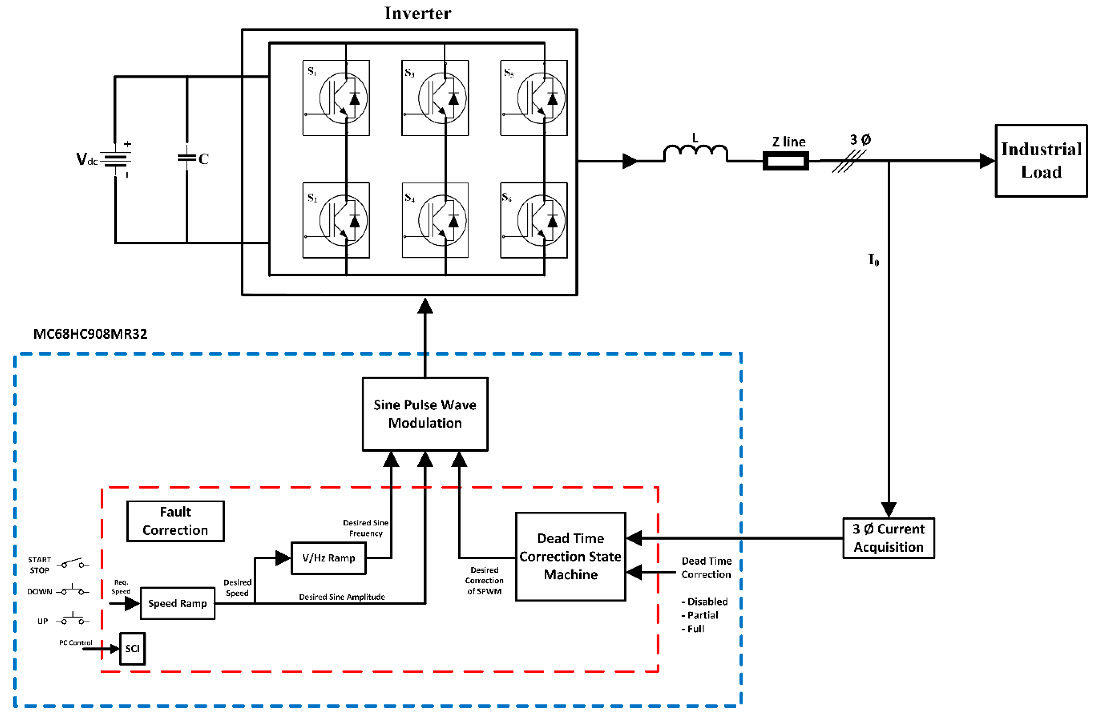
In this paper, the five parameters of power quality have been improved by a novel DTC technique and the consequences of dead time effect on power quality have been eliminated. A schematic of an industrial microgrid with DTC is given in Figure 1. In this figure, industrial motors make up the majority of the industrial microgrid loads. Introducing DTC in power converters can help in curtailing the non-ideal nature of power electronics. The current research attempts to alleviate the effects of dead time on power converter parameters, for instance, curtailing fundamental voltage, distorting current waveforms, phase angle, and third harmonic as well as torque pulsation. The parametric equations for all the parameters are derived for normal scenarios and dead time compensation scenarios. The model is simulated in MATLAB with two different cases and the results, with and without the proposed model application, are drawn.
The article is organized as follows: Section 2 delineates the model structure for power quality enhancement with the DTC technique; Section 3 investigated the proposed DTC method along with the mathematical modeling of this method; Section 4 explains the outcomes of the research work with a discussion on the importance of the research to the field, and Section 5 lists the conclusions derived from the research endeavor.

2. System Modeling

The model of power quality improvement involves the incorporation of high-level pulse width modulation, in this case, IGBT, into the electrical switching system while retaining the switching frequency at 2–15 kHz levels [21]. To cope with the non-ideality in a small delay, called dead time, is inserted in the operation to avoid short circuits. Meanwhile, the dead time causes various parameters deterioration, therefore power quality analysis is carried out which mostly focused on the reduction of the negative consequences of dead time. The proposed method consists of dead time compensation (DTC) strategy for stabilization of 3 phase induction motors in the open-loop system using variable frequency drive (VFD) to govern the speed required for AC motors besides the offsetting of the adverse effects of DTC. A schematic of the proposed model is outlined in Figure 2. It consists of “volt-per-Hz” drive the design of which is delineated in the following. A specially minted control mechanism is applied for maintaining a fixed level of magnetizing current. Additionally, variable stator voltage support is also implemented.
Since dead time is directly proportional to PWM signal output; the increase or decrease of one directly decreases or decreases the other resulting in a closer-to-original voltage pulse. Accordingly, the current study employs two methods for correcting dead time induced distortion: full correction methodology which factors in the phase angle magnitude and initiates a novel s/w for enhanced output; and partial correction methodology which helps the PWM on-chip hardware. At least one of these correction methodologies is pertinent to improve the PWM inverter parameters. The increasing parameters of PWM inverter values used in pair register; need to be kept in check with the help of software. The value is dependent on the transistor and is important for the output voltage in DT. The partial correction method essentially builds the basis for polarity detection, which is helpful in the improvement of load current waveform, the magnitude of fundamental voltage, phase angle, third harmonic distortion, and induction motor parameters such as current waveform, torque pulsation, and speed. Albeit many shortcomings are concomitant with this method; the current settles at zero at the point of disturbance.

3. Proposed Dead Time Compensation Technique

In this section, the proposed dead-time compensation (DTC) method is investigated. First, the DTC for the PWM inverter is performed. Then, the modeling of the proposed DTC technique is introduced.

3.1. Dead-Time Compensation for PWM Inverter

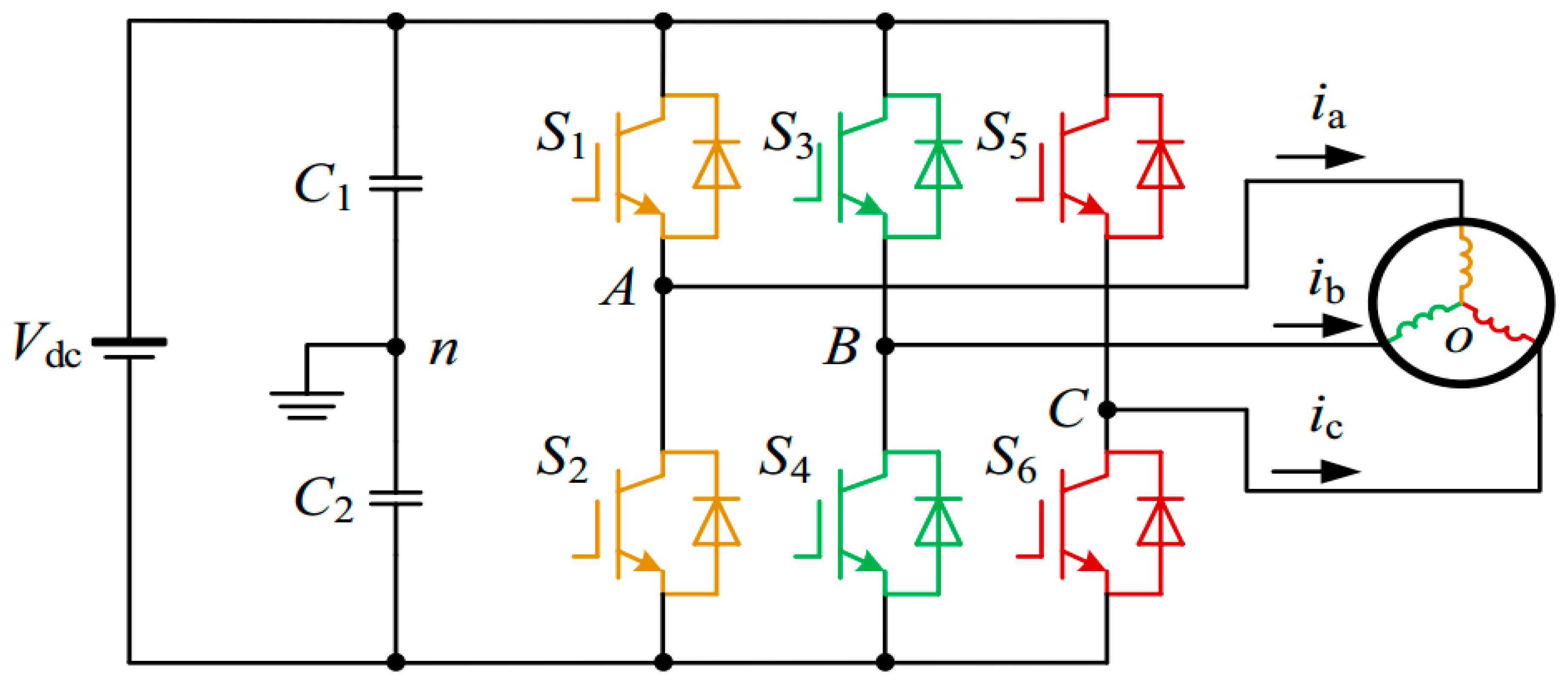
The design of a three-phase voltage-based inverter is given in Figure 3 where ‘n’ and ‘o’ indicate dc link and induction motor neutral points respectively and IGBTs paired with diodes work as switches. As an example, the effect of dead time and forward voltage drops have been examined in phase A leg. The phase A leg contains four different current paths as demonstrated in Figure 3. The forward voltage drop of IGBT is represented as ‘ u c e ’ and that of the anti-diode as ‘ u d ’. From Figure 4, phase A current i a is represented by the dashed line in Figure 4. It is established from Figure 4a,b that when current flows from the inverter to load, i a > 0 and from Figure 4c,d it is evident that i a < 0 for opposite current direction reverses.
Since the delay in the on-off of IGBTs for this study is extremely small in comparison to the dead time, it is considered negligible. In the beginning, the dead time setting is analyzed. The delays between turn on and off of power electronic devices (IGBTs) are considered negligible in this study as they are very small in comparison to the dead time. One switching cycle of sinusoidal pulse width modulation (SPWM) contains two stages of dead time in which power electronic devices remain in the OFF state. Hence, the load current is forced to pass through anti-parallel diodes D1 or D2 (depending on the direction). Current flows through D2 when i a is positive during phase A and is interconnected to the negative terminal as evident from Figure 4b. If i a is negative, current flows through D1 with phase A connection setting shown in Figure 4c.
Forward voltage drop occurs when the switching devices pass load current. When the current is positive, the voltage output at phase A is marginally less than the respective DC linkage voltage. In such instances, the IGBT S1 passes current from the positive linkage or D2 passes current from the negative linkage. Similarly, for negative i a , the voltage output at phase A is marginally greater in comparison to the DC linkage voltage. In this case, positive linkage gets current via D1, and negative linkage via S2. The various permutations of currents flow, and voltage waveforms at different instances are given in Table 1.
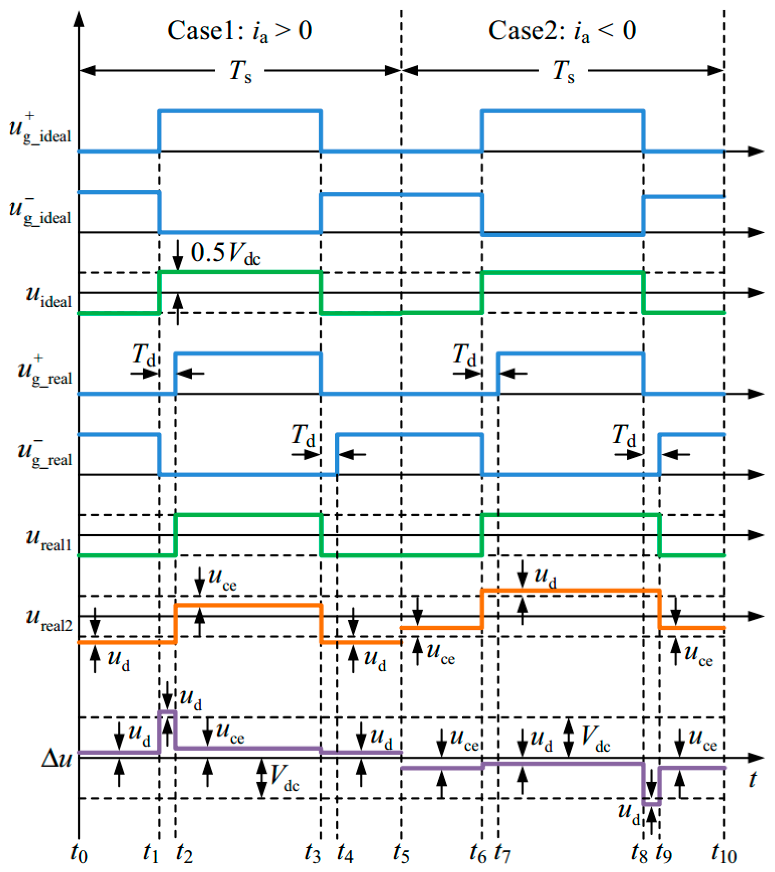
As seen from Table 1 the error voltage is the largest for the time range t 8 t 8 where i a is negative. These analyses for phase A leg can also be applied to three-phase legs. The gate signals and voltage waveforms of phase A as per the pulse generation rule of SPWM are given in Figure 5. It depicts the gate input and dead time incorporated gate input signals for top and bottom switching devices ( u + g , u g ), voltage output ( u i d e a l ), real output voltage incorporating dead time ( u r e a l ), with both dead time and forward voltage drop ( u r e a l 2 ).
Accordingly, the corresponding dead time error is given as the difference between u i d e a l and u i d e a l 2 . Similarly, V d c , T s , and T d indicate the DC linkage voltage, switching period, and dead time respectively. It is evident from the left side of Figure 4 that for negative i a ideal PWM voltage is greater than the actual PWM voltage. In other words, the ideal voltage output will exceed the actual voltage output. The actual o/p voltage will be slightly less when the forward voltage drop is applied. The voltage varies between V d c 2 u c e and V d c 2 u d when the load current is applied to positive and negative terminal respectively. It is evident from Figure 5 that the deviation from ideal behavior is a function of dead time. Additionally, there is a dependence on the current direction; when altered from load to positive terminal, the output is V d c 2 + u d , while changes to V d c 2 + u c e for the opposite current direction.

3.2. Modeling of the Proposed Dead Time Compensation

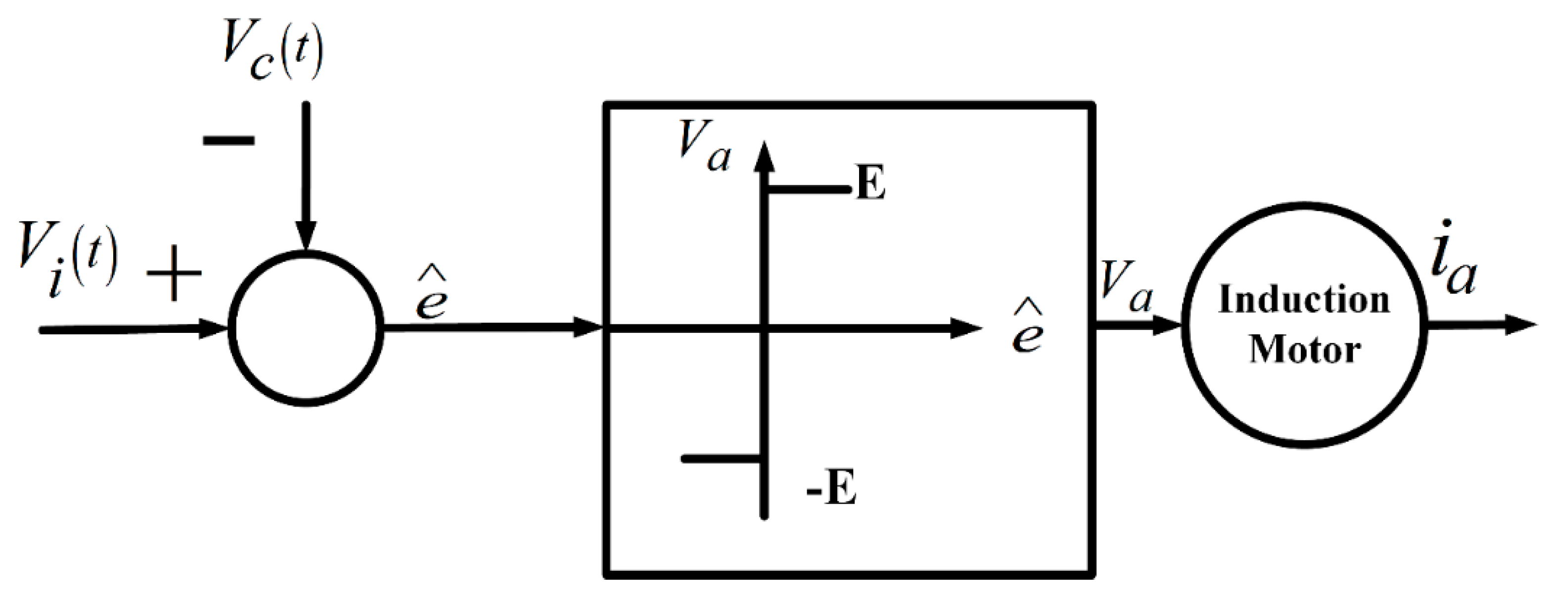
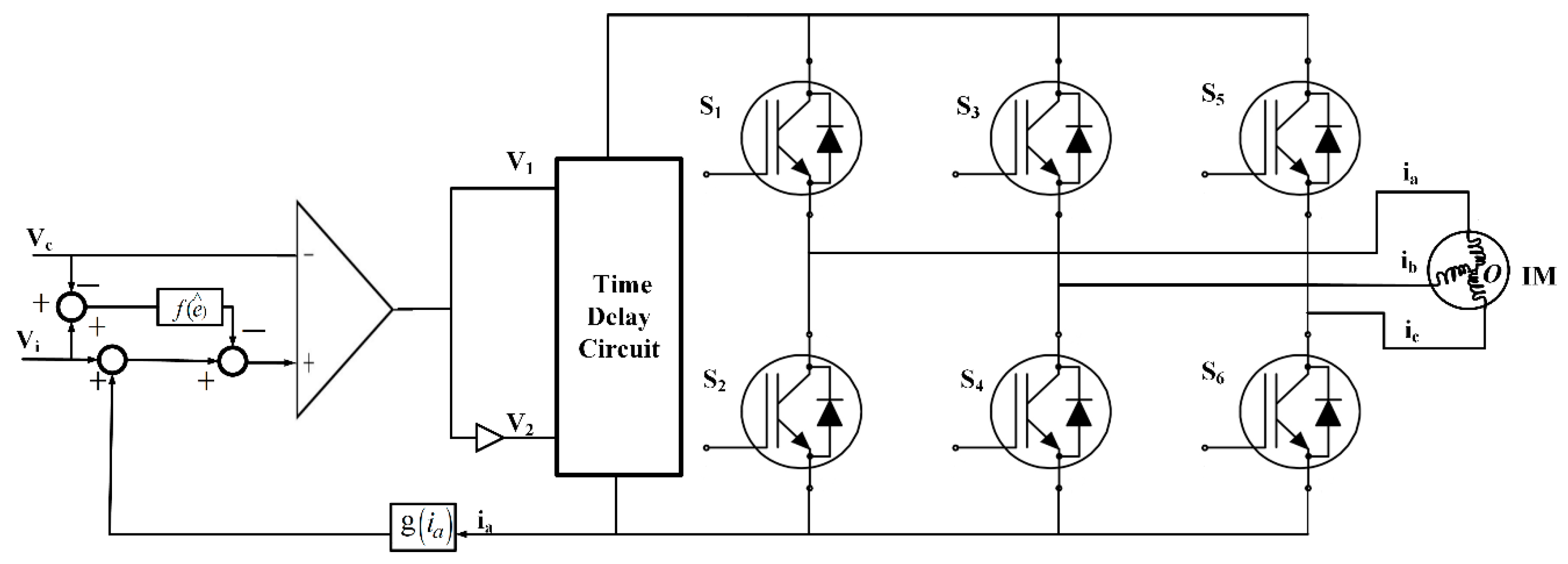
The block diagram for 3-phase idealized PWM inverter is illustrated in Figure 6. The DTC model is schematically presented in Figure 7. The model employs an ideal relay possessing two specifications: memory-less, and nonlinearity. The voltage distortion ε depends on T d the delay time and carrier signal V c ( t ) the slope of the triangular waveform. Take the required signal V i ( t ) is gradually varying as compared to the high-frequency carrier signal C . The ratio ε / T d is equal to 2 V c / ( T c 2 ) the down-slope, the triangular carrier signal V c ( t ) and therefore we have ε = 2 V c T d / ( T c 2 ) = 4 f c V c T d . Where ε represents as voltage distortion, T d is a time delay and f c represents the frequency of the carrier signal.
The desired results can be obtained by setting the deviation ‘ ε ’ to 0 or dead time ‘ T d ’ to 0. Since the inherent objective is to compensate for the dead time, the following derivation further explores the ideal PWM inverter [27].
T e r r = T o f f T o n T d + 2 T c o m
where ‘ T c o m ’ indicates the compensation time when ‘ i a < 0 .
For phase A:
T e r r _ a = S i g n ( i a ) T m a
where
T m a = T o f f T o n T d + 2 T c o m
Sign ( i a ) = { 1             ( i a > 0 ) 1             ( i a < 0 )
When voltage U a is positive for phase A, the switching cycle time duration is T a , and for S 1 , it is T a * . For negative U a , the switching cycle time duration is T a for phase A, and for S 4 it is T a * .
Correspondingly the relation between effective time ( T a ) and commanded time ( T a * ) comes out to be [21]:
T a = T a * + S i g n ( i a ) T m a  
Similarly, for Phase B and C the same quantities are given as:
T b = T b * + S i g n ( i b ) T m b  
T c = T c * + S i g n ( i c ) T m c
where IGBTs S 3 and S 1 remain turned on and off respectively for (1) to (7). However, at the neutral point when fundamental voltage is balanced:
V d c 1 = V d c 2 = V d c 2 2
when i a > 0 :
V a o = V d c 2 2 V c e ( w h e n   S a = 1 )
V a o = V d V c e ( w h e n   S a = 0 )
V a o = V d c 2 + 2 V c e ( w h e n   S a = 1 )
when i a < 0 ;
V a o = V d c 2 + 2 V d ( w h e n   S a = 1 )  
V a o = V d + V c e ( w h e n   S a = 0 )
V a o = V d c 2 + 2 V c ( w h e n   S a = 1 )
Supposing no change in the direction of current, (8)–(13) gives:
V a o = S a ( 1 2 V d c + V d V c e ) S i g n ( i a ) ( V c e + V d )  
When voltage drop increases with respect to current:
V c e = V c e o + r c e | i a |
V d = V d o + r r d | i a |  
Combining (15) and (16) with (14) gives:
V a o = S a ( 1 2 V d c + V d V c e ) S i g n ( i a ) ( V c e + V d )  
As per volt-second balance theorem:
S a = [ T a * + T m a S i g n ( i a ) T s ] S i g n ( U a _ r e f )
V a = [ T a * + T m a S i g n ( i a ) T s ] ( 1 2 V d c + V d V c e ) S i g n ( U a _ r e f ) ( V c e o + V d o ) S i g n ( i a ) ( r c e + r d ) i a
Now for phase b and c:
V b = [ T b * + T m b S i g n ( i b ) T s ] ( 1 2 V d c + V d V c e ) S i g n ( U b _ r e f ) ( V c e o + V d o ) S i g n ( i b ) ( r c e + r d ) i b
V c = [ T c * + T m a S i g n ( i c ) T s ] ( 1 2 V d c + V d V c e ) S i g n ( U c _ r e f ) ( V c e o + V d o ) S i g n ( i c ) ( r c e + r d ) i c
Balanced load for three-phase loads is indicated as:
V a + V b + V c = 0  
i a + i b + i c = 0
{ V a = V a o + V o V b = V b o + V o V c = V c o + V o
Hence, the schematic illustration of the PWM inverter shown in Figure 3 is thus transformed into the final DTC model schematically represented in Figure 8.
Subsequently, the control block of the upper section ( ( ε 2 ) s i g n ( i a ) ) is canceled out with a feedback block ( g ( i a ) = ( ε 2 ) s i g n ( i a ) a). The Feed-forward f(ê) method is employed for dealing with hysteresis. The hysteresis compensation block as given in Figure 7 is utilized. To achieve the characteristics of an ideal relay, transfer features such as m, V a are used. Figure 7 also gives a representation of the dead time feedback blocks g ( i a ) , and feed-forward block f ( ê ) of the SPWM inverter model. Owing to the inherent phase lag the feed-forward compensation cannot be ignored. At this stage, the DTC technique can be applied to the 3-phase PWM inverter, an example of which has been demonstrated in Figure 3.
The compensation of dead time blocks g ( i a ) (feedback) and f ( ê ) (feedforward) of the 3 phase SPWM inverter model is presented in Figure 7 schematically. Due to an inherent phase lag, the f(ê) (feed-forward compensation) cannot be ignored. Just now at this stage, the DTC technique is ready to be applied on 3-phase PWM inverter for practical implementation which is presented in Figure 3.
Furthermore, before the dead time compensation method the equation has the following shape:
e = [ V i ( t ) ] V c ( t )
After converting the deviation, ε , to phase voltage, V a ; adjusting T d and ε equal to zero; eliminating the factor ( ε 2 ) s i g n ( i a ) through feedback factor g ( i a ) = ( ε 2 ) s i g n ( i a ) application; and applying for the compensation through feedforward for dealing with the inherent phase angle.
It is pertinent that the voltage control signal V i ( t ) in (25) is equal to [ V i ( t ) f ( e ^ ) + g ( i a ) ] and Equation (25) becomes:
e = [ V i ( t ) f ( e ^ ) + g ( i a ) ] V c ( t )  
where   e ^ = V i V c and f ( ê ) and g ( i a ) are nonlinear functions.

4. Results and Discussion

Following the mathematical modeling, the proposed dead-time compensation model was simulated using MATLAB/Simulink for validation of the method. The V / f strategy was employed for system control. Since the compensation strategy only depends on the characteristics of the power devices, a three-phase Y-connected symmetrical RL load was deployed at the output terminal of the inverter. The key parameters used in the simulation are listed in Table 2 while the important characteristics of the industrial motor are given in Table 3. The simulation time is kept twice the fundamental period to avoid imprecise results and surplus data; otherwise, the simulation may stop due to computer memory exhaustion.
Dead-time distortion correction algorithms are a useful tool for adjusting PWM relevant to the actual polarity of phase current. The PWM control signal is extended by the addition of dead time, to match the actual pulse with the desired values, when the voltage pulse is shortened. Contrarily, for prolonged voltage pulse by dead time, the PWM signal is reduced by an equivalent time, leading to a match between the actual and desired voltage pulse. Resultantly an actual voltage signal equal to the desired signal is achieved, along with a sinusoidal phase current.

4.1. Impact of Dead Time on Load Current Waveform

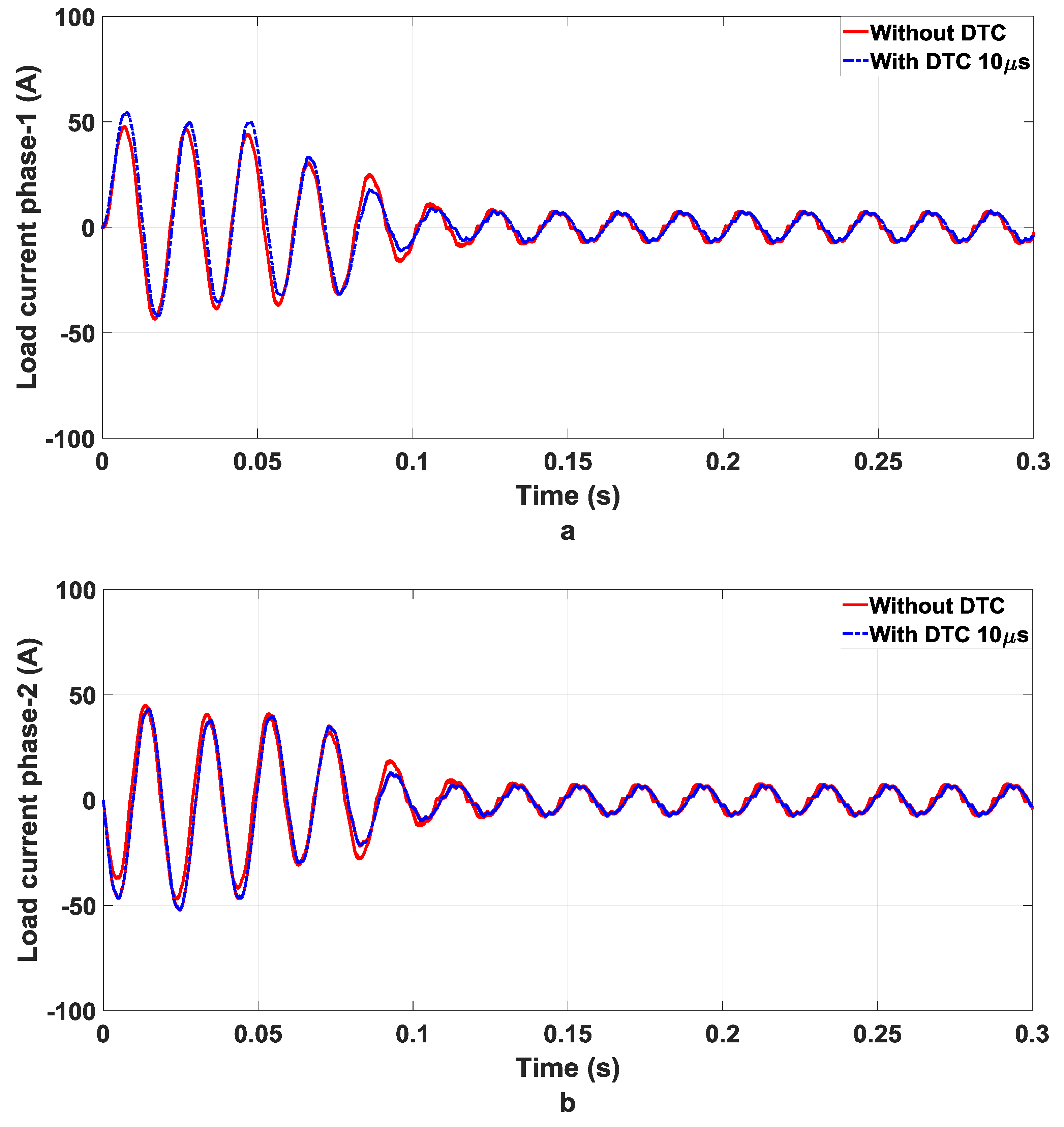
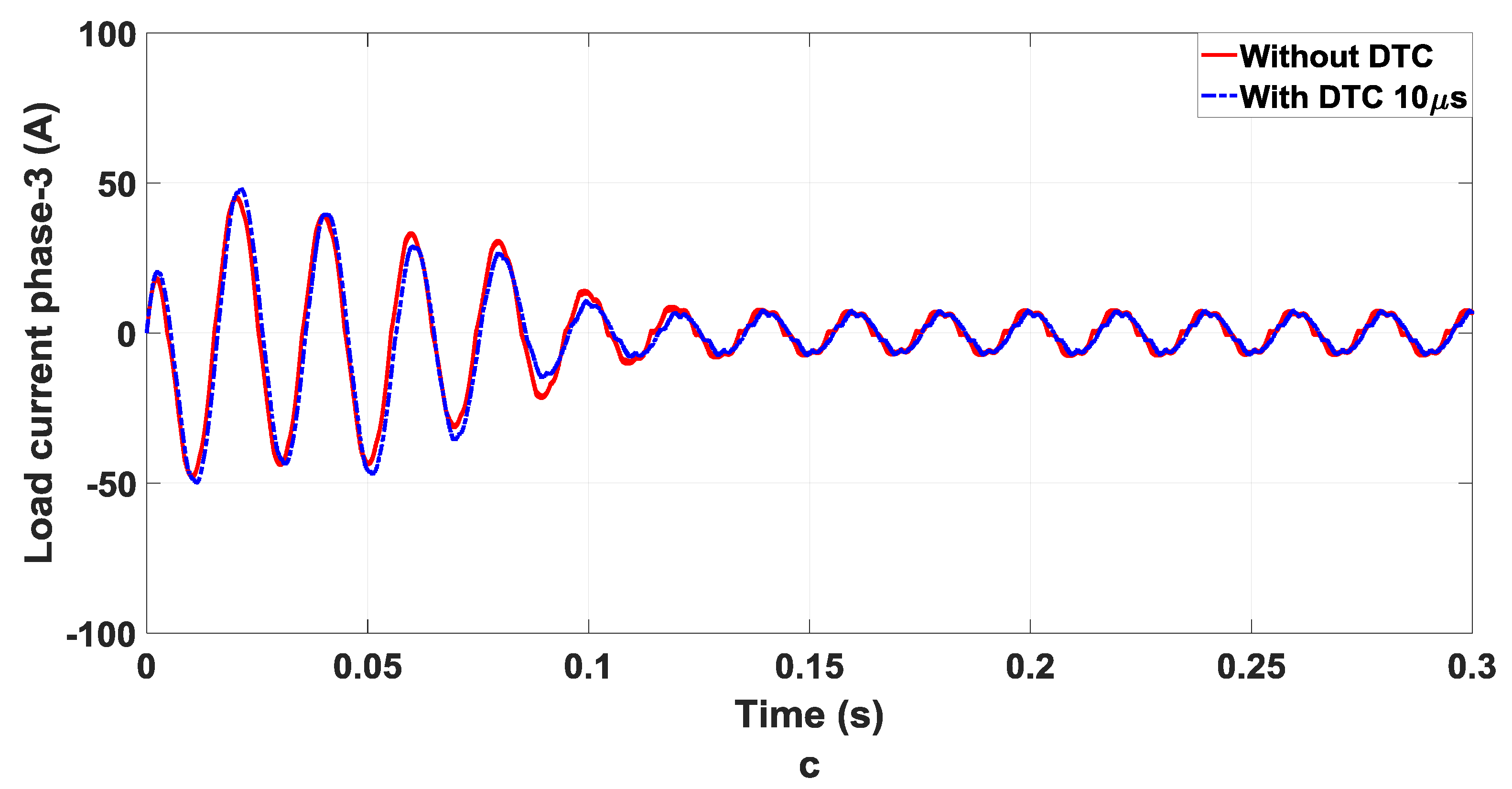
Without the dead time compensation and the proposed dead time compensation method, when the fundamental frequency f1 is 5 Hz, the load current waveform is substantially improved. The amplitude of the current waveform is increased and distortion is reduced significantly. The current waveform is almost the same as the ideal current waveform. The provision for the mandatory delay in switching signals in IGBTs to accommodate dead time can induce undesirable sub-harmonics, subsequently causing deviation in load current as illustrated in Figure 9. The proposed DTC compensates the distortions to make the signal more sinusoidal as shown in Figure 10.

4.2. Total Harmonics and Individual Harmonics Distortions Calculation by FFT Analysis

The third harmonic distortion is the main problem due to the non-ideal characteristics of power converters. By nature, ‘each regularly distorted waveform may be defined as a number of pure sine waves in which the frequency of each sinusoid is an integer multiple of the fundamental frequency of the distorted wave. The sum of the sinusoids is referred to as the “Fourier series.” In recent years, they have also concentrated on the harmonic distortion of the power field.
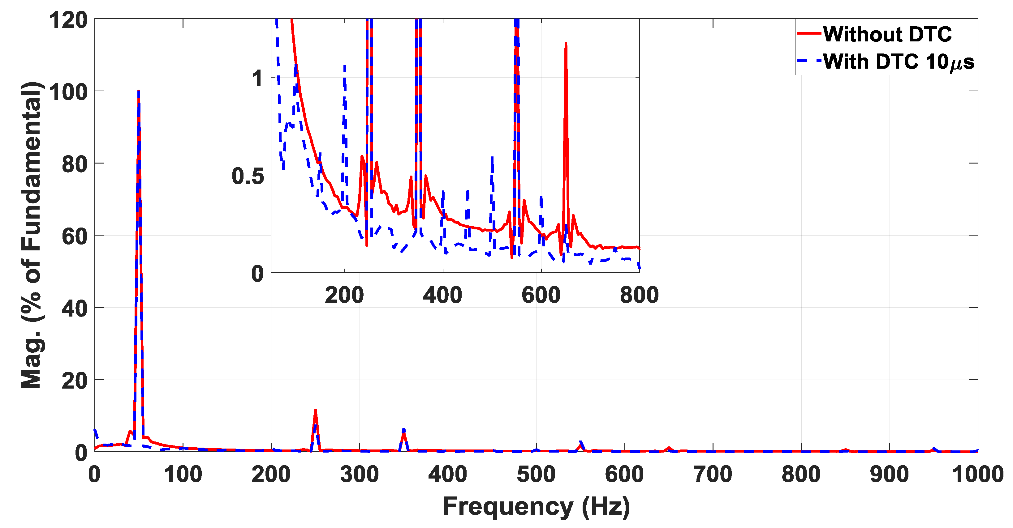
Dead-time is unavoidable in inverter circuitry as it prevents short-circuiting. However, it comes with the side effect of total harmonic distortion, thus necessitating DTC. The proposed DTC can alleviate the side effects. As can be seen from Figure 10, the third harmonic distortion is 16.26% without DTC. However, after the application of the novel DTC, the distortion is mitigated by 3.77% to 12.49%, as presented in Table 4. This improvement of almost 4% will be instrumental for the health of the motors operating in industrial load.
Individual harmonic distortion (IHD) represents the relation between the root mean square (RMS) value of the fundamental (RMS) value of the individual harmonics in Equation (29) [28]:
I H D n = I n / I 1
For third harmonic, n is represented by 3. From Figure 10, the RMS of the fundamental current is equal to 100. Also, the RMS of the third harmonic current without DTC is 11.615 A and with DTC is 7.475 A. Therefore, I H D 3 = 11.615   / 100 100 = 11.615   without DTC and I H D 3 = 7.475 with DTC.

4.3. Improvement in Fundamental Voltage Magnitude and Phase Angle

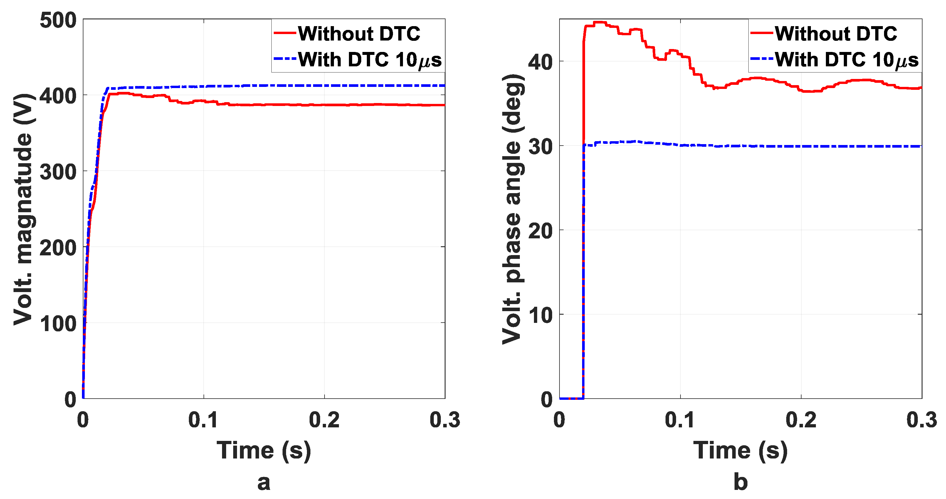
Dead-time induces certain drawbacks in the power electronic circuitry such as a decrease in fundamental voltage and distortion of other parameters. These effects can be effectively coped with through the incorporation of the proposed DTC. The fundamental voltage magnitude can be restored, and the harmonics minimized. Figure 11a for dead time 10 μ s presents the fundamental voltage magnitude in the absence of DTC and presents the same parameter after DTC, respectively. It is evident that the fundamental voltage has significantly improved as a result of the application of the proposed DTC technique.
Phase angle distortion is also a downside of dead time. However, an efficient DTC strategy can handle this drawback to a certain degree. The proposed DTC model can achieve significant improvements in this domain as well. Figure 11b for dead time 10 μ s shows the phase angles distortion pre and posts using the DTC technique respectively. It is vividly evident from these figures that the phase angle distortion has been significantly reduced through the application of the proposed DTC technique.

4.4. Improvement in Power Quality Parameters of Induction Motor

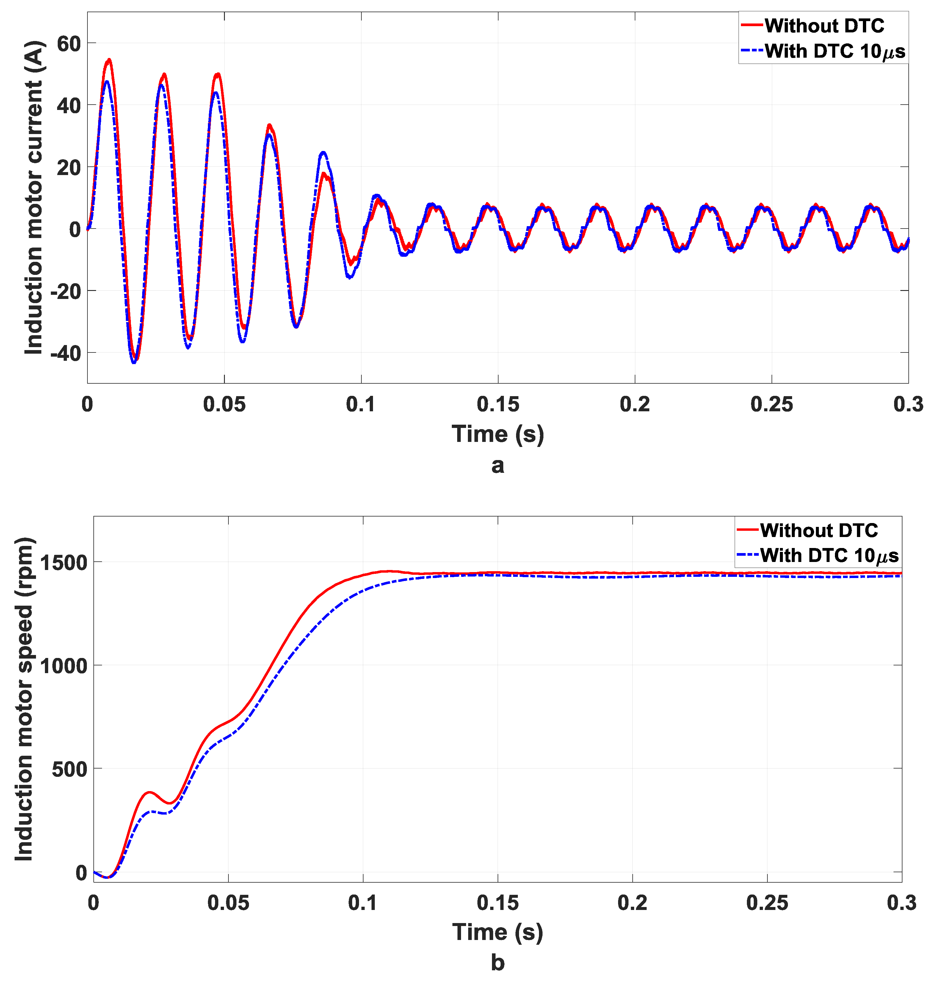
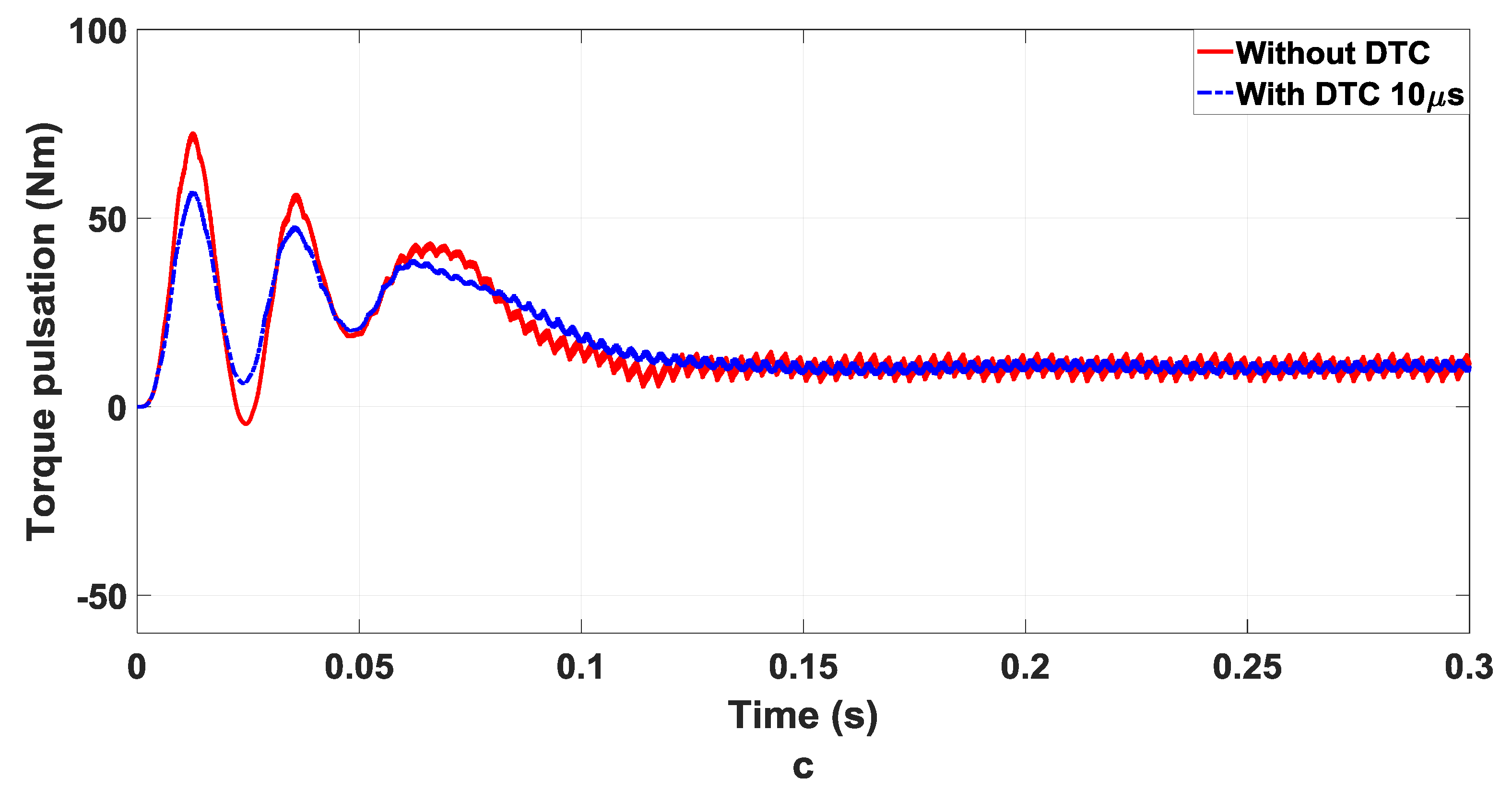
The induction motors are major energy-using equipment, any issues with their smooth operation are extremely significant. The unavoidable delay in signal switching can cause sub-harmonics leading to waveform distortion in the current signal. Additionally, it can also lead to pulsation in torque, and reduction in the rotational speed of the motor, manifesting in heat dissipation from the motors. These distortions and the concomitant damages can be significantly reduced by employing an efficient DTC technique. The DTC technique can restore the current to one looking more like the sinusoidal curve which entails the remedy of the aforementioned drawbacks in motor performance. DTC insertion in the inverter circuitry has been shown to mitigate the harmonic distortion and load torque pulsation. Furthermore, DTC can lead to practical improvements in motor performance such as smooth operation, limited torque ripples, low noise, and enhance efficiency in operation due to lower harmonic losses.
The proposed DTC technique has been applied to the inverter circuit with the harmonic distortion mentioned above. Figure 12a–c show the improvement in the current waveform distortion, motor speed, and torque pulsation respectively. In Figure 12a–c, using DTC application shows better performance in comparison with using DTC application for the motor speed and the torque pulsation, respectively. The left side of these figures represents these parameters before the application of DTC, while the right sides represent the post DTC parameters’ behavior.

4.5. Case 2: Dead-Time 1 μ sec and Switching Frequency 1 kHz

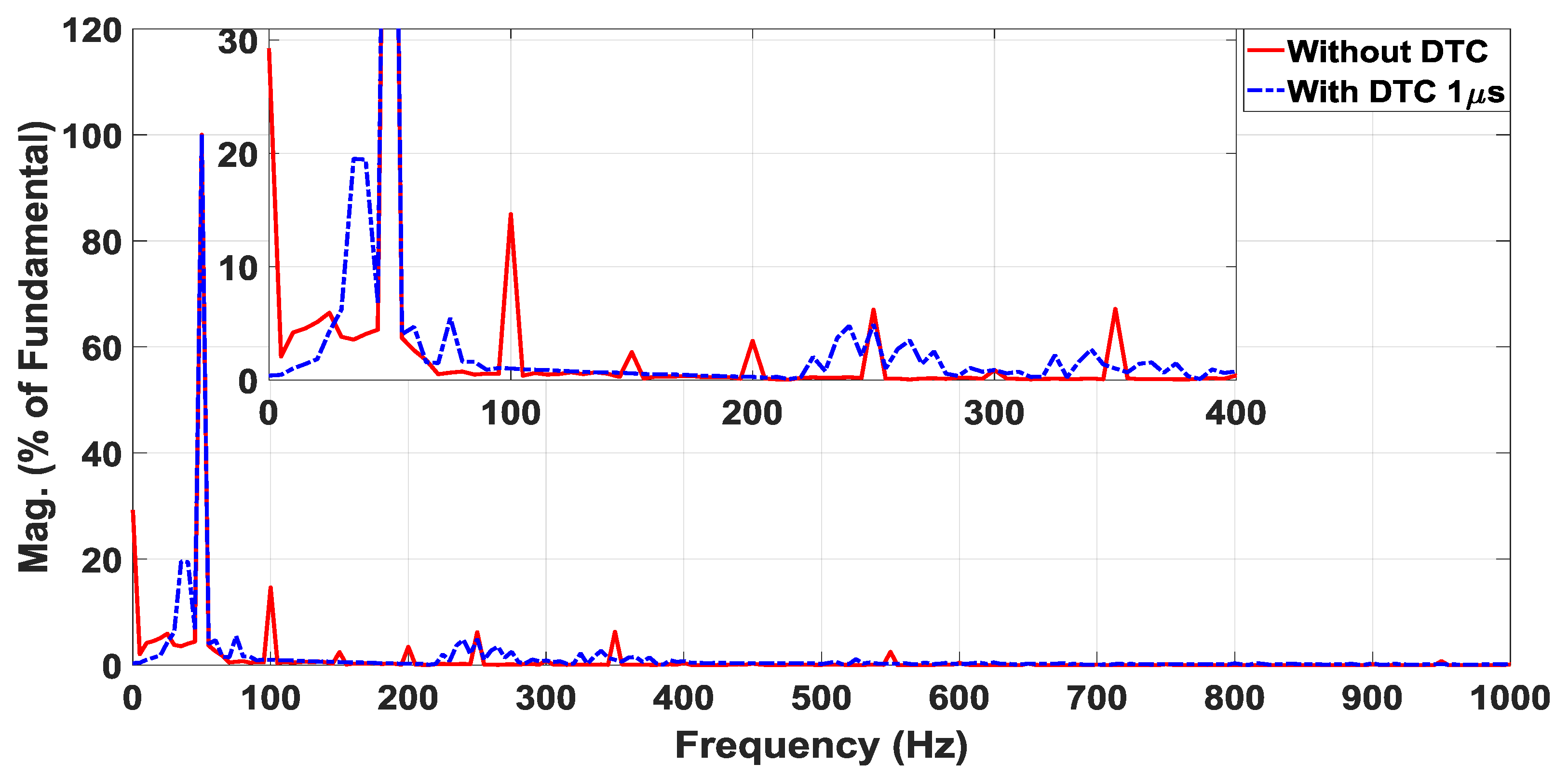
In case 2, the studies show that the current magnitude of the harmonics is the same, while the distortion factors are different due to time increasing as shown in Figure 13. If we take 1 micro-second, as shown in Figure 13, the third harmonic distortion without DTC is 16.26 percent. Moreover, after the implementation of the proposed DTC, method the distortion is reduced from 18.36% to 10.20%, as seen in Table 5. For the quality of power in industrial loads, an average increase of almost 8% is important.
From Figure 13, the RMS of the fundamental current is equal to 100. Also, the RMS of the third harmonic current without DTC is 15.707   A and with DTC is 10.295 A. Therefore, I H D 3 = 29.2759 / 100 100 = 29.2759 %   without DTC and I H D 3 = 14.645 % with DTC.
Similarly, the fundamental voltage magnitude may be recovered in case 2 and the harmonics reduced as shown in Figure 14a. Figure 14a explicitly indicates the voltage magnitude in the presence of the DTC and also displays the same parameter before the DTC when time is 1 microsecond. It is clear that the voltage magnitude has dramatically changed as a result of the implementation of the new DTC methodology.
In fact, the distortion of the phase angle in case 2 is also increased due to dead-time effects. However, if we take 1 micro-second, an effective DTC strategy will deal with this problem to some large extent. Figure 14b demonstrates the before and after the distorted phase angles of voltage magnitude by using the DTC methodology, respectively. It is clear from this figure that the distortion of the phase angle was greatly decreased by the implementation of the new DTC strategy.
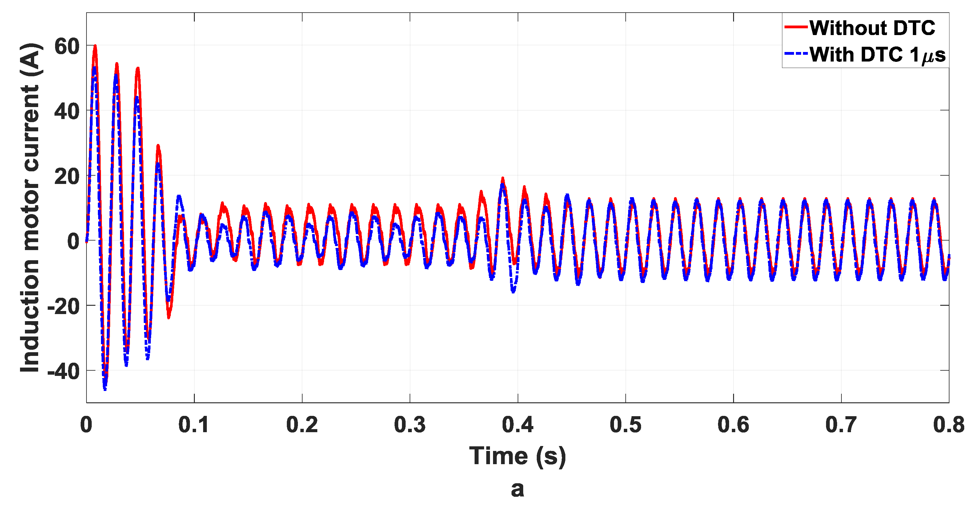
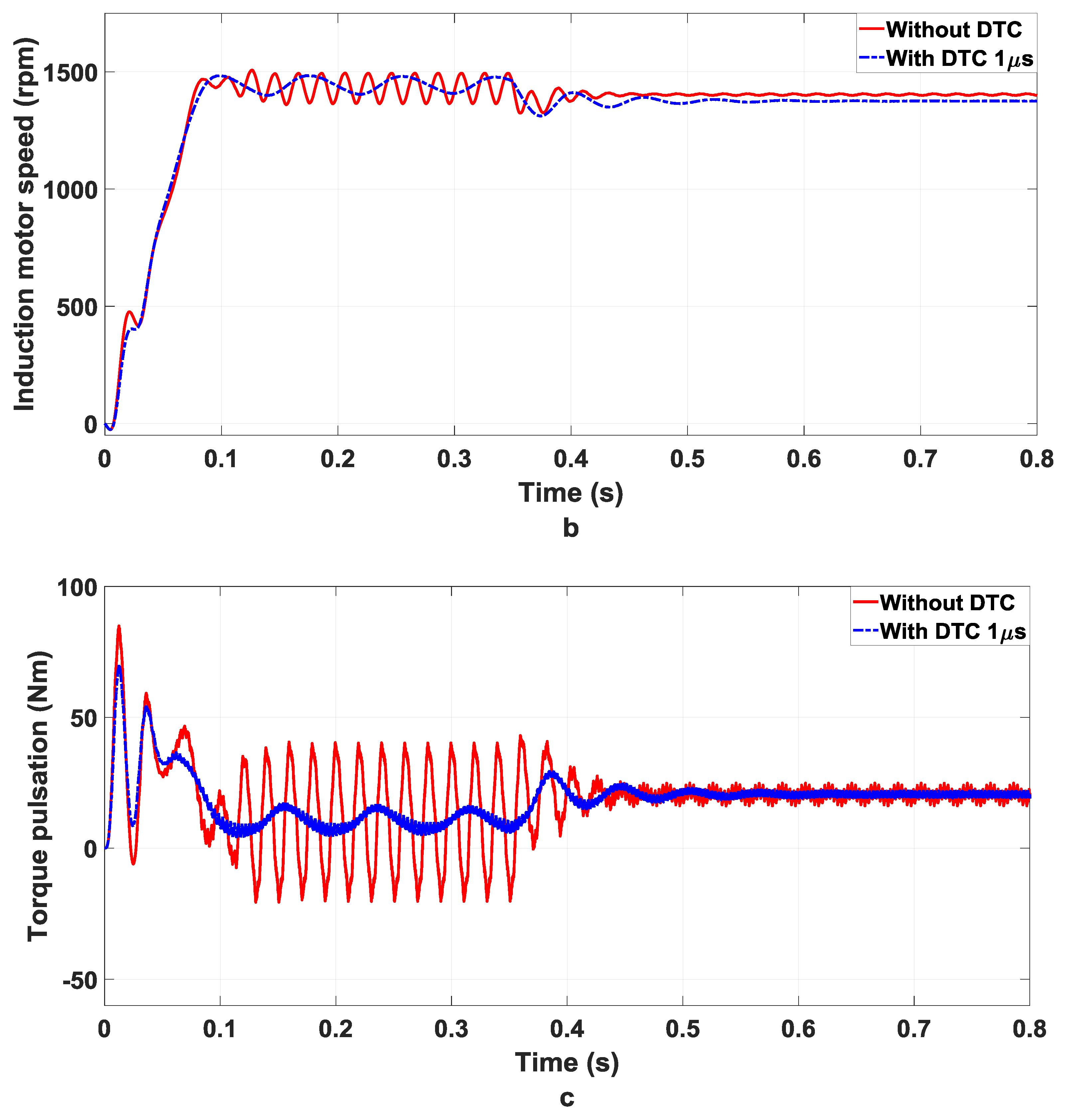
In case 2 while the dead time is changed from 10 to 1 micro-seconds, the DTC incorporation in the inverter circuit is shown to reduce the total harmonic distortions and also torque pulsation as shown in Figure 15a. In addition, DTC will lead to realistic changes in an induction motor performance, along with the smooth operation, low noise, minimal torque ripples, and increased operating efficiency due to the lower harmonic losses. Figure 15a–c demonstrate the increase in current waveform quality, induction motor speed, and also torque pulsation, collectively.

5. Conclusions

The research endeavor successfully models and implements a novel dead time technique rooted in dead time compensation for enhancing the power quality parameters. The overall efficiency improvement of power converters has been achieved from cumulative improvements in several power quality parameters such as sinusoidal load current, phase angle, fundamental voltage magnitude, harmonic distortion. Further, the mitigation in a motor operation like torque pulsation smoothening, current waveform restoration, and speed enhancement are also enhanced. The parametric equations for all the parameters are derived for normal scenarios and dead time compensation scenarios. The model is simulated in MATLAB with two different cases and the results, with and without the proposed model application, are drawn. Finally, two separate case studies of the performance relative to the pre-model and major changes in all dimensions of the power quality parameters and the output of the power converters deficiency are found by the implementation of the dead time compensation technique. The proposed DTC results in significant improvement in the following parameters as exhibited in Figure 9, Figure 10, Figure 11, Figure 12, Figure 13, Figure 14 and Figure 15:
(a)
Sinusoidal load current waveform has been achieved by applying dead time compensation, leading to the removal of distortions accruing from harmonics
(b)
Fundamental voltage magnitude has been significantly restored through the proposed DTC implementation.
(c)
The phase angle has been improved through the proposed DTC strategy. Additionally, the third harmonic distortion has been significantly alleviated 3.77%, through the proposed DTC strategy in Case 1 and 3.04% in Case 2.
(d)
Significant improvements have been achieved in the induction motor parameters post the DTC strategy application. Parameters like torque pulsation, speed, and THD which cause hindrance in smooth motor operation have been demonstrably improved through the novel technique.

Author Contributions

Conceptualization, S.I.; Data curation, M.A.A., M.A., and S.A.A.R.; Formal analysis, M.U.J., M.A.A., M.A., and N.A.S.; Funding acquisition, A.X.; Investigation, H.U.R., S.S., S.A.A.R., and N.A.S.; Methodology, S.I. and A.X.; Project administration, A.X.; Resources, A.X.; Software, S.I.; Supervision, A.X.; Validation, M.U.J., and M.A.A.; Visualization, H.U.R., and S.S.; Writing—original draft, S.I.; Writing—review & editing, A.X., M.U.J., and M.A.A. All authors have read and agreed to the published version of the manuscript.

Funding

This work was supported by the 2016 national key R & D program of China to support low-carbon Winter Olympics of integrated smart grid demonstration project (2016YFB0900500) and Beijing Natural Science Foundation (3182037). The Fundamental Research Funds for the Central Universities under Grant 2019QN041.

Conflicts of Interest

The authors declare no conflict of interest.

References

  1. Nejabatkhah, F.; Li, Y.W.; Tian, H. Power quality control of smart hybrid AC/DC microgrids: An overview. IEEE Access 2019, 7, 52295–52318. [Google Scholar] [CrossRef]
  2. Aziz, T.; Ahmed, M.; Nahid-Al-Masood. Investigation of harmonic distortions in photovoltaic integrated industrial microgrid. J. Renew. Sustain. Energy 2018, 10, 053507. [Google Scholar] [CrossRef]
  3. Abdelbaky, M.A.; Liu, X.; Jiang, D. Design and implementation of partial offline fuzzy model-predictive pitch controller for large-scale wind-turbines. Renew. Energy 2020, 145, 981–996. [Google Scholar] [CrossRef]
  4. Kong, X.; Ma, L.; Liu, X.; Abdelbaky, M.A.; Wu, Q. Wind Turbine Control Using Nonlinear Economic Model Predictive Control over All Operating Regions. Energies 2020, 13, 184. [Google Scholar] [CrossRef] [Green Version]
  5. Iqbal, S.; Xin, A.; Jan, M.U.; Salman, S.; Zaki, A.u.M.; Rehman, H.U.; Shinwari, M.F.; Abdelbaky, M.A. V2G Strategy for Primary Frequency Control of an Industrial Microgrid Considering the Charging Station Operator. Electronics 2020, 9, 549. [Google Scholar] [CrossRef] [Green Version]
  6. Gandoman, F.H.; Ahmadi, A.; Sharaf, A.M.; Siano, P.; Pou, J.; Hredzak, B.; Agelidis, V.G. Review of FACTS technologies and applications for power quality in smart grids with renewable energy systems. Renew. Sustain. Energy Rev. 2018, 82, 502–514. [Google Scholar] [CrossRef]
  7. Belov, V.; Butkina, A.; Bolschikov, F.; Leisner, P.; Belov, I. Power quality and EMC solutions in micro grids with energy-trading capability. In Proceedings of the 2014 International Symposium on Electromagnetic Compatibility, Gothenburg, Sweden, 1–4 September 2014; pp. 1203–1208. [Google Scholar]
  8. Standard IEC 61000-2-2. Electromagnetic Compatibility (EMC)-Part 2-2: Environment-Compatibility Levels for Low-Frequency Conducted Disturbances and Signalling in Public Low-Voltage Power Supply Systems; IEC: Geneva, Switzerland, 2002. [Google Scholar]
  9. Dong, H.; Yuan, S.; Han, Z.; Ding, X.; Ma, S.; Han, X. A comprehensive strategy for power quality improvement of multi-inverter-based microgrid with mixed loads. IEEE Access 2018, 6, 30903–30916. [Google Scholar] [CrossRef]
  10. Elbasuony, G.S.; Aleem, S.H.A.; Ibrahim, A.M.; Sharaf, A.M. A unified index for power quality evaluation in distributed generation systems. Energy 2018, 149, 607–622. [Google Scholar] [CrossRef]
  11. Martinenas, S.; Knezović, K.; Marinelli, M. Management of power quality issues in low voltage networks using electric vehicles: Experimental validation. IEEE Trans. Power Deliv. 2016, 32, 971–979. [Google Scholar] [CrossRef] [Green Version]
  12. Szczesniak, P. Challenges and design requirements for industrial applications of AC/AC power converters without DC-link. Energies 2019, 12, 1581. [Google Scholar] [CrossRef] [Green Version]
  13. Guha, A.; Narayanan, G. Small-signal stability analysis of an open-loop induction motor drive including the effect of inverter deadtime. IEEE Trans. Ind. Appl. 2015, 52, 242–253. [Google Scholar] [CrossRef]
  14. Guha, A.; Narayanan, G. Impact of undercompensation and overcompensation of dead-time effect on small-signal stability of induction motor drive. IEEE Trans. Ind. Appl. 2018, 54, 6027–6041. [Google Scholar] [CrossRef]
  15. Lin, Y.-K.; Lai, Y.-S. Dead-time elimination of PWM-controlled inverter/converter without separate power sources for current polarity detection circuit. IEEE Trans. Ind. Electron. 2009, 56, 2121–2127. [Google Scholar]
  16. Dafang, W.; Bowen, Y.; Cheng, Z.; Chuanwei, Z. A feedback-type phase voltage compensation strategy based on phase current reconstruction for ACIM drives. IEEE Trans. Power Electron. 2013, 29, 5031–5043. [Google Scholar] [CrossRef]
  17. Shen, Z.; Jiang, D. Dead-time effect compensation method based on current ripple prediction for voltage-source inverters. IEEE Trans. Power Electron. 2018, 34, 971–983. [Google Scholar] [CrossRef]
  18. Lim, J.-W.; Bu, H.; Cho, Y. Novel Dead-Time Compensation Strategy for Wide Current Range in a Three-Phase Inverter. Electronics 2019, 8, 92. [Google Scholar] [CrossRef] [Green Version]
  19. Iqbal, S.; Xin, A.; Jan, M.U.; Rehman, H.; Salman, S.; Rizvi, S.A.A. Improvement in the Efficiency of Inverter Involved in Microgrid. In Proceedings of the 2018 2nd IEEE Conference on Energy Internet and Energy System Integration (EI2), Beijing, China, 20–22 October 2018; pp. 1–5. [Google Scholar]
  20. Huang, Z.-L.; Jiang, Z.; Li, Z.-H. Dead-time Compensation Strategy of Three Level Inverter Based on FFT. DEStech Trans. Eng. Technol. Res. 2019. [Google Scholar] [CrossRef]
  21. Zhao, L.; Song, W.; Feng, J. A Compensation Method of Dead-Time and Forward Voltage Drop for Inverter Operating at Low Frequency. J. Electr. Eng. Technol. 2019, 14, 781–794. [Google Scholar] [CrossRef]
  22. Ji, Y.; Yang, Y.; Zhou, J.; Ding, H.; Guo, X.; Padmanaban, S. Control strategies of mitigating dead-time effect on power converters: An overview. Electronics 2019, 8, 196. [Google Scholar] [CrossRef] [Green Version]
  23. Mousavi, S.Y.M.; Jalilian, A.; Savaghebi, M. Voltage unbalance compensation by a grid connected inverter using virtual impedance and admittance control loops. In Proceedings of the 2018 9th Annual Power Electronics, Drives Systems and Technologies Conference (PEDSTC), Tehran, Iran, 13–15 February 2018; pp. 174–179. [Google Scholar]
  24. Wang, D.; Peng, F.; Ye, J.; Yang, Y.; Emadi, A. Dead-time effect analysis of a three-phase dual-active bridge DC/DC converter. IET Power Electron. 2017, 11, 984–994. [Google Scholar] [CrossRef]
  25. Kim, D.-Y.; Won, I.-K.; Lee, J.-H.; Won, C.-Y. Efficiency improvement of synchronous boost converter with dead time control for fuel cell-battery hybrid system. J. Electr. Eng. Technol. 2017, 12, 1891–1901. [Google Scholar]
  26. Mora, A.; Juliet, J.; Santander, A.; Lezana, P. Dead-time and semiconductor voltage drop compensation for cascaded H-bridge converters. IEEE Trans. Ind. Electron. 2016, 63, 7833–7842. [Google Scholar] [CrossRef]
  27. Guo, J.; Gong, X.; Zhao, F.; Wen, X. A novel dead-time compensation strategy of three-level inverter. In Proceedings of the 2014 IEEE Conference and Expo Transportation Electrification Asia-Pacific (ITEC Asia-Pacific), Beijing, China, 31 August–3 September 2014; pp. 1–5. [Google Scholar]
  28. Sankaran, C. Power Quality; CRC press: Boca Raton, FL, USA, 2017. [Google Scholar]
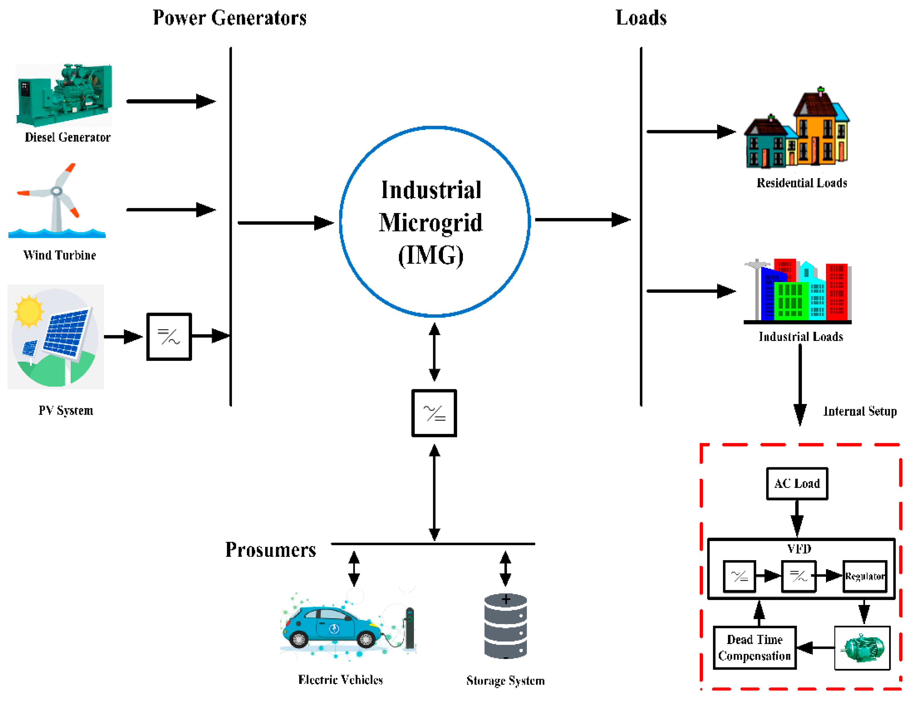
Figure 1. Conceptual view of an Industrial Microgrid.
Applsci 10 03121 g001
Figure 2. Model structure with dead-time compensation.
Applsci 10 03121 g002
Figure 3. Two-level inverter-motor system [21].
Applsci 10 03121 g003
Figure 4. Analysis of different current flow paths of phase A. (a) When i_a>0 from D1 (b) When i_a>0 from D2 (c) When i_a<0 from D1 (d) When i_a<0 from D2 [21].
Applsci 10 03121 g004
Figure 5. Illustration of voltage waveforms and gate signals [21].
Applsci 10 03121 g005
Figure 6. Block diagram for 3-phase idealized pulse width modulation (PWM) inverter.
Applsci 10 03121 g006
Figure 7. Proposed model for the (DTC) method.
Applsci 10 03121 g007
Figure 8. Three-phase SPWM inverter with the proposed DTC method.
Applsci 10 03121 g008
Figure 9. Load current with/without DTC (a) phase 1 (b) phase 2 (c) phase 3.
Applsci 10 03121 g009aApplsci 10 03121 g009b
Figure 10. Calculation of total harmonic distortion (THD) without and with DTC.
Applsci 10 03121 g010
Figure 11. Without/with 10 μ s DTC (a) fundamental voltage ( V a ) magnitude (b) fundamental voltage ( V a ) phase angle.
Applsci 10 03121 g011
Figure 12. Without/with 10 μ s DTC (a) induction motor current (b) speed of induction motor (c) Torque pulsation.
Applsci 10 03121 g012aApplsci 10 03121 g012b
Figure 13. Calculation of total harmonic distortion (THD) without and with DTC.
Applsci 10 03121 g013
Figure 14. With/without DTC (a) fundamental voltage ( V a ) magnitude (b) fundamental voltage ( V a ) phase angle.
Applsci 10 03121 g014
Figure 15. Without/with 1 μ s DTC (a) induction motor current (b) speed of induction motor (c) Torque pulsation.
Applsci 10 03121 g015aApplsci 10 03121 g015b
Table 1. The error between the ideal voltage and the actual voltage.
Time (T)Ideal O/P Voltage/Actual VoltageIdeal O/P VoltageActual O/P VoltageDead-Time Error
t 0 t 1 D 2 / D 2 V d c / 2 V d c / 2 u d u d
t 1 t 2 S 1 / D 2 V d c / 2 V d c / 2 u d V d c + u d
t 2 t 3 S 1 / S 1 V d c / 2 V d c / 2 u c e u c e
t 3 4 D 2 / D 2 V d c / 2 V d c / 2 u d u d
t 4 t 5 D 2 / D 2 V d c / 2 V d c / 2 u d u d
t 5 t 6 S 2 / S 2 V d c / 2 V d c / 2 + u c e u c e
t 6 t 7 D 1 / D 1 V d c / 2 V d c / 2 + u d u d
t 7 t 8 D 1 / D 1 V d c / 2 V d c / 2 + u d u d
t 8 t 9 S 2 / D 1 V d c / 2 V d c / 2 + u d V d c u d
t 9 t 10 S 2 / S 2 V d c / 2 V d c / 2 + u c e u c e
Table 2. Relevant parametric values of the Simulink Model.
NoParametersInput Values
1Reference Signal f r 50 Hz
2Carrier Signal f c 5k Hz
3Amplitude modulation Index0.8
4DC Voltage700 V
5Time Delay T d 10 μs
6 V c 1
7 V r 0.8
8Load Resistance12.6 Ω
9Load inductor40 mH
Table 3. Characteristics of induction motor (industrial load).
NoParametersRating
1Nominal power of IM5.4 HP
2The nominal voltage of induction motor400 V
3Nominal frequency of induction motor50 Hz
4Speed1430 rpm
5Power factor0.8
6Rated torque 10 Nm
Table 4. FFT analysis of the load current.
Without DTCWith DTC 10 μs
Fundamental Frequency (50 Hz)7.4376.784
Total harmonics distortion THD (%)16.26%12.49%
Table 5. FFT analysis of the load current.
Without DTCWith DTC 1 μs
Fundamental Frequency (50 Hz)8.2276.714
Total harmonics distortion THD (%)19.20%16.16%