Article

A Fast, Decentralized, Self-Aligned Carrier Method for Multicellular Converters †

1
Faculty of Electronics and Electrical Engineering, Ho Chi Minh City University of Technology (HCMUT), 268 Ly Thuong Kiet Street, District 10, Ho Chi Minh City BP 70000, Vietnam
2
Vietnam National University Ho Chi Minh City, Vietnam Linh Trung Ward, Thu Duc District, Ho Chi Minh City BP 70000, Vietnam
3
Power Electronics Group LAPLACE, Université de Toulouse, CNRS, INPT, UPS 2, Rue Charles Camichel, CEDEX 7, BP 7122-31071 Toulouse, France
*
Author to whom correspondence should be addressed.
This paper is an extended version of our paper published in [Conference Name]: 2020 IEEE International Conference on Industrial Technology (ICIT) [Location]: Buenos Aires, Argentina, Argentina [Date]: 26–28 February 2020.
Appl. Sci. 2021, 11(1), 137; https://doi.org/10.3390/app11010137
Submission received: 28 October 2020 / Revised: 17 December 2020 / Accepted: 20 December 2020 / Published: 25 December 2020
(This article belongs to the Special Issue Power Electronics in Power Networks)

Abstract

:
This paper proposes a fast, decentralized method for self-aligning the carriers of a multiphase/multilevel converter operating on the basis of phase-shifted pulse width modulation or level-shifted pulse width modulation. In the proposed method, each cell of the converter synchronizes and updates simultaneously its own carrier angle or carrier level based on the information shared with its neighboring cell, such as its angle/level, its index number, and the total number of activated cells of the converter. Different from the conventional decentralized method (with basic and modified updating rules), which requires some conditions in terms of cell number and initial carrier angles to start up and operate properly, the proposed method can be applied to the system with any number of cells and does not require special conditions of initial carrier angles. Further, while the conventional method needs an iteration process to adjust the inter-carrier phase-shifts and can be applied only to a multiphase converter which uses phase-shifted pulse width modulation, the proposed method offers an accurate and fast alignment of phases (for phase-shifted pulse width modulation) or levels (for level-shifted pulse width modulation) and thus can be applied to both multiphase and multilevel converter types. The simulations and the experimental results are presented in detail to show the validity and the effectiveness of the proposed methods. Further, thorough simulations on multiphase converters with different number of cells also show that the proposed method is much faster than the conventional method in both configuration and reconfiguration processes, especially in case the system has a large number of cells.

1. Introduction

In recent years, the studies of multicellular converters built with parallel or serial switching-cells have been intensively developed [1,2,3,4,5,6,7]. These topologies allow managing high voltage or high current outputs whilst using low voltage and low current rating switches. Further, they can help to achieve high efficiency improvement with low harmonic distortion and can minimize the size and the volume of external passive filters.
Figure 1 shows the configuration of such converter types. The switching-cells can be connected in parallel in a multiphase converter (Figure 1a) to increase its current output and to reduce the output current ripple [1,2] or in series in a multilevel converter (Figure 1b) to increase its voltage output and to obtain lower total harmonic distortion [3,4]. In case of large numbers of switching cells that need to be managed, the control system is the main issue of these converter topologies for applying the centralized control structure [8,9,10].
Generally, there are two controller types for implementing carrier-based PWM methods: the centralized one and the decentralized one. In the first type, the control system needs to compute a set of phase-shifted or level-shifted carriers to generate appropriate interleaved PWM signals for all converter switching cells. If the system is dynamically reconfigured, e.g., an active switching cell is removed or added either to increase the overall efficiency or to provide a solution in case of a cell failure, the centralized controller has to reconfigure all the carriers. Furthermore, this centralized approach requires many wires to setup communications and controls between the controller and the converter cells.
On the other hand, the decentralized control approach uses a separated controller for each switching cell, and this helps to significantly reduce the complexity of system wiring. In the literature, research on the structure and the method of decentralized control for multicellular converters can be classified into three directions as follows.
According to the first research direction, the decentralized control is characterized by a hierarchical architecture that has two control levels, such as primary-secondary controller [9,11] and master-slave or central-local controller [12,13,14,15,16,17,18,19], and the information exchange between these levels is conducted by communication links. The system level controllers, namely secondary/master/central, are responsible for general information management and for performing tasks such as voltage balance, current balance, and power exchange. Meanwhile, the controllers of the lower level, namely primary/slave/local, are in charge of creating PWM control signals. In a case of using carrier-based PWM, the inter-carrier phase-shift angle or the level-shifted carrier for cell controller is calculated by using the information from the system level controller. With this control structure, the system easily achieves global optimization; however, its reliability is reduced due to high dependence on the main controller.
In the second research direction, the local controller of each converter cell operates independently based on its own current and voltage information, without exchanging information with neighboring cells. This structure is easy to connect, but the carrier phase-shifted angle of each module is calculated through a complex algorithm, therefore, processing time is an issue with increasing numbers of modules [20,21].
In the third research direction, the cell local controller exchanges information with its neighboring cells. The exchanged information can be the cell position [22], the phase angle [10,23], or the amplitude [24] of the cell carrier. The system becomes stable after some iterations of the algorithm and stabilizes with a permissible error [25]. This structure increases the system flexibility in terms of allowing to expand the range of voltage and the power requirements by adding or removing the number of cells in parallel and/or serial connections [22,23,26,27,28,29]. In addition, the system reliability is high by implementing the decentralized approach, which is based on the modularity of the cell local controller. Nevertheless, the time to configure the system depends greatly on the processing speed of the local controller [25,30,31], the controller sampling time, the number of system local controllers, and the initialization condition of the system [10]. For this controller type, it should be noted that the time spent to adjust the phases of system carrier waveforms in a case of reconfiguring the converter is one of the main issues. A slow phase adjustment leads to a long time to reach steady-state and thus degrades the dynamic performance of the whole system.
This paper deals with the third research direction mentioned above, in which a fast, self-aligned method for a decentralized controller of a multilevel or multiphase converter is proposed. With this method, each cell of the converter synchronizes its carrier frequency and simultaneously updates its own carrier phase-shift (PS) or level-shift (LS) that is based on the information exchanged with its close neighboring serial (multilevel converter) or parallel cells (multiphase converter). The exchanged information is the carrier angle/level, the index number, and the total number of active cells involved in the converter. The objective of the proposed self-aligned carrier generation method is to obtain an accurate and fast arrangement of the PS and the LS carriers in a multilevel or multiphase converter with any number of cells, especially when a dynamic configuration and reconfiguration of the system with a large number of cells is required.

2. Conventional Phase-Shifted Carrier Generation Method

Figure 2a shows the conventional phase-shifted carrier (CPSC) generation scheme based on chaining cells of a multiphase converter (parallel structure). Each cell communicates with its two neighboring cells to exchange the information of carrier angles. Then, the carrier angle of each cell is self-corrected so that it can converge toward the expected interleaved state (Figure 2b). The basic updating rules are executed by using the Formula (1) [23]:
θ n k + 1 = m o d ( θ n + 1 k + 1 2 m o d ( θ n - 1 k - θ n + 1 k , 360 ) , 360 )
where θ n k + 1 : the phase-shifted angle of the nth carrier at step [k + 1].
However, Ref [10] shows that, in the case of using digital implementation for (1), the system can be unstable in certain cases. To solve this issue, a modified rule is proposed as follows [10]:
{ θ n k + 1 = θ n k + K ( θ ˜ n k + 1 - θ n k ) , w i t h K [ 0 1 ] θ ˜ n k + 1 = m o d ( θ n + 1 k + 0.5 m o d ( θ n - 1 k - θ n + 1 k , 360 ) , 360 ) )
θ ˜ n k + 1 : ideal corrected angle; K: attenuation factor.
It should be noted that (Equation (1)) is a special case of (2) when K is equal to unity. However, as shown in [10], K closer to unity results in higher instability issues.
The restrictions of using the above updating rules are: (1) the system must have at least three carriers (N ≥ 3), and (2) at start up, one carrier must have a different angle from the others to ensure the proper operation of the algorithm. If the system is converged, the inter-carrier phase angle reaches the desired value after a number of iterations. In the case of the basic updating rule in (1), the number of iterations to achieve the convergence is given by the equation below [29]:
I c o n f i g u r a t i o n = { N 2 + ( N 2 ) 2   w h e n N i s e v e n N + 1 2 + ( N + 1 2 ) 2   w h e n N i s o d d
where N is the number of active cells.
If the modified updating rule (2) is used with the same number of N, the number of iterations needed for convergence is higher than that of the basic updating rule. Besides, the lower the value of K is, the higher the number of iterations is required to converge to the desired value of θn. Further, in digital control with a digital signal processor (DSP), the system operates in discrete time where each iteration is completed in one time step (or sampling time). Thus, the configuration time is also the number of time steps needed from startup to achieve the convergence of expected interleaved carriers with an acceptable error of inter-carrier phase-shifts.
In case of reconfiguration (Figure 2c), it is then straightforward to implement a bypass circuit into the deactivated cell in order to maintain a closed-loop chain of intercellular communications.
Figure 3 shows the simulation results of interleaving process of a six-carrier system using the CPSC method. It should be noted that, in case the converter has a large number of cells, the process requires an increased amount of iterations, and consequently the time of convergence to reach the steady-state increases.

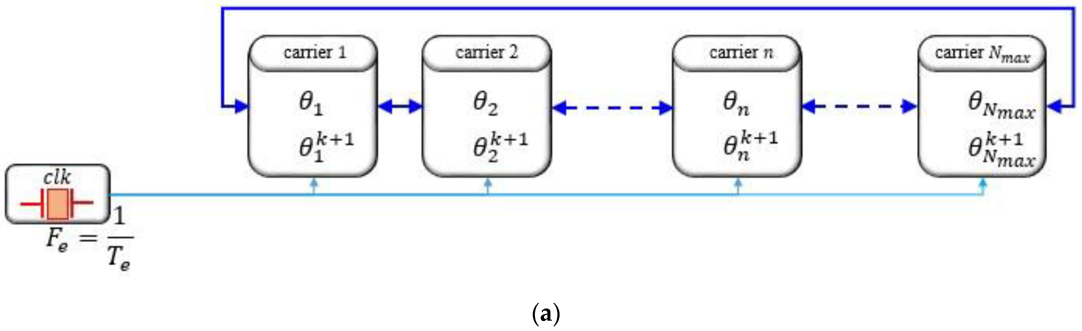
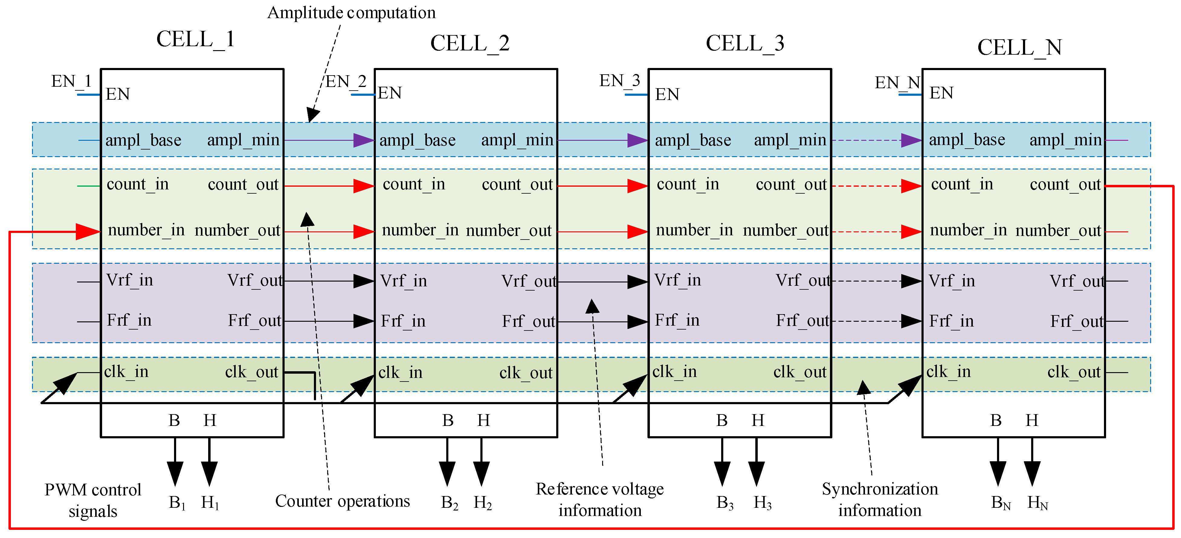
3. Proposed Decentralized Self-Aligned Carrier Method

In order to reduce the system configuration and reconfiguration time as well as to overcome some restrictions of conventional updating rules mentioned in Section 2, a digital method is proposed in this section for rapid and exact self-aligning carriers, and it can be applied to any number of carriers and to both phase-shifted and level-shifted carriers. Control algorithm, system topology, and evaluation of the proposed algorithm are discussed in detail, and simulation and experimental results are presented in the following sections.

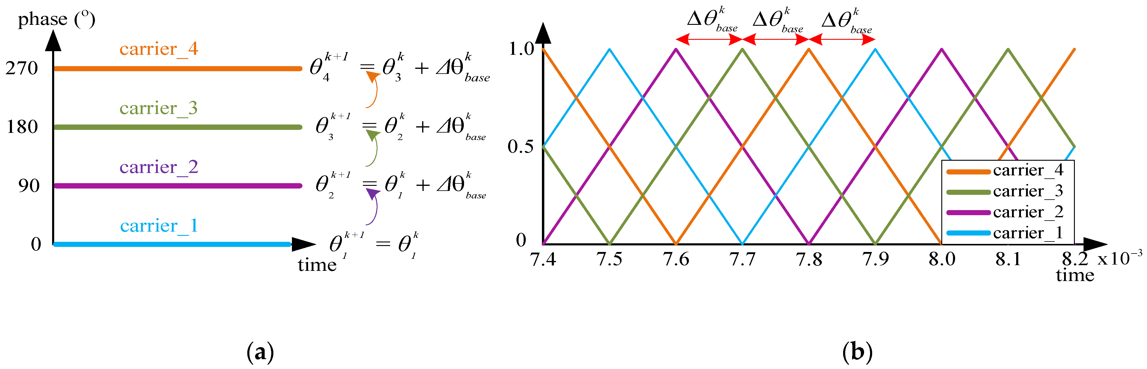
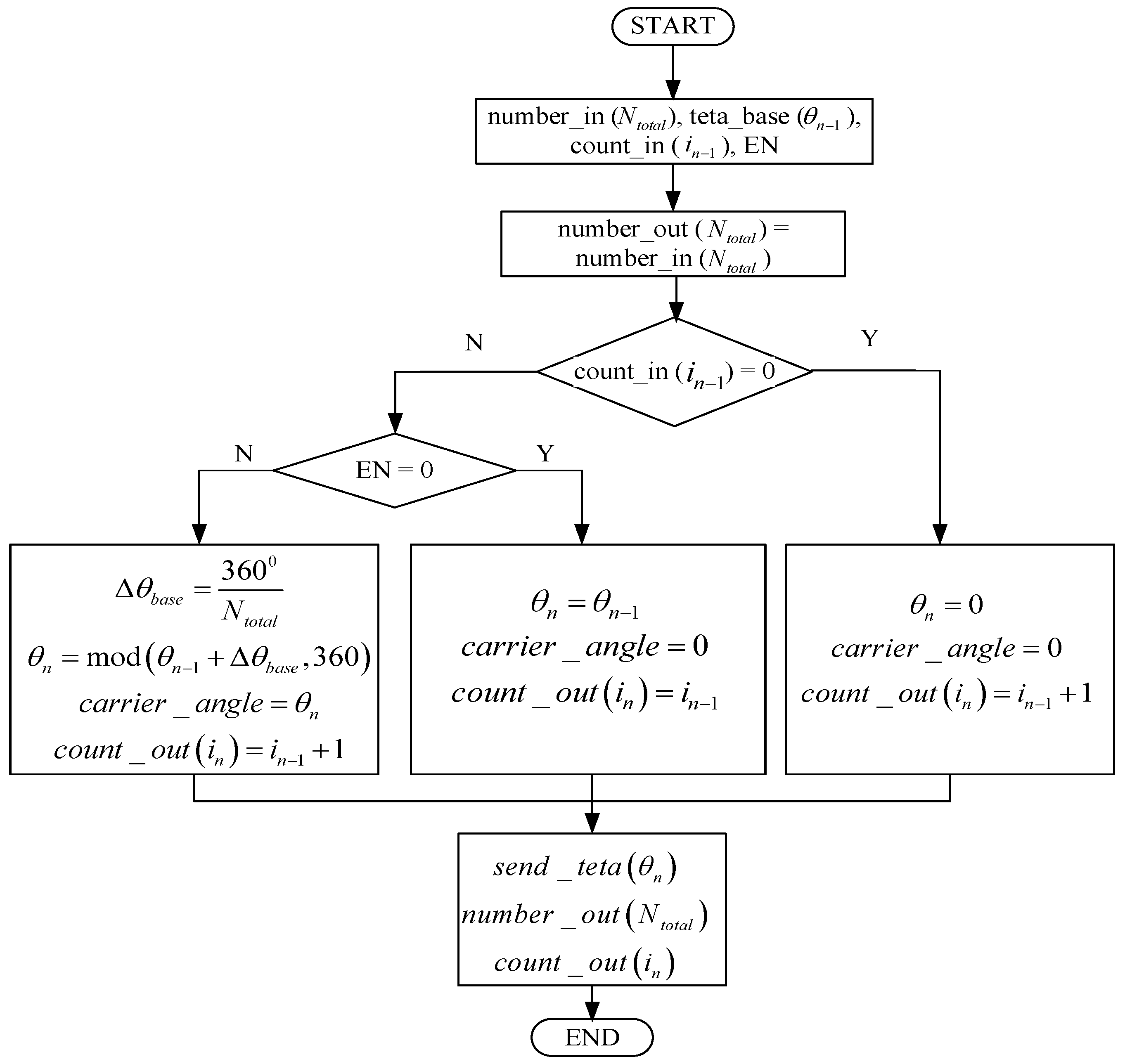
3.1. Proposed Decentralized Self-Aligned Phase-Shifted Carrier Method

This proposed method is named as decentralized self-aligned PS carriers (DSA-PSC), and its principle is shown graphically in Figure 4. In this method, the (n−1)th cell sends to the next nth cell the information of its angle (θn−1), its index number (in−1), and the total number of activated cells of the converter (Ntotal). Then, each cell controller determines the elementary phase-angle (Δθbase) and updates its own phase-angle (θn) based on the received information by using the Equations (4)–(7) as follows:
i n k + 1 = i n 1 k + 1 ; n [ 1 , 2 , N ]
{ N t o t a l _ 1 k + 1 = i N k N t o t a l _ n k + 1 = N t o t a l _ ( n 1 ) k ; n [ 2 , N ]
Δ θ b a s e k + 1 = 360 ° N t o t a l k
θ n k + 1 = m o d ( θ n 1 k + Δ θ b a s e k , 360 )
The indexing rule is simple; in cell n, at time step k, the index number i n 1 k of cell n−1 (named as count_in) is read and augmented by one and assigned as count_out ( i n k + 1 ), and this sequence is applied to all cells. Since the indexing communication line is an open loop chain, the cell at the open point has the index value i 1 k because the previous number read is zero (no information). The information count_out of last cell is recognized as the total number of activated cells in series, and it can be transmitted to all the cells via the numbering communication link (Figure 5).
Moreover, each cell transfers to its neighboring cell the information of referenced voltage (Vrf).
In Figure 5, the cell with index of zero is used as a master cell controller, which is, different from other cells, responsible for providing duty-cycle and clock synchronization for the rest of the system.
If a cell is indicated as a master cell controller, then the Vrf pin function is not used. The synchronous clock pulse frequency from the master cell controller is transmitted to all cells in the system.
The inputs and the outputs of a cell model are described in Table 1.
The flowchart algorithm of the proposed DSA-PSC method is shown in Figure 6. If a cell has to be removed from the converter, i.e., deactivated, the bypassing of a cell is realized using an enable bit (EN).

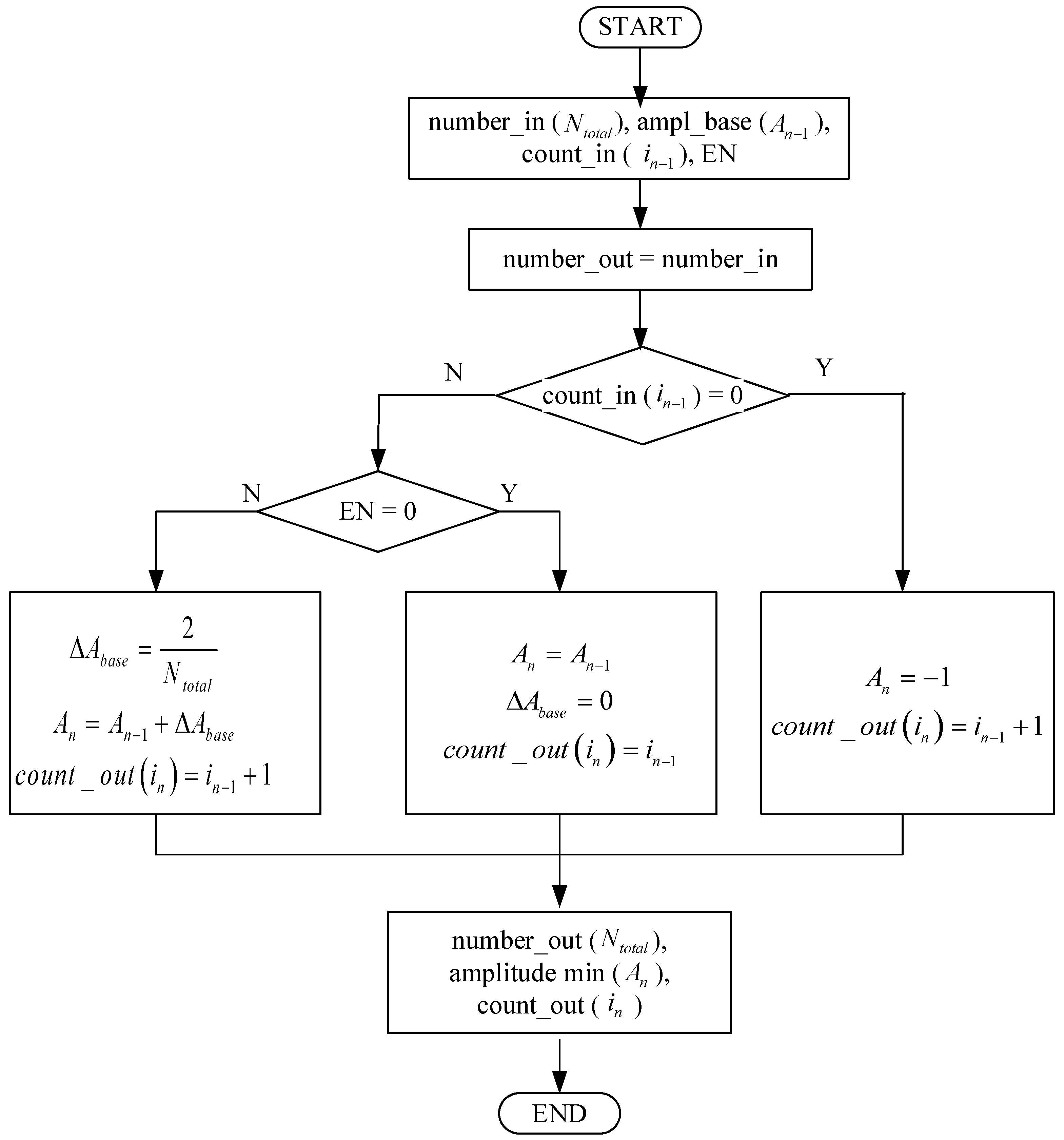
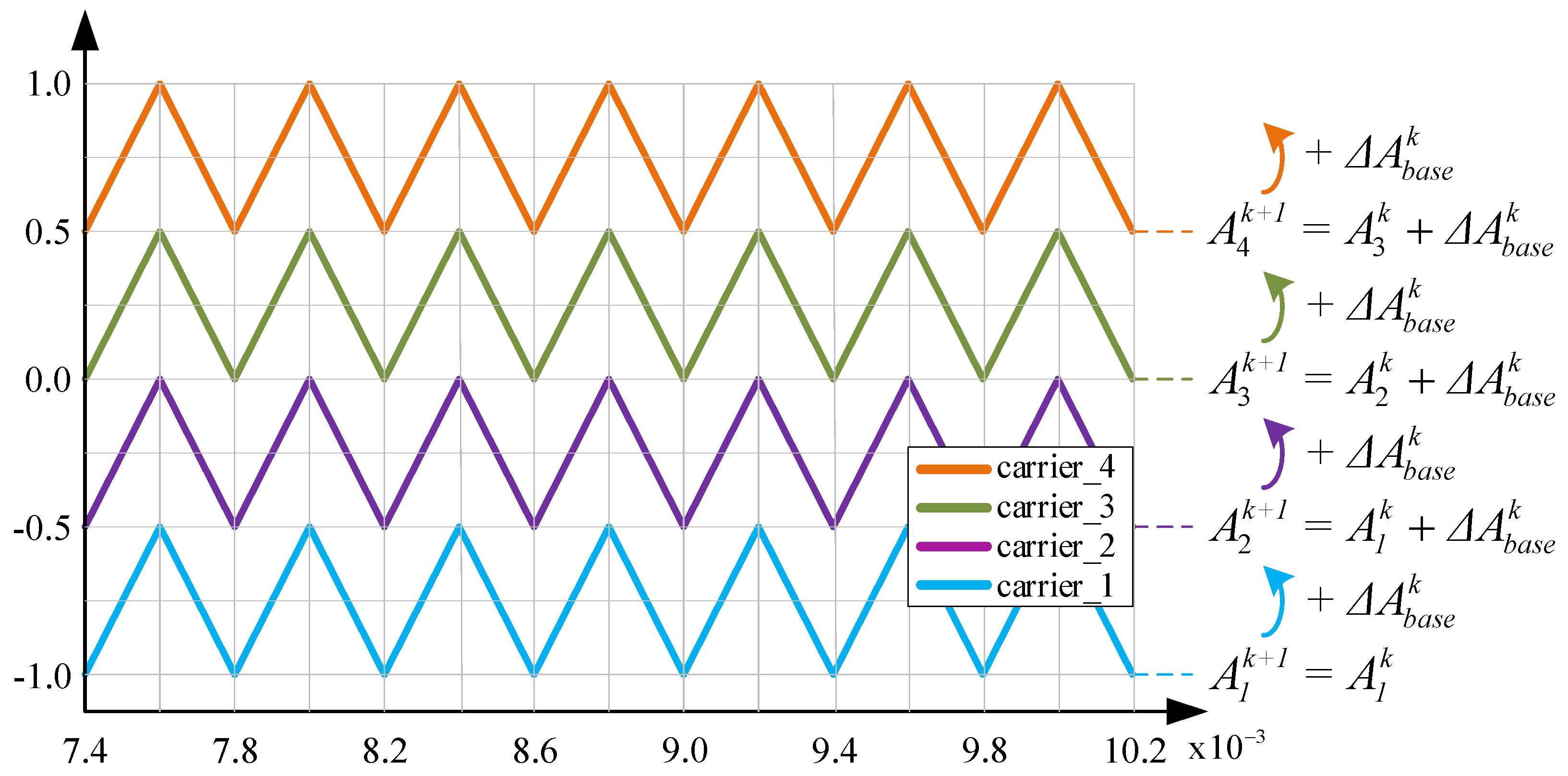
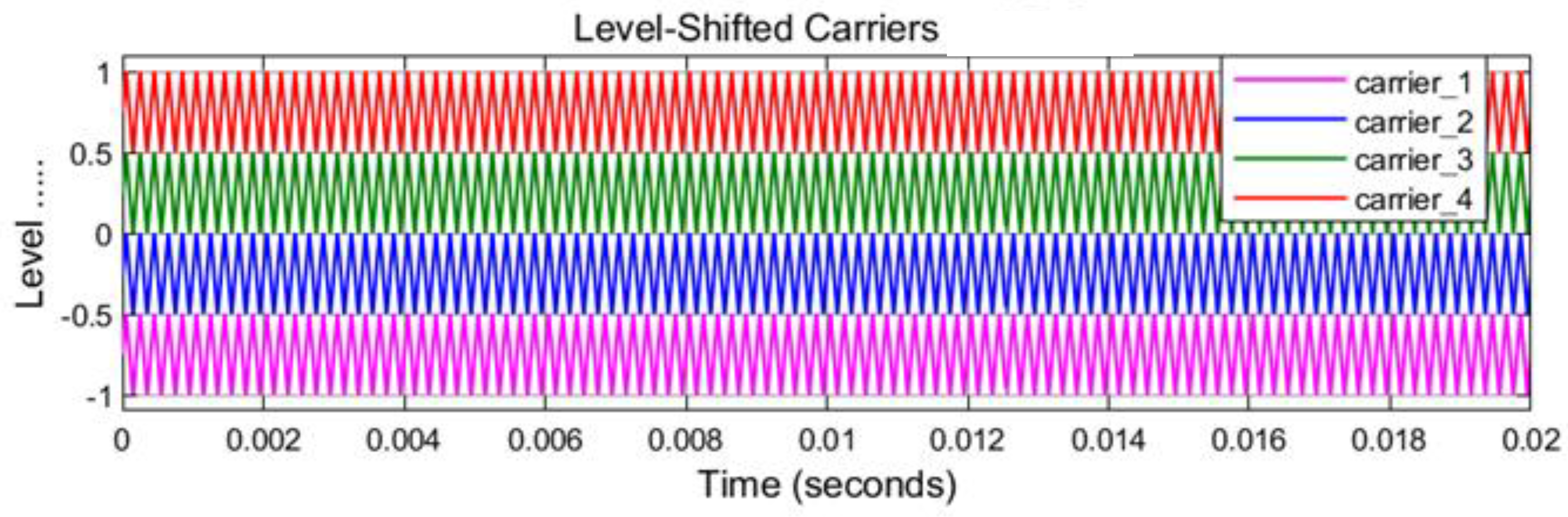
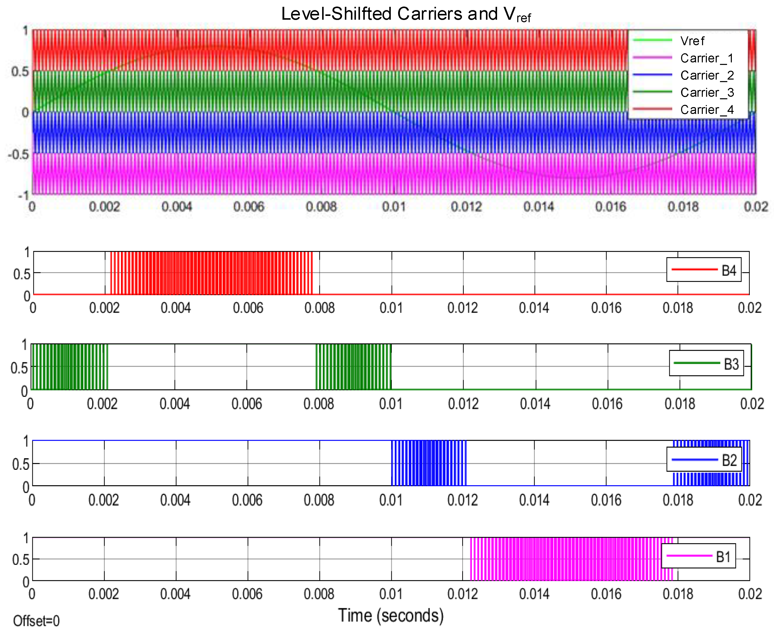
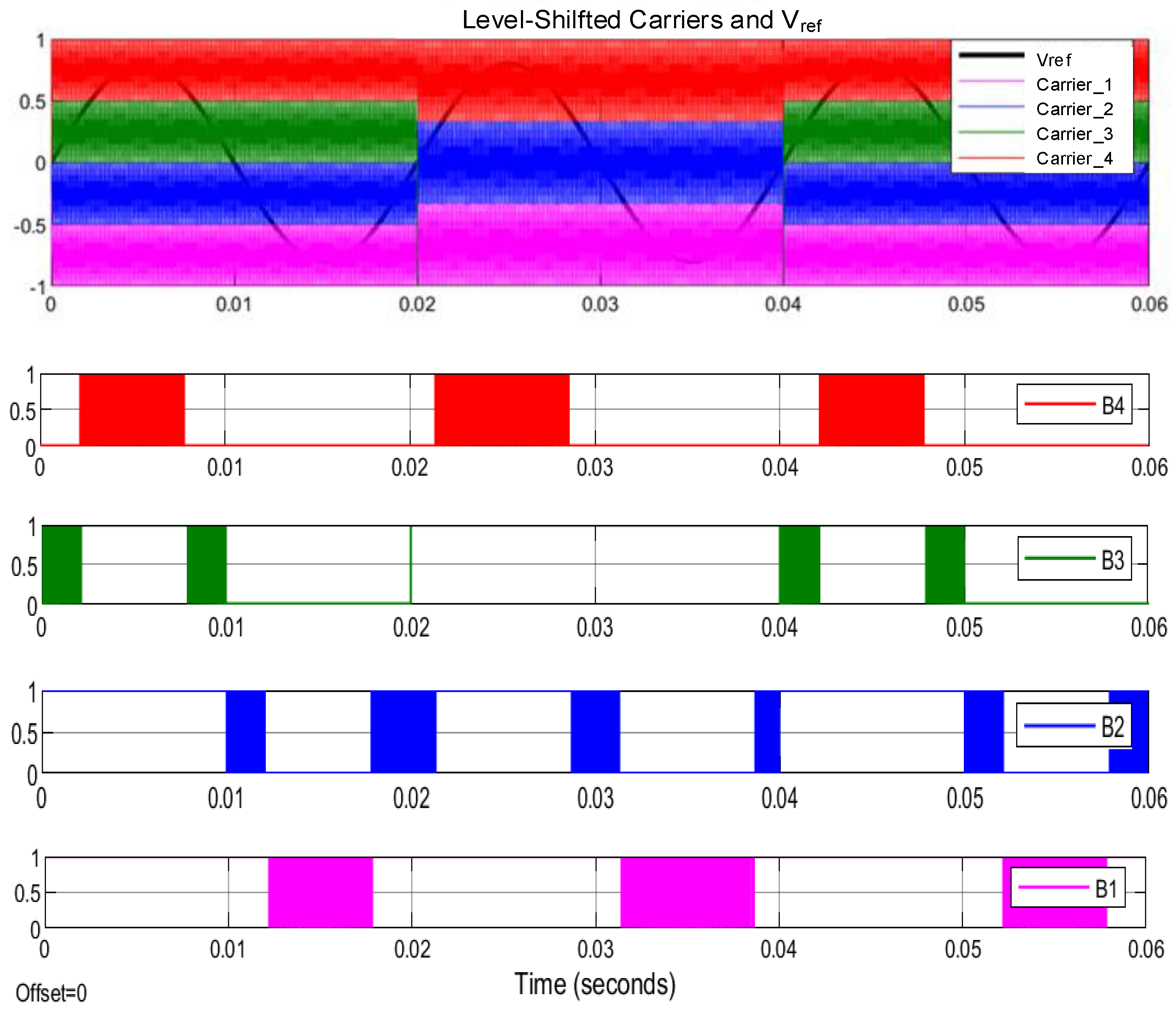
3.2. Proposed Decentralized Self-Aligned Level-Shifted Carrier Method

In many applications, multilevel converters are controlled by the level-shifted PWM method. With some modifications, the previous algorithm can also be applied to this converter type, and hereinafter, it is called a decentralized self-aligned level-shifted carriers (DSA-LSC) method.
In this method, the (n − 1)th cell sends to its next nth cell the information of its cell level (An−1,peak), its index number (in−1), and the total number of activated cells (Ntotal). Then, the nth cell controller updates its index number (in), the total number of cells (Ntotal) (see Equations (3) and (4)), and its carrier level by using the Formulas (8) and (9) as follows:
Δ A b a s e k + 1 = 2 N t o t a l k
A n k + 1 = A n 1 k + Δ A b a s e k
The indexing rule of cell n at time step k and the determination of total number of cells (Ntotal) shown in Figure 7 are treated similarly as in the DSA-PSC method. The inputs and the outputs of a cell controller in the DSA-LSC method are clarified in the Table 2. The flowchart algorithm of the proposed DSA-LSC method is presented in Figure 8. Figure 9 shows the rule to apply for the carrier level update with DSA-LSC method. Besides, each cell communicates with its neighboring cell and exchanges information of modulation index of referenced voltage (Vrf) and information of reference frequency (Frf).
Similar to the case in Figure 5, the cell with an index of zero in Figure 7 is used as a master cell controller, which is, different from other cells, responsible for providing the modulation index of reference voltage, reference frequency, and clock synchronization for the rest of the system.
If a cell is specified as a master cell controller, then Vrf and Frf pin functions are not used. The synchronous clock pulse frequency from the master cell controller is transferred to all cells in the system.

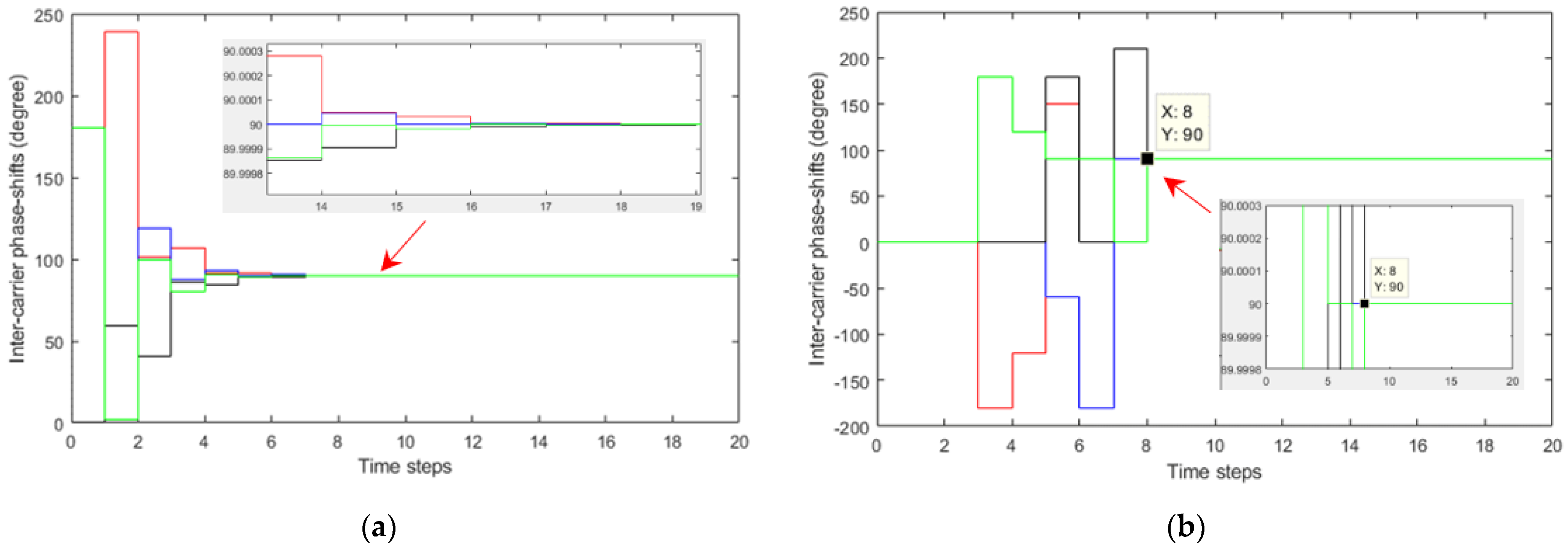
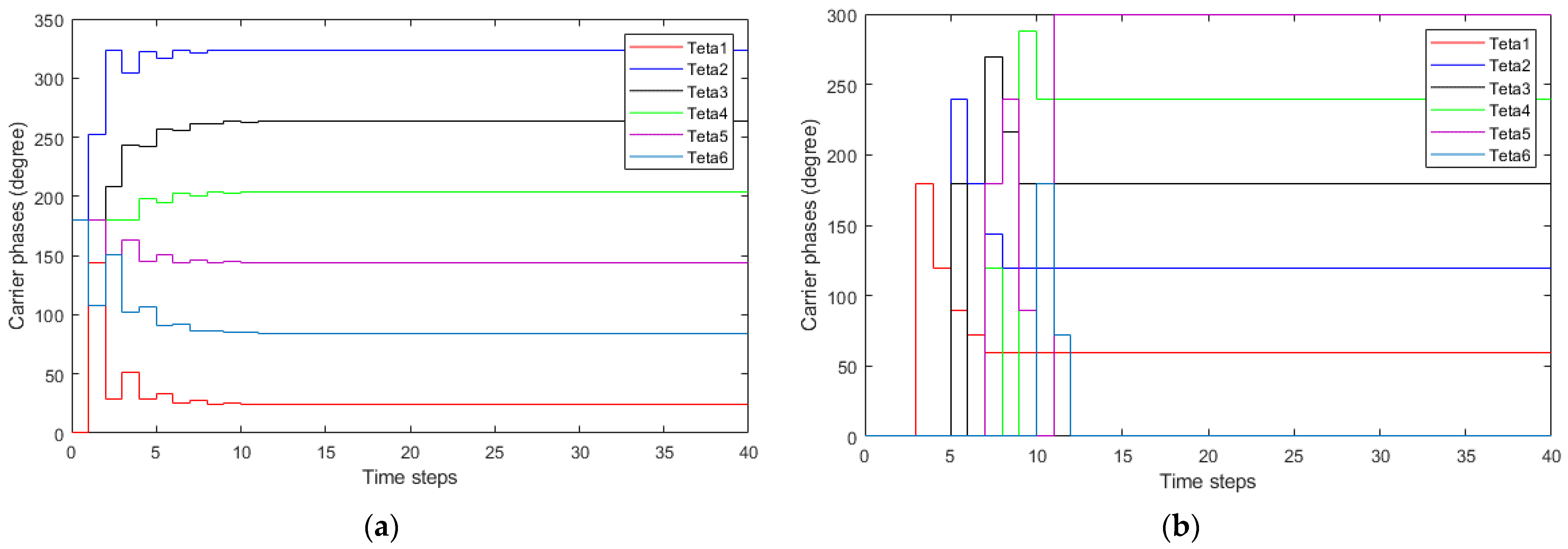
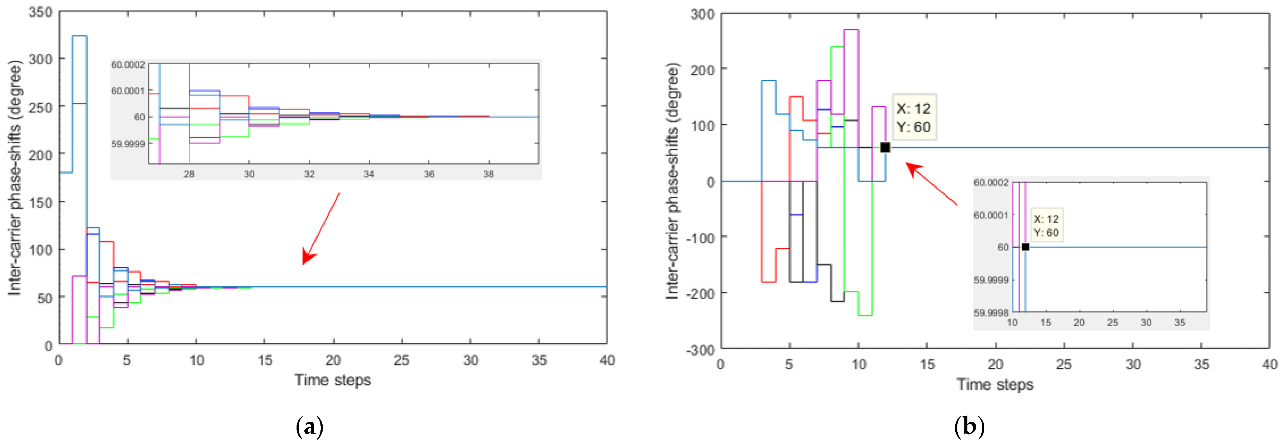
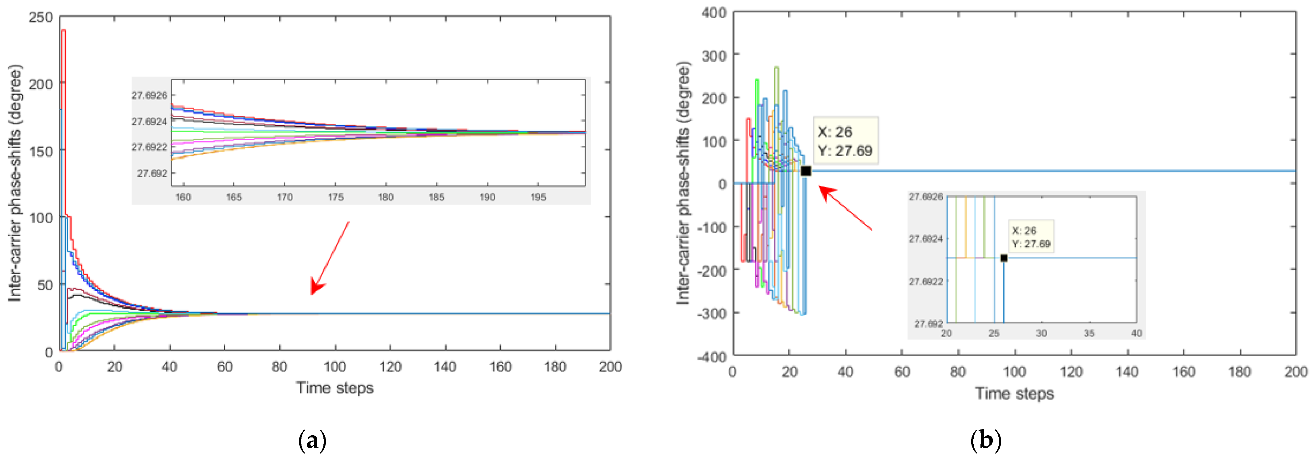
4. Simulation Results

4.1. Simulation Models

To verify the validity of the proposed algorithm, the models of the proposed DSA-PSC and DSA-LSC methods are built using MATLAB/Simulink software. Without loss of generality in number of phases or levels, Figure 10 demonstrates a four-phase DC/DC converter with DSA-PSC method, and Figure 11 presents a five-level inverter with DSA-LSC method. The parameters of these power converters are presented in Table 3 and Table 4.

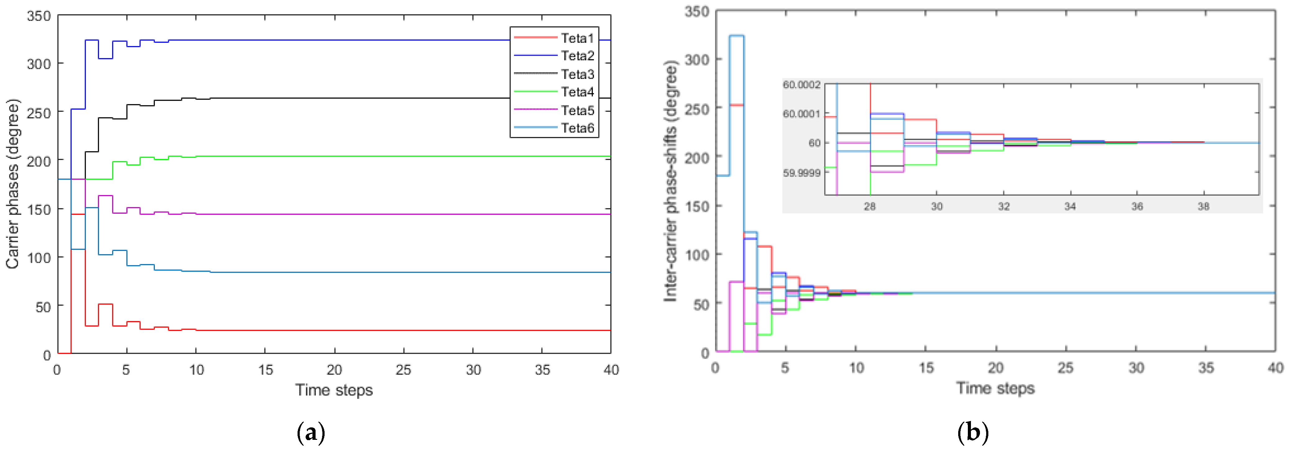
4.2. Evaluation of the Proposed DSA-PSC Method

Figure 12 shows the simulation results of the proposed DSA-PSC principle for the multiphase converter with four carriers (see Figure 10a). It can be seen that the self-alignment process of the carriers with the inter-carrier phase-shift Δθbase = 90° is perfectly realized, and the steady-state can be reached very quickly (after eight time steps). Figure 13 shows the PWM control signal generation for the high-side switches of each cell.
Figure 14 shows that the proposed control system works properly with fast transient responses on converter output voltages, load currents, and leg currents. In this figure, the system starts with four cells connected in series. At the time 0.4 s, cell 3 is removed, therefore, the current of leg 3 reduces to zero, and the converter output voltage fluctuates around 10% in about 1 ms before reaching steady-state. At time 0.7 s, cell 3 is restored, and leg 3 current quickly increases to the value 0.25Itotal after a transient time of 1 ms.
The advantage of the DSA-PSC method in terms of fast dynamic reconfigurations is also guaranteed when the number of cells is dynamically either deactivated or activated. To validate this point, Figure 15 shows the simulation of reconfigurations for a four-cell converter. At the beginning, the system starts with four interleaving cells involving four carriers with inter-carrier phase-shift Δθbase = 90°. Then, at time 0.5 ms (at time step 0.5 × 10⁴), the cell 3 is removed (using a internal by-pass function of the local controller), and the three remaining cells quickly adjust their own inter-carrier phase-shifts to reach Δθbase = 120°. Next, at time 1 ms (at time step 1 × 10⁴), the cell 2 is removed, and the system is still well interleaved by self adjusting the phase-shifts to Δθbase = 180°. Then, the cell 2 is reinserted at time 1.5 ms (at time step 1.5 × 10⁴), resulting in a new inter-carrier phase-shift Δθbase = 120°. Finally, the cell 3 is re-activated at time 2 ms (at time step 2 × 10⁴), and the system returns quickly to the original configuration with a correct interleaving of the carriers.

4.3. Evaluation of the Proposed DSA-LSC Method

Figure 16 shows the simulation results of the proposed DSA-LSC principle for a five-level inverter which is controlled by four level-shifted carriers (see Figure 11a). The system carriers reach their final levels at steady-state quickly (i.e., without iterations) and correctly. The PWM signals at the gate of the high-side switches of the converter cells (B1B4) are shown in Figure 17. The output voltage and the output current waveforms are presented in Figure 18. It can be seen that the control system works properly with fast transient response.
To validate the reconfiguration capability of the system in the case of removing or inserting a cell, Figure 19 demonstrates the process of reconfigurations for this four-carrier system. At the beginning, the system has four active cells with four perfect level-shifted carriers generated using the DSA-LSC method, as observed from time 0 to 0.02 s. Then, at time 0.02 s, the cell 3 is removed, and the system is reconfigured instantly with three level-shifted carriers. Finally, this cell is re-activated at time 0.04 s, and the system returns quickly to the original configuration with four properly level-shifted carriers.
The output voltage waveform of the investigated inverter during reconfiguration process is shown in Figure 20.

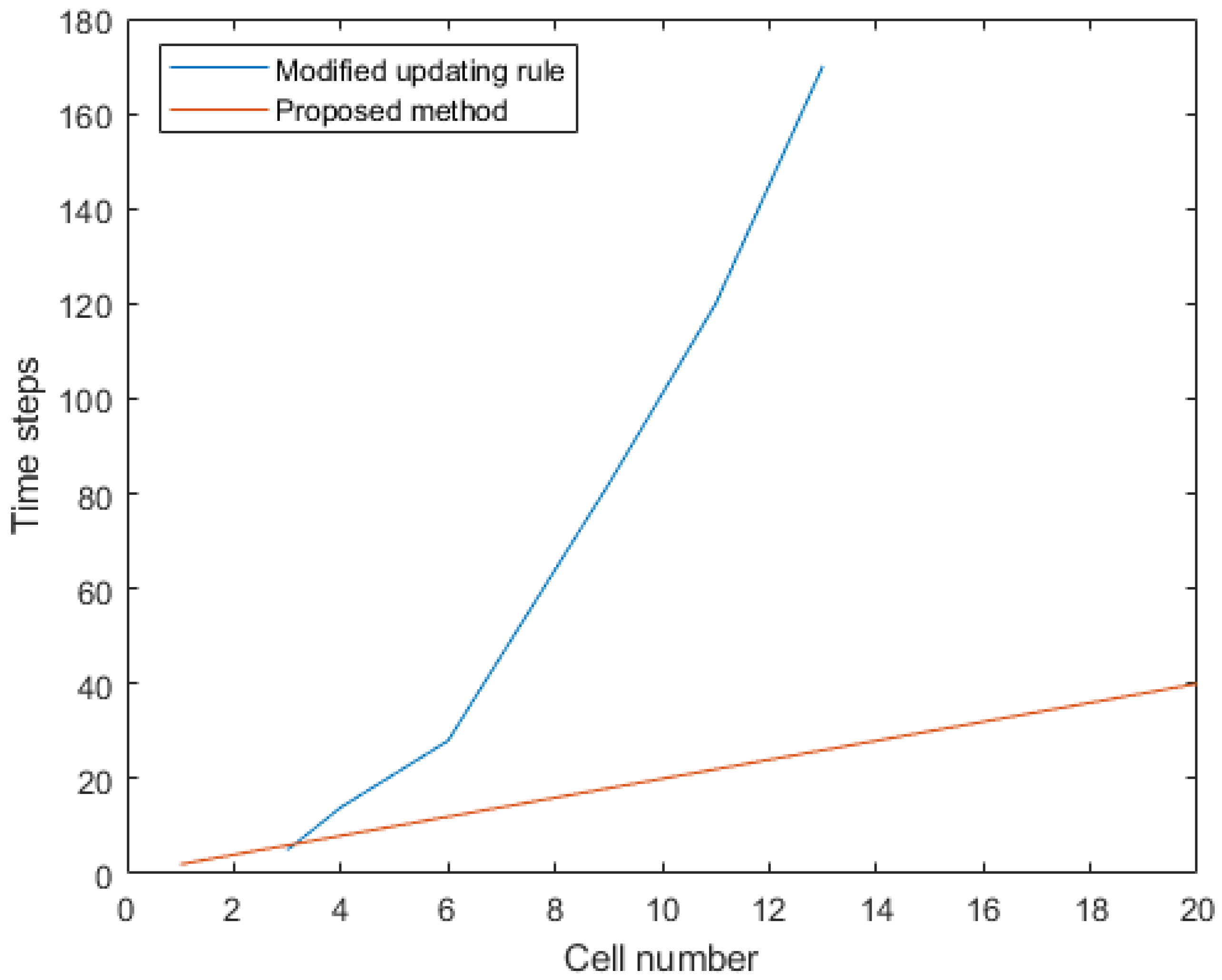
4.4. Evaluate the System Configuration Time

From the cell controller connection of DSA-PSC method and DSA-LSC method, shown accordingly in Figure 5 and Figure 7, it can be seen that, from starting up, both methods reach the steady-state after 2N time steps. Therefore, the configuration time of both methods is:
T c o n f i g u r a t i o n = 2 N T s
where N is the number of active cells and Ts is the sampling time.
Figure 21 compares the configuration time of the conventional method (using modified updating rules in (2) with K = 0.66) to that of the proposed self-aligned phase-shifted carrier method. For estimating its configuration time, the conventional method is simulated with different values of N, and the system is considered as reaching steady-state when the errors of inter-carrier phase-shifts are smaller than 10−4 degree (i.e., ε(Δθn, n+1) ≤ 10−4 degree). Meanwhile, the configuration time of the proposed DSA-PSC method is estimated directly using (10). From Figure 21, it can be seen that the reduction of configuration time is the key advantage of the proposed DSA-PSC method. The higher the number of cells is, the larger the reduction of time steps of the proposed method to reach the steady-state is.
To study in detail the configuration process of the conventional method and the proposed method, simulations are conducted for the systems controlled by these methods with different values of cell numbers (N = 4, 6, and 13). For each value of N, the variation of carrier phases as well as inter-carrier phase-shifts during starting up processes of both control methods are presented in Figure 22 and Figure 23 (for N = 4), in Figure 24 and Figure 25 (for N = 6), and in Figure 26 and Figure 27 (for N = 13). These simulation results confirm the advantage of the proposed DSA-PSC method in terms of lower configuration time and zero inter-carrier phase-shifts relative error, which is summarized in Table 5.
Moreover, it should be noted that the proposed method can be applied to any number of carriers (N ≥ 1), and it is different from the conventional method, which can be applied only for the system with N ≥ 3, as mentioned in Section 2.

4.5. Evaluate the System Reconfiguration Time

To evaluate the system reconfiguration time of the proposed DSA-PSC method, Figure 28 shows the simulation of reconfigurations for a six-cell converter using the CPSC method (with modified updating rule) as well as the proposed DSA-PSC one. At the beginning, the system starts with six interleaving cells involving six carriers with inter-carrier phase-shift Δθbase = 60°. Then, at time 0.5 ms (at time step 0.5 × 10⁴), the cell 3 is removed, and the five remaining cells adjust their own inter-carrier phase-shifts to reach Δθbase = 72°. Next, at time 1 ms (at time step 1 × 10⁴), the cell 5 is removed, and the system is interleaved by self adjusting the phase-shifts to Δθbase = 90°. Then, the cell 5 is reinserted at time 1.5 ms (at time step 1.5 × 10⁴), resulting in a new inter-carrier phase-shift Δθbase = 72°. Finally, the cell 3 is re-activated at time 2 ms (at time step 2 × 10⁴), and the system returns to the original configuration.
The reconfiguration time study of two methods shown in Figure 28 approves the advantage of the proposed DSA-PSC method in terms of lower reconfiguration time with zero inter-carrier phase-shifts relative error, which is summarized in Table 6.

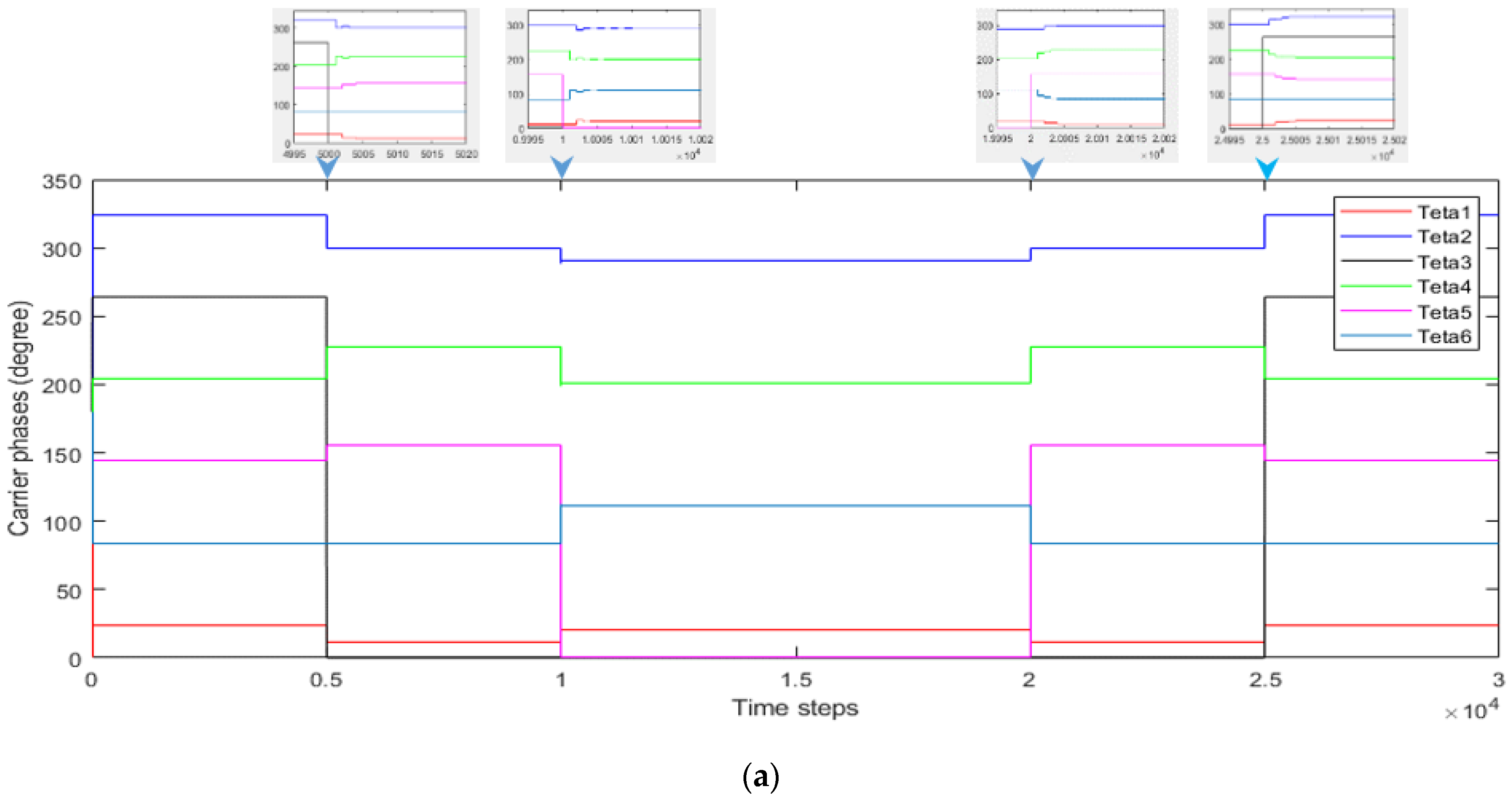
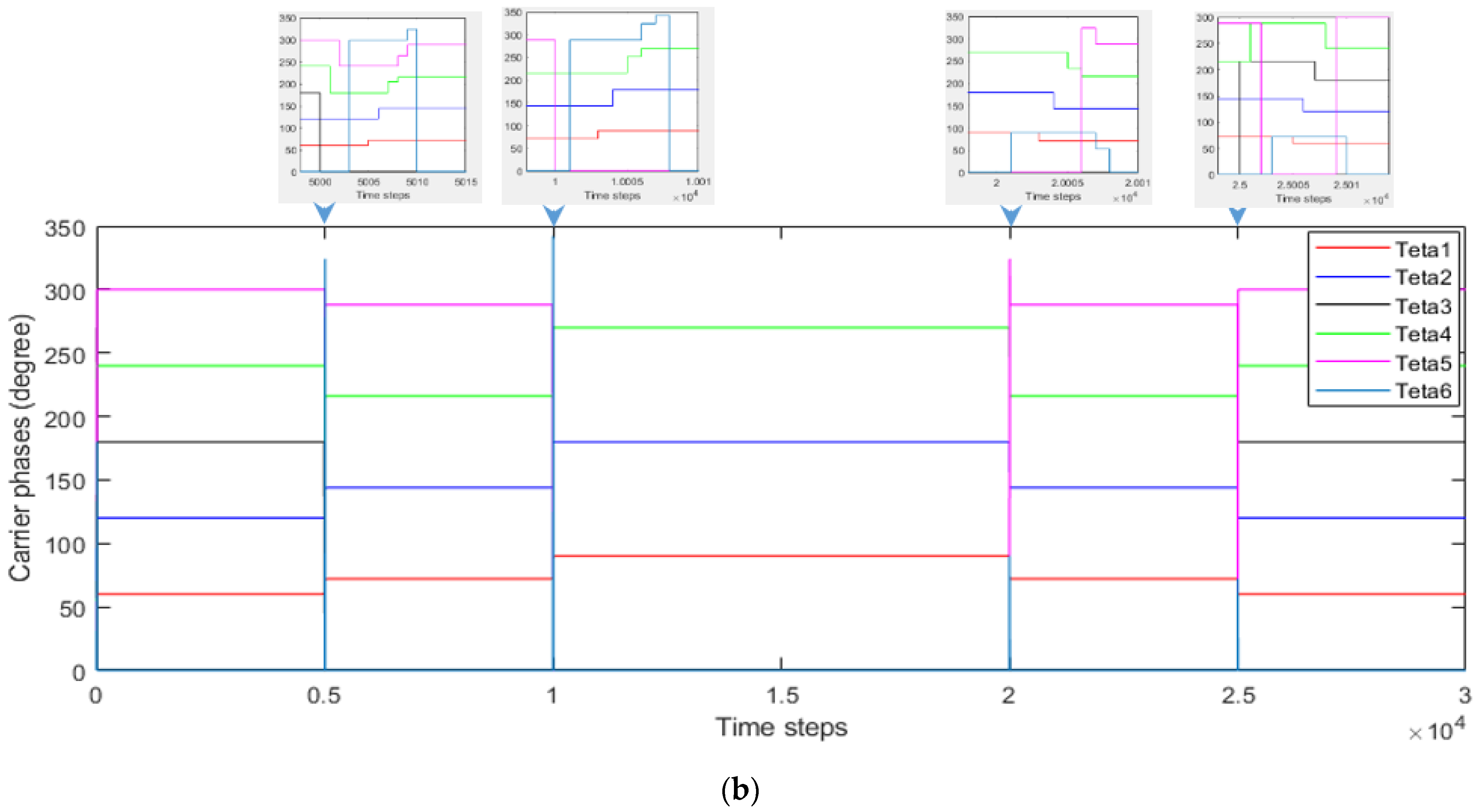
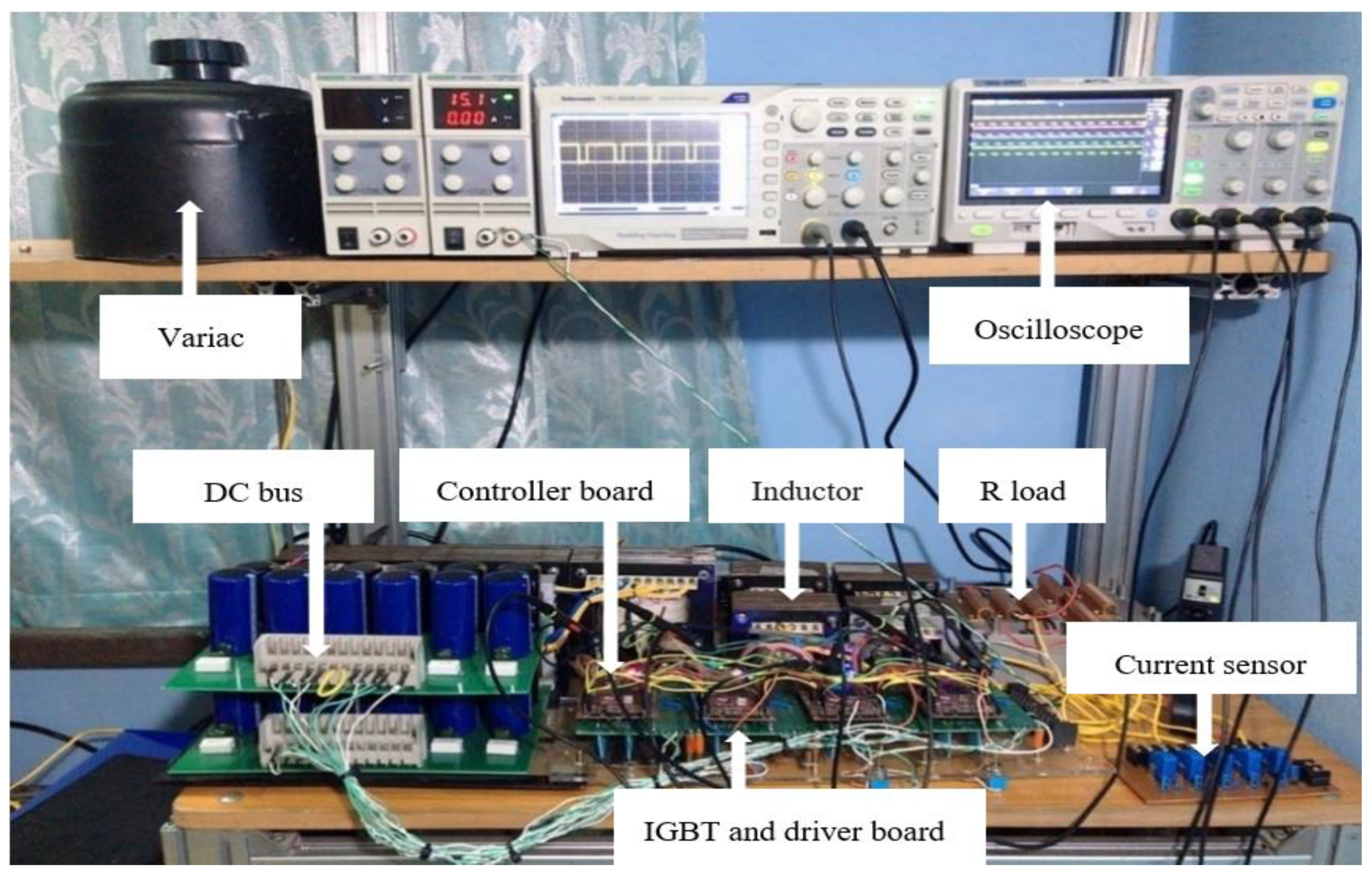
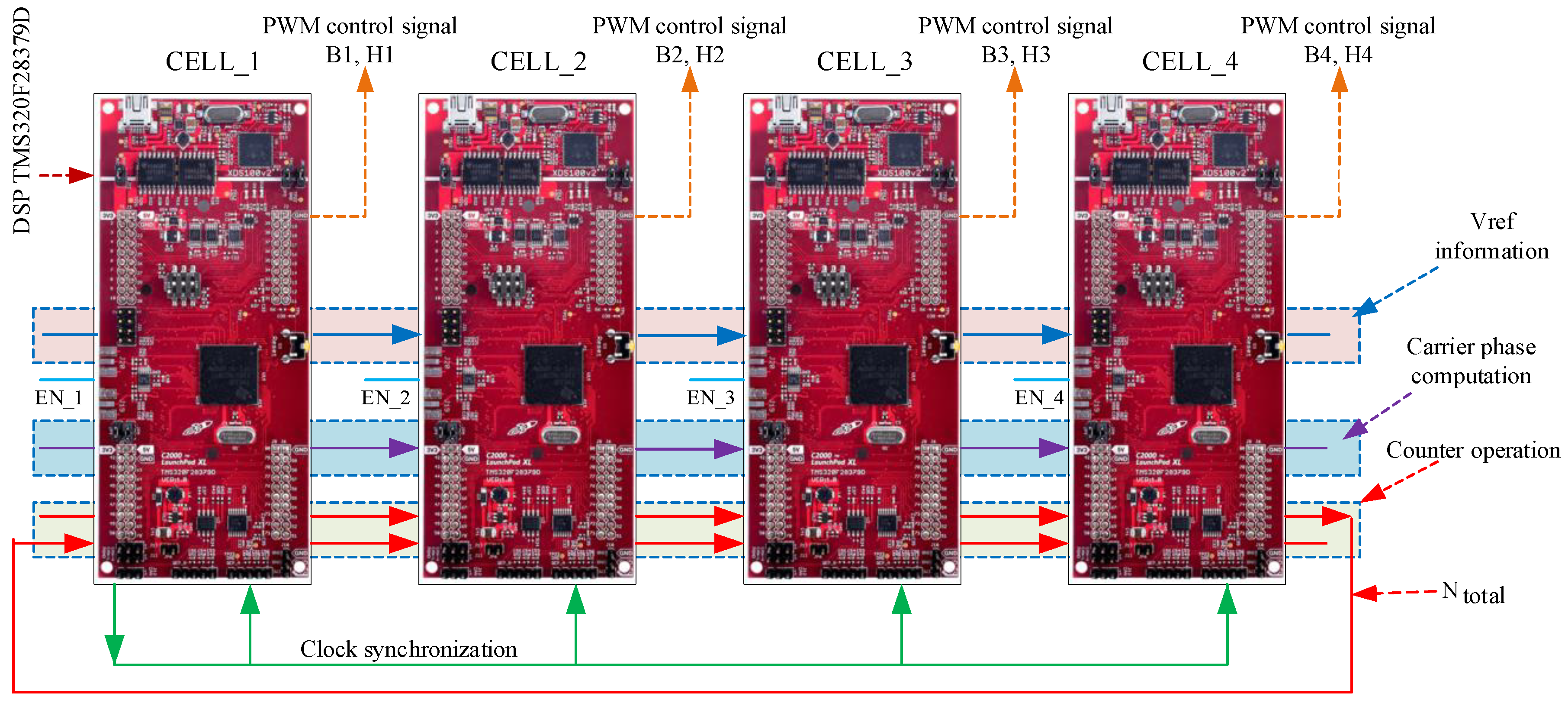
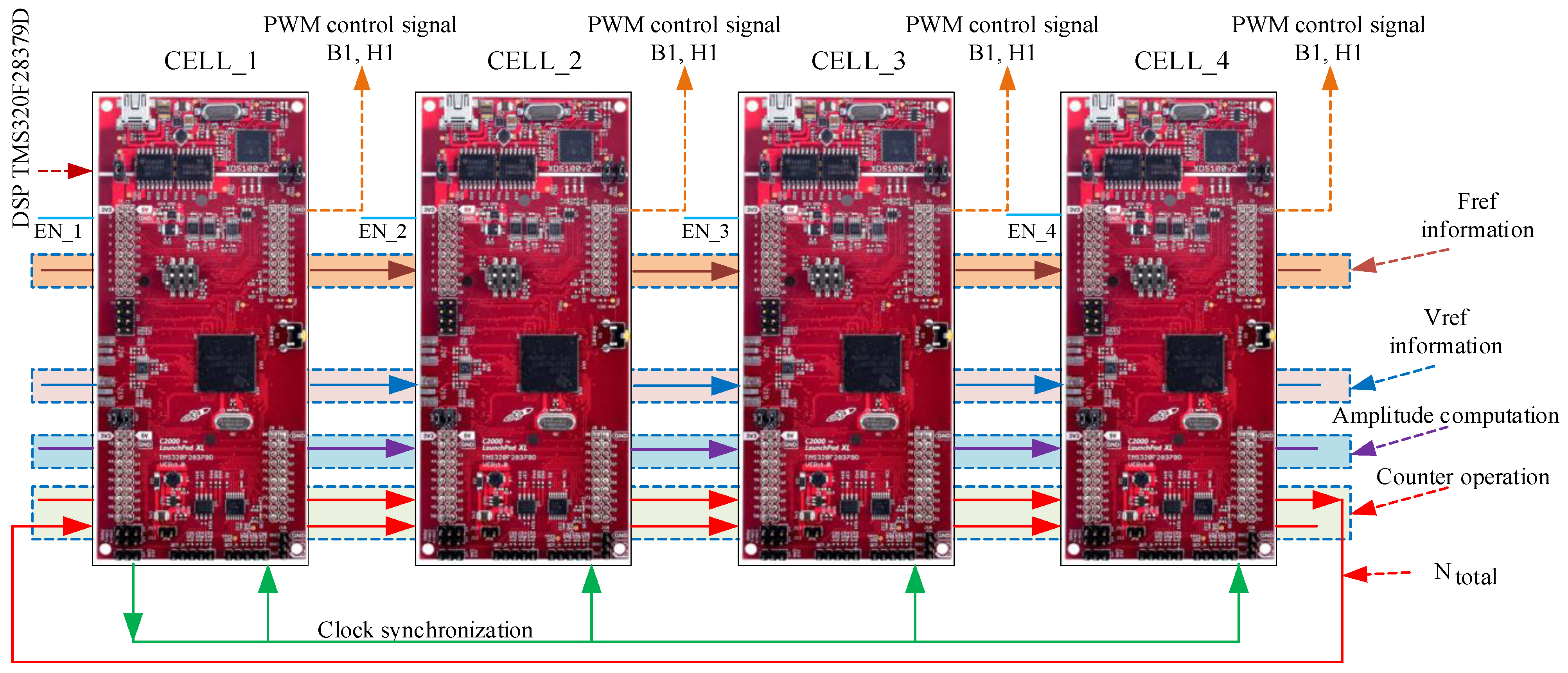
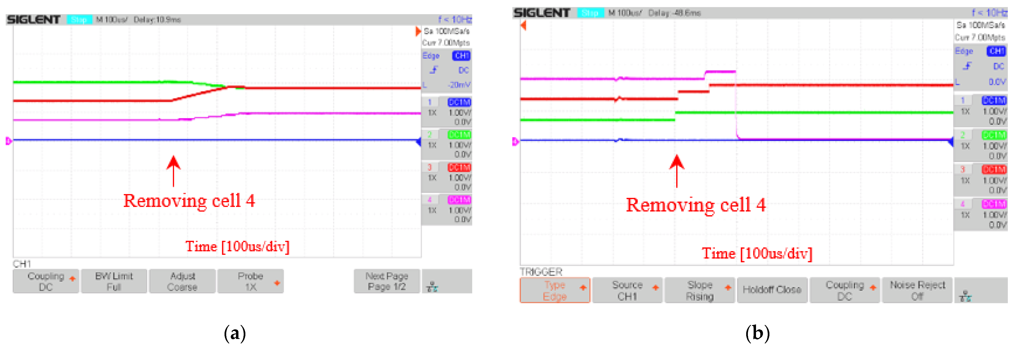
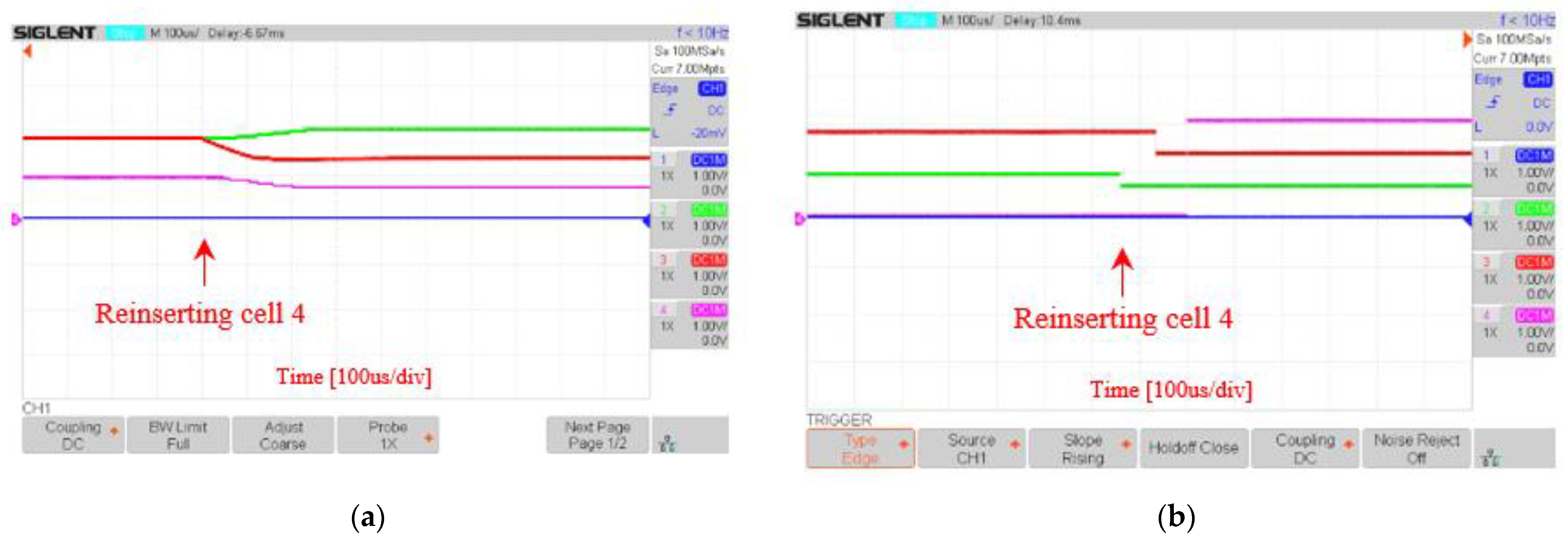
5. Experimental Result

Figure 29 shows the experimental setup of the four-cell converter system with the load to verify the proposed control algorithm. Each converter cell consists of a DSP controller, a driver circuit, and an IGBT power module. The topology of the power converter is presented in Figure 10a and Figure 11a. Information on experimental components is given in Table 7. The DSP controller is the LaunchPad Development Kit using C2000 Delfino MCUs F28379D from Texas Instrument (TI). With this setup, the experimental results of the conventional method and the proposed method can be obtained by changing only the DSP program accordingly whilst keeping the system hardware unchanged.
Further, for rapid programming, the DSP is coded using the Matlab/Simulink software combining with the Code Composer Studio (CCS) compiler from TI, which is proposed in the previous works [32,33,34]. The programming sequence is conducted in three steps: (1) the model of the control algorithm is built using Matlab/Simulink; (2) the Real-Time Workshop® in Matlab generates C code file from this model; (3) the C code file is downloaded into the DSP board using the CCS compiler.

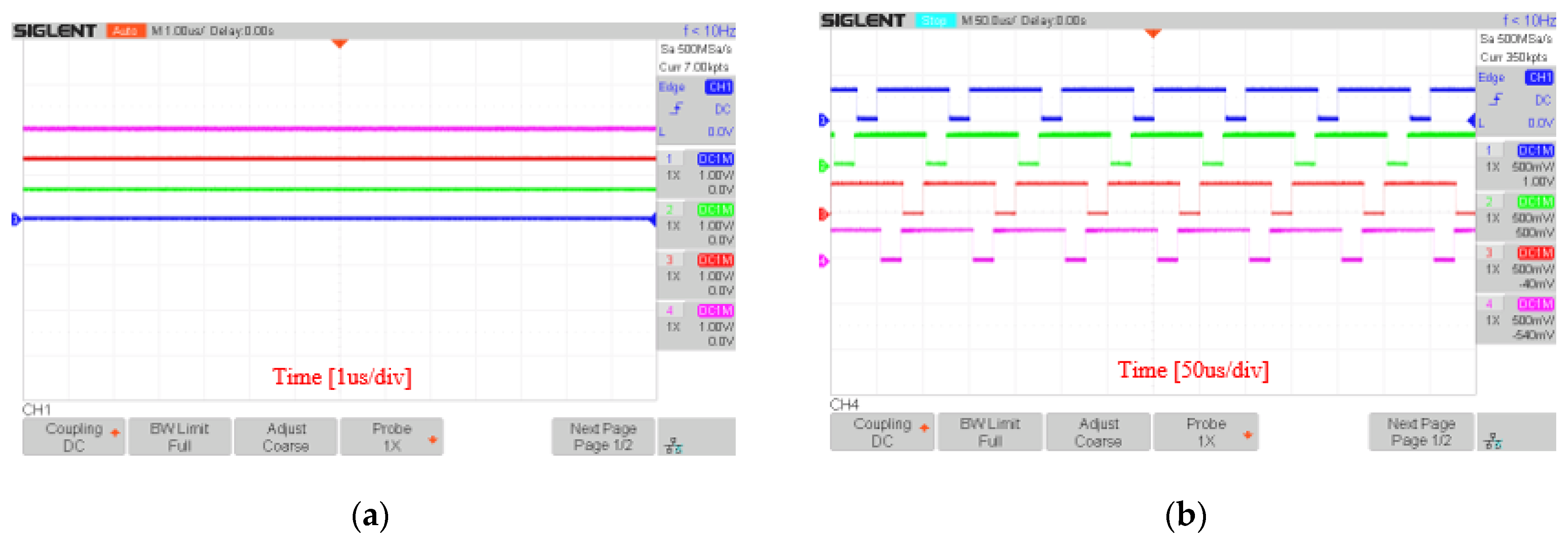
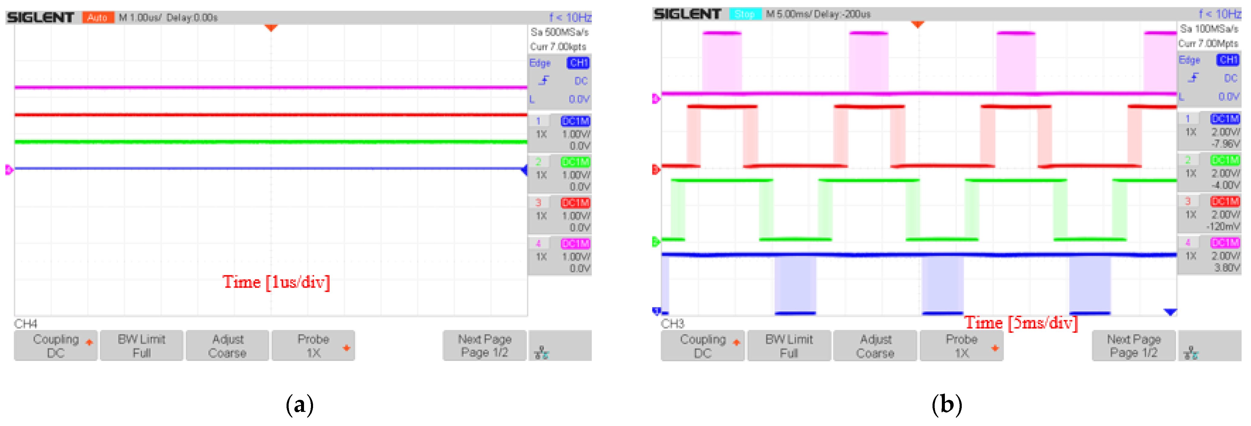
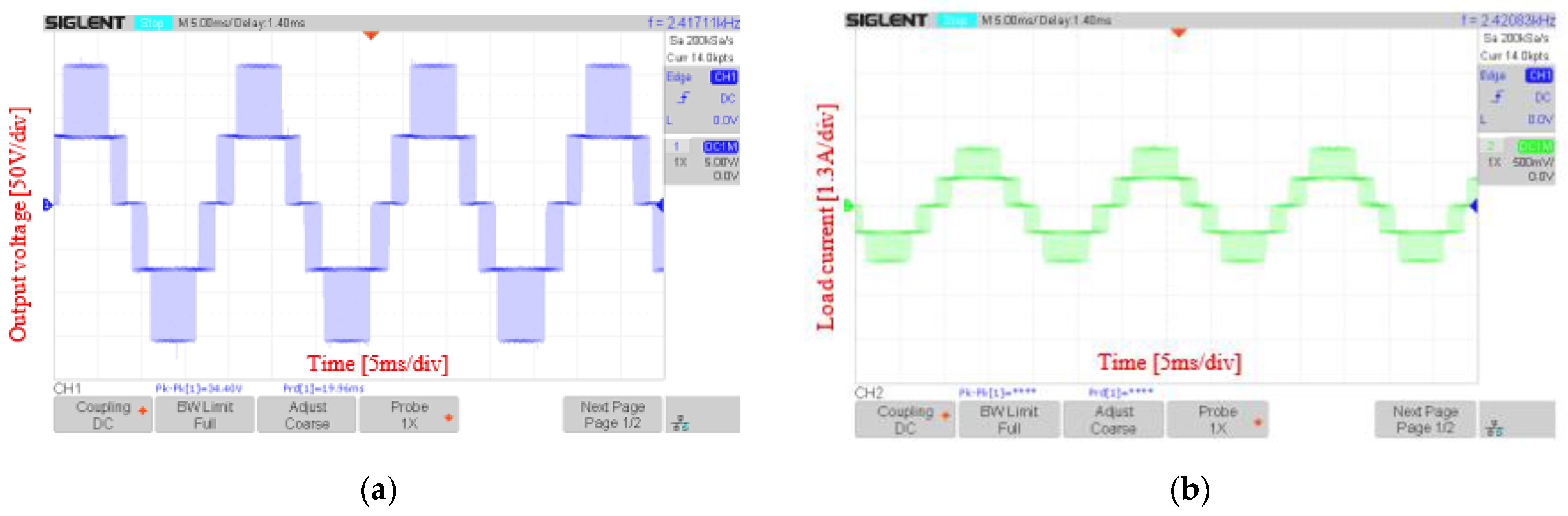
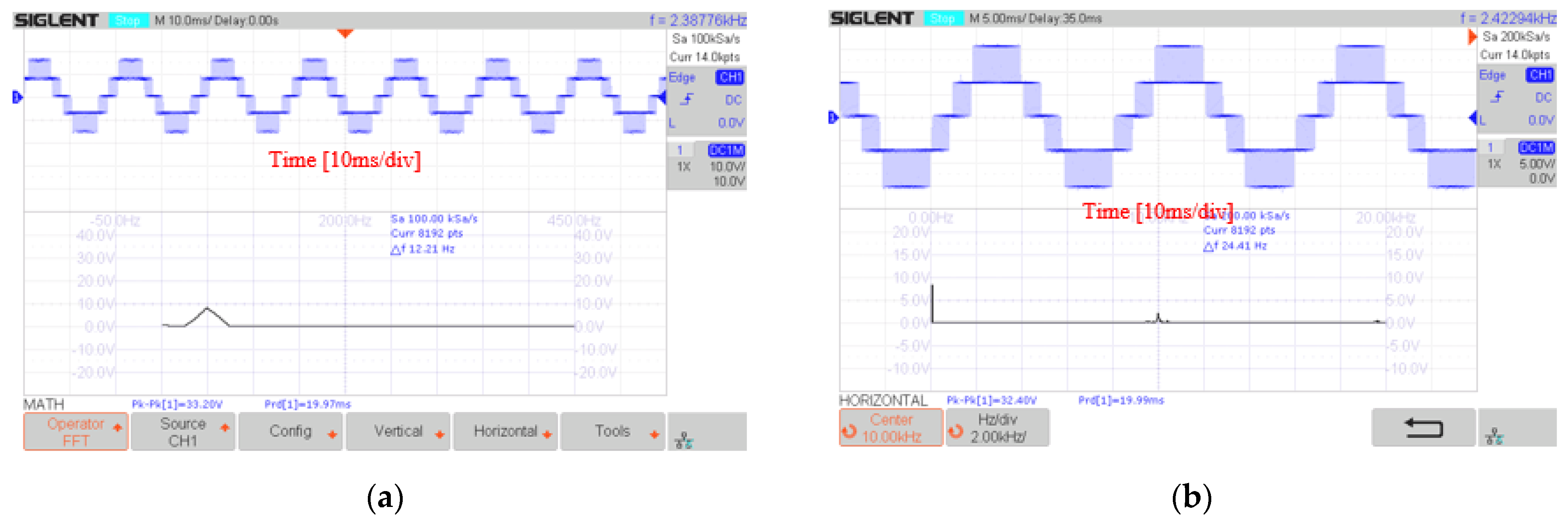
5.1. Experiment with DSA-PSC Method

Figure 30 shows the connection diagrams for DSA-PSC method, each cell is controlled by a DSP controller and communicates with other cells via the functional pins described in Table 8. Parameters of four-phase converter (Figure 10a) with algorithm DSA-PSC are shown in Table 9.
Figure 31 depicts the arrangement of the carrier phases and the IGBT control signals when all cells are active. Figure 31a shows that four triangular carriers are arranged with an exact 90° phase-shift, resulting in four PWM control signals (to the four high-side cell switches) with same duty-cycle and same inter-carrier phase-shift, as shown in Figure 31b. When cell 3 is deactivated, the system has three remaining cells, and their carriers are rearranged at an exact 120° phase-shift, as shown in Figure 32a, and the triggering pulses are also rearranged to three pulses with 120° inter-carrier phase-shift, as shown in Figure 32b. When both cells 3 and 4 are deactivated, the system has two remaining cells, and their carriers are rearranged 180° apart, as shown in Figure 33a, and the triggering pulses are also changed accordingly to two pulses with 180° inter-carrier phase-shift (Figure 33b).
The transient system response of phase-shift arrangement in the case of deactivating cell 3 is illustrated in Figure 34a. It can be seen that it takes around 200 μs (at 10 kHz) to complete the reconfiguration of system carriers. After that, the three remaining triggering pulses are rearranged with the same inter-carrier phase-shift among pulses, as shown in Figure 34b.
Figure 35a shows the transient system response of reconfiguring a system from three cells to four cells (reactivating cell 4 while the other three cells are running). This system response takes around 150 μs to complete, and then the system has four PWM control signals with appropriate inter-carrier phase-shift balance.
Figure 36 and Figure 37 show the output voltage and the current waveforms when removing and reinserting cell 3, respectively. These results show that the voltage presents a very low ripple. When the system is reconfigured (i.e., adding or removing a cell), the voltage fluctuation during the transient is about 1%, and the output voltage reaches steady-state within a very short transient time (as shown in Figure 36 and Figure 37).

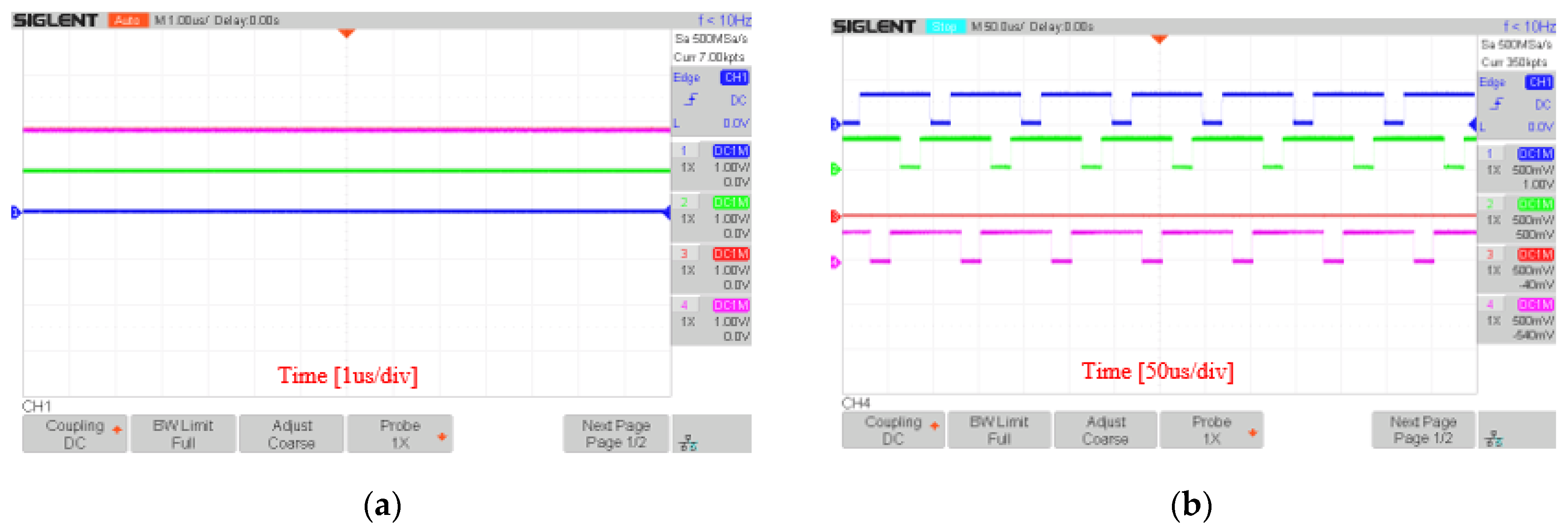
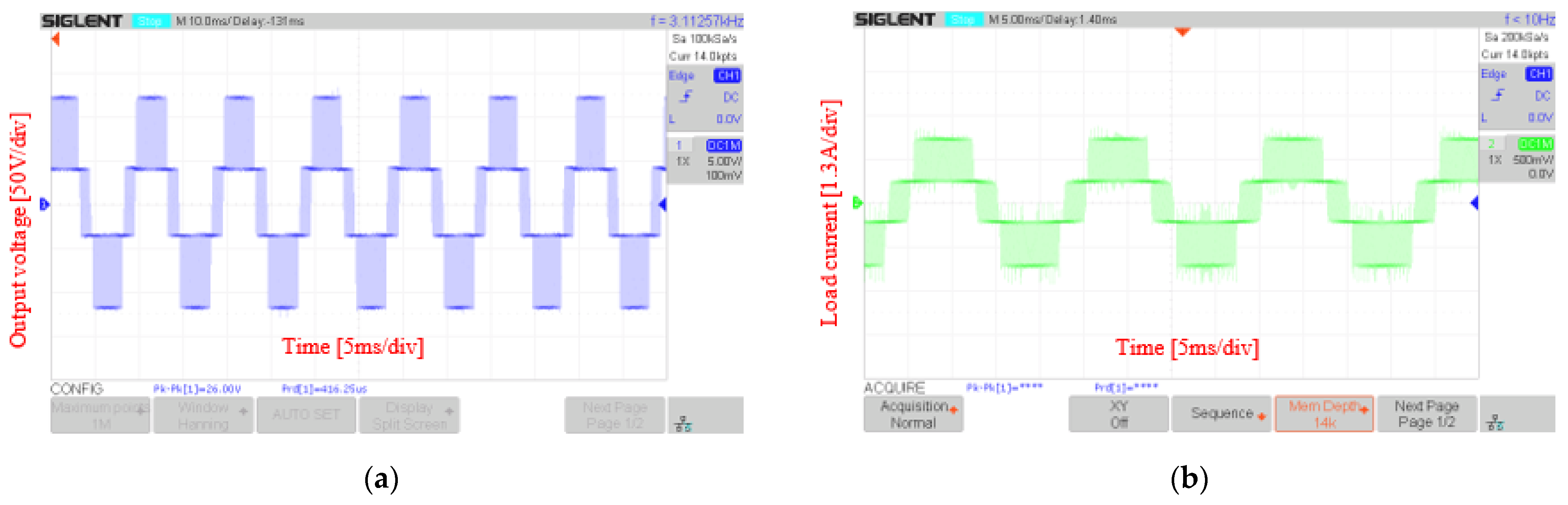
5.2. Experiment with DSA-LSC Method

Figure 38 shows the connection diagrams for DSA-LSC method; each cell is controlled by a DSP controller and communicates with other cell via the pins described in Table 10. Parameters of five-level converter (Figure 11a) with the algorithm DSA-PSC are presented in Table 11.
Figure 39a describes the arrangement of carrier levels (An) when the system has four cells, and Figure 39b shows the triggering pulses sent to the IGBTs of cells, which are correctly interleaved, and accordingly to a four-cell five-level converter.
Figure 40, Figure 41 and Figure 42 show the system response of a reconfiguration event, the output voltage levels, and the cell IGBT PWM control signals when adding or removing one or more cells. Figure 40 shows the system response when the system is reconfigured from four cells to three cells (by removing cell 3). Figure 41 shows the system response when cell 3 is added into an operating three-cell system. Figure 42 shows the system response when cell 4 is removed and added into an operating three-cell system. In these figures, the reconfiguration system response takes about 300 µs to complete.
Figure 43 shows the output voltage and the load current of the converter when all four cells of the converter operate. In this case, the output voltage has five levels, as shown in Figure 43a. Figure 44 shows the output voltage and the load current waveforms when one cell is removed and the system has 3 cells left, resulting in four-level output voltage, as shown in Figure 44a.
Figure 45 shows the transients of output voltage and load current when cell 3 is removed and reinserted; in this case, the DSA-LSC method is applied for each cell controller.
Figure 46 shows the FFT analysis of the output voltage, where Figure 46a shows the voltage FFT spectrum within the frequency range from 0 to 450 Hz, and Figure 46b shows the voltage FFT spectrum within the range from 0 to 20 kHz. The FFT analysis results show that the output voltage has low harmonic distortion.

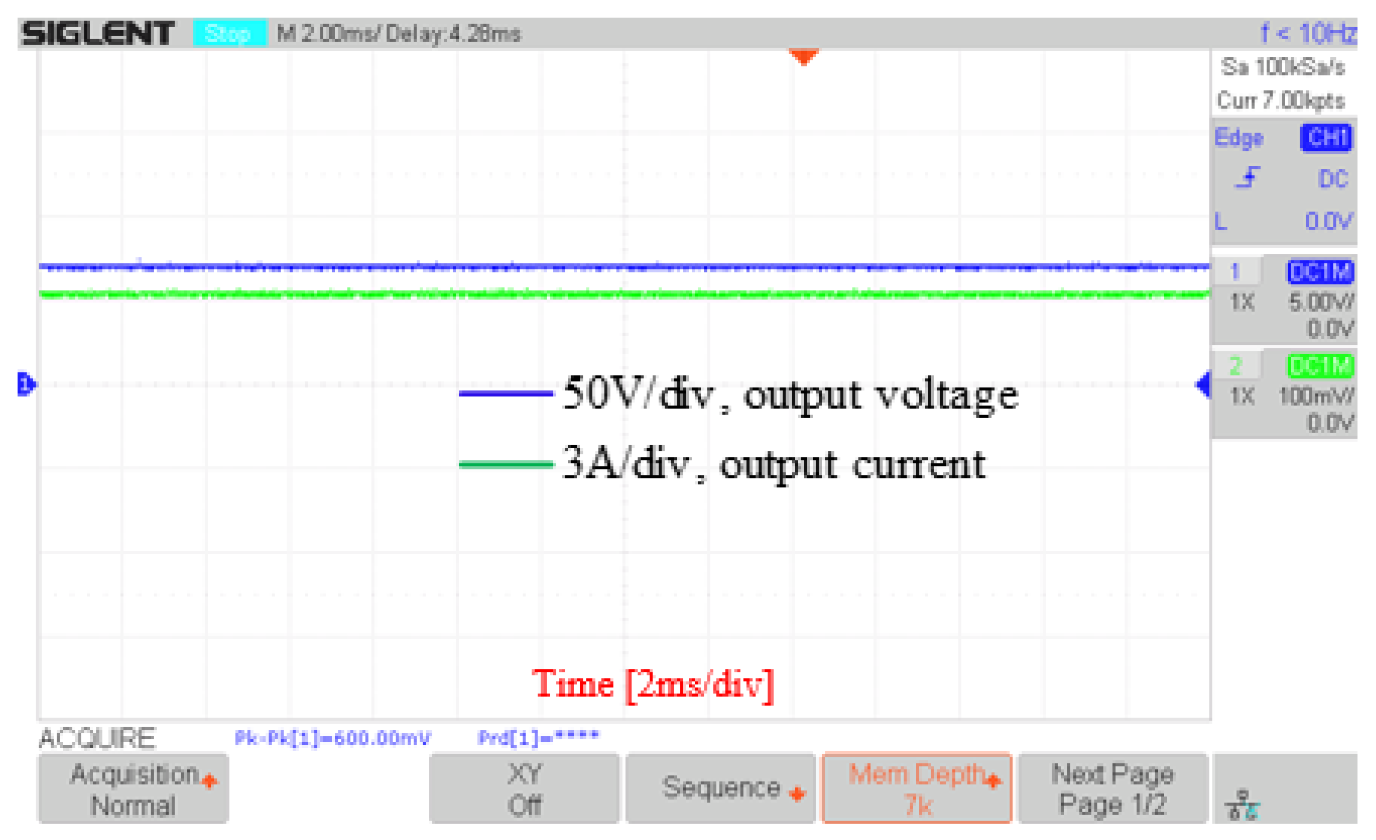
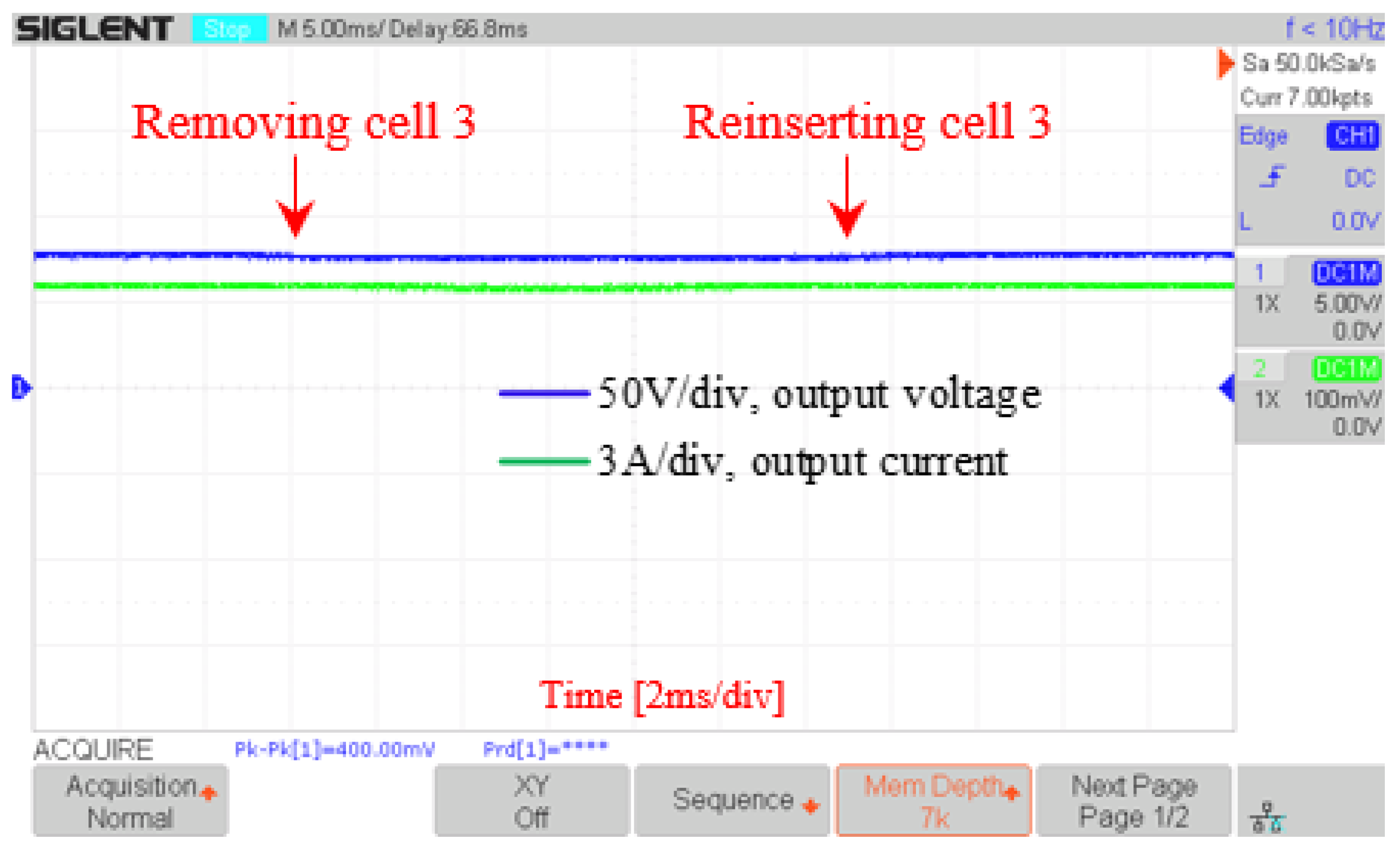
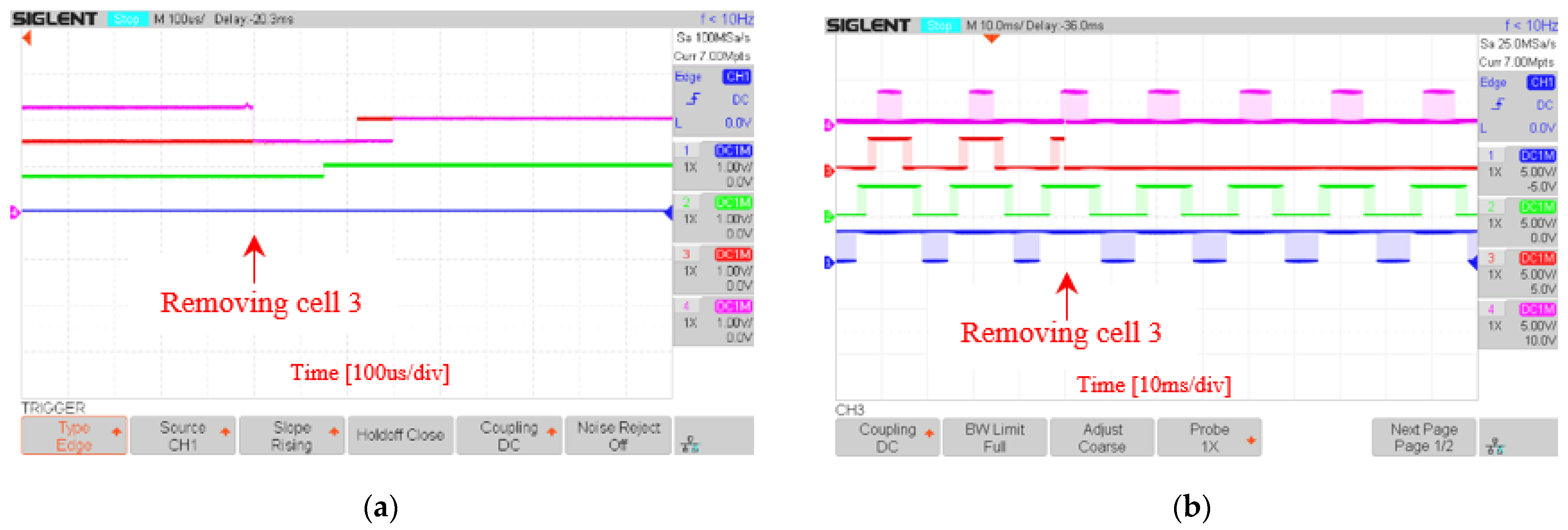
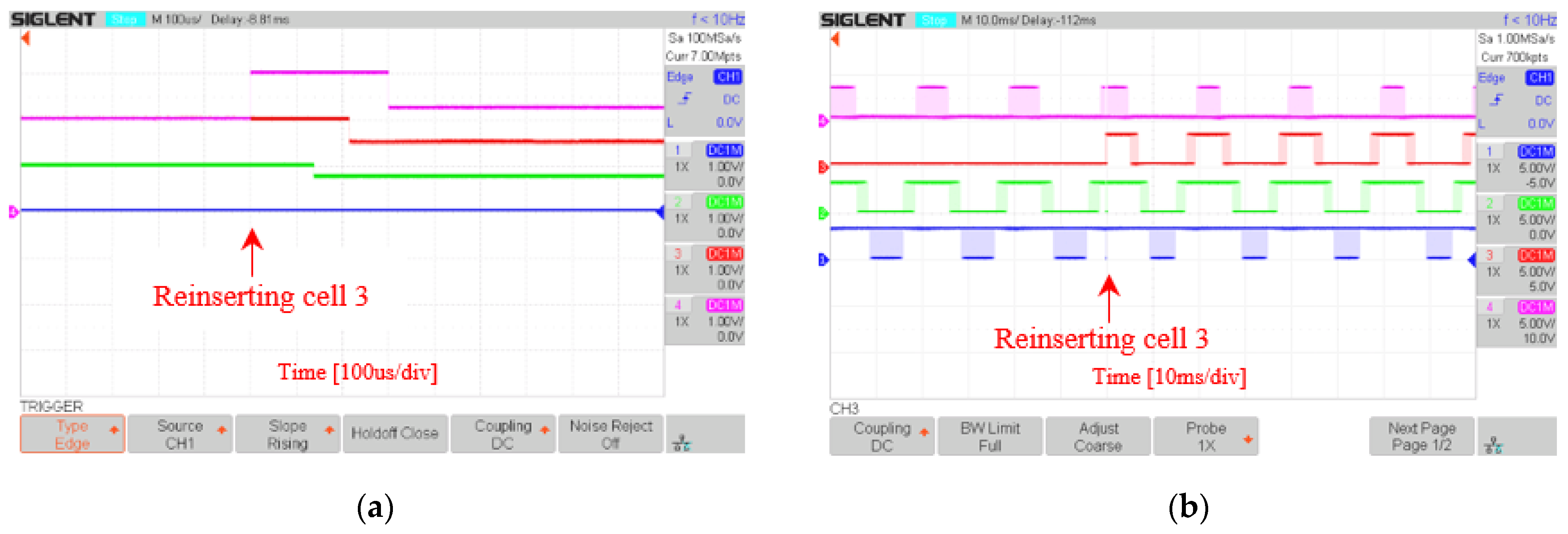
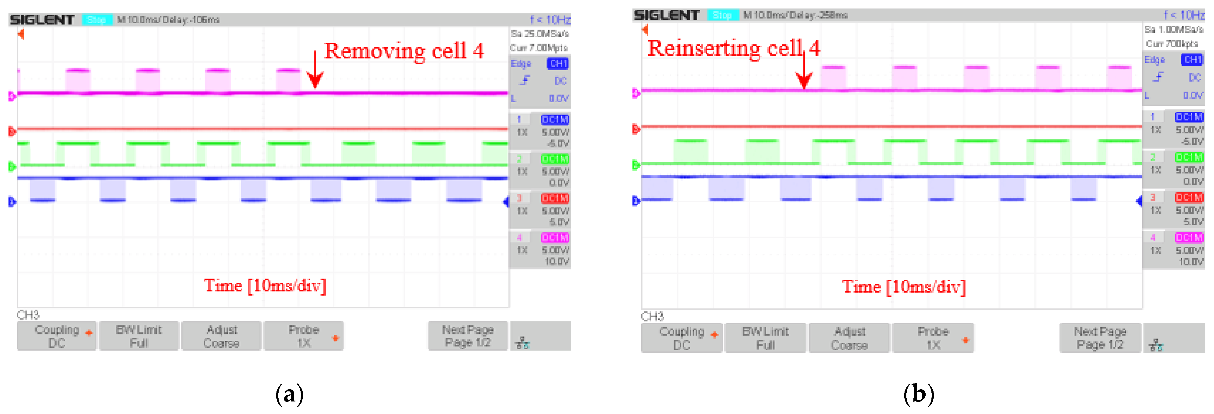
5.3. System Reconfiguration Speed

To compare the reconfiguration speed between the CPSC (modified updating rule) and the proposed DSA-PSC method, the transient system responses of a reconfiguration event when removing a cell (Figure 47) or reinserting a cell (Figure 48) for both methods are shown. It can be seen that using CPSC method, the reconfiguration system response takes around 250 µs, while this system response occurs within about 200 µs with the proposed DSA-PSC method. These measured system reconfiguration times are also similar to the simulation results, showing that DSA-PSC method is faster than the CPSC method.

6. Conclusions

In order to reduce the system configuration and reconfiguration times as well as to overcome some restrictions in updating rules of the conventional decentralized control method, two fast control methods are proposed in this paper, namely decentralized self-aligned phase-shifted carrier (DSA-PSC) and decentralized self-aligned level-shifted carrier (DSA-LSC). The algorithms of both methods are similar, where a cell controller sends to the next one the information of its angle/level, its index number, and the total number of activated cells of the converter. Then, each cell controller determines the inter-carrier phase-shift/elementary level shift and updates its own carrier-phase/carrier-level based on the received information. The proposed control algorithm can be easily implemented with DSP, can self-align the carriers rapidly and exactly, and can be applied to both phase-shifted and level-shifted multi-cell converters with any number of carriers. Simulation and experimental study are provided to validate the feasibility and the effectiveness of the proposed DSA-PSC and DSA-LSC methods.
It can be concluded that the main advantages of the proposed DSA-PSC and DSA-LSC are: (1) the system can operate with any number of carriers (N ≥ 1); (2) the system can start up from any value of carrier-phases or carrier-levels, including zero point; (3) in case a cell controller is inserted or removed, the system reaches the steady-state after predefined reconfiguration time (equal to 2N time steps); (4) the simulation study confirms that the reduction of configuration time is the key advantage of the proposed DSA-PSC method in comparison with the conventional decentralized phase-shifted method, and this reduction becomes more significant with higher number of carrier N; (5) simulation and experimental studies in case of a reconfiguration process for conventional and proposed methods also approve the advantages of the proposed DSA-PSC method in terms of lower reconfiguration time and zero inter-carrier phase-shifts relative error.

Author Contributions

All authors proposed and discussed the idea of this paper, performed the simulation, and implemented the experiment. All authors contributed to the writing of the manuscript, revised, and approved the final manuscript. All authors have read and agreed to the published version of the manuscript.

Funding

This research and the APC were funded by the Vietnam National University Ho Chi Minh City (VNU-HCM) under grant number B2019-20-07.

Acknowledgments

This research was funded by the Vietnam National University Ho Chi Minh City (VNU-HCM) under grant number B2019-20-07. We acknowledge the support of time and facilities from Ho Chi Minh City University of Technology (HCMUT), VNU-HCM for this study. We also thank Power Electronics Research LAB (HCMUT, VNU-HCM) and LAPLACE (INPT, Toulouse) for providing their precious collaboration.

Conflicts of Interest

The authors declare no conflict of interest.

References

  1. Costabeber, A.; Mattavelli, P.; Saggini, S. Digital Time-Optimal Phase Shedding in Multiphase Buck Converters. IEEE Trans. Power Electron. 2010, 25, 2242–2247. [Google Scholar] [CrossRef]
  2. Roh, Y.-S.; Moon, Y.-J.; Park, J.; Jeong, M.-G.; Yoo, C. A Multiphase Synchronous Buck Converter with a Fully Integrated Current Balancing Scheme. IEEE Trans. Power Electron. 2015, 30, 5159–5169. [Google Scholar] [CrossRef]
  3. Rodriguez, J.; Lai, J.-S.; Peng, F.Z. Multilevel inverters: A survey of topologies, controls, and applications. IEEE Trans. Ind. Electron. 2002, 49, 724–738. [Google Scholar] [CrossRef] [Green Version]
  4. Rodriguez, J.; Bernet, S.; Wu, B.; Pontt, J.; Kouro, S. Multilevel Voltage-Source-Converter Topologies for Industrial Medium-Voltage Drives. IEEE Trans. Ind. Electron. 2007, 54, 2930–2945. [Google Scholar] [CrossRef]
  5. Kouro, S.; Malinowski, M.; Gopakumar, K.; Pou, J.; Franquelo, L.G.; Wu, B.; Rodriguez, J.; Perez, M.A.; Leon, J.I. Recent Advances and Industrial Applications of Multilevel Converters. IEEE Trans. Ind. Electron. 2010, 57, 2553–2580. [Google Scholar] [CrossRef]
  6. Lesnicar, A.; Marquardt, R. An innovative modular multilevel converter topology suitable for a wide power range. In Proceedings of the 2003 IEEE Bologna Power Tech Conference Proceedings, Bologna, Italy, 23–26 June 2003; Volume 3, p. 6. [Google Scholar] [CrossRef]
  7. Akagi, H. Classification, Terminology, and Application of the Modular Multilevel Cascade Converter (MMCC). IEEE Trans. Power Electron. 2011, 26, 3119–3130. [Google Scholar] [CrossRef]
  8. Poblete, P.; Pereda, J.; Nunez, F.; Aguilera, R.P. Distributed Current Control of Cascaded Multilevel Inverters. In Proceedings of the 2019 IEEE International Conference on Industrial Technology (ICIT), Melbourne, Australia, 13–15 February 2019; pp. 1509–1514. [Google Scholar]
  9. Xia, B.; Li, Y.; Li, Z.; Konstantinou, G.; Xu, F.; Gao, F.; Wang, P. Decentralized Control Method for Modular Multilevel Converters. IEEE Trans. Power Electron. 2019, 34, 5117–5130. [Google Scholar] [CrossRef]
  10. Gateau, G.; Dung, P.; Cousineau, M.; Do, P.T.; Nhan, L.H.; Le, H.N. Digital implementation of decentralized control for multilevel converter. In Proceedings of the 2017 International Conference on System Science and Engineering (ICSSE), Ho Chi Minh City, Vietnam, 21–23 July 2017; pp. 558–562. [Google Scholar] [CrossRef]
  11. Xu, B.; Tu, H.; Du, Y.; Yu, H.; Liang, H.; Lukic, S. A Distributed Control Architecture for Cascaded H-Bridge Converter. In Proceedings of the 2019 IEEE Applied Power Electronics Conference and Exposition (APEC), Anaheim, CA, USA, 17–21 March 2019; pp. 3032–3038. [Google Scholar] [CrossRef]
  12. Liu, J.; Yao, W.; Lu, Z.; Du, L.; Ji, Y. A distributed control structure and synchronization method for complex converter based on CAN. In Proceedings of the 2017 IEEE Southern Power Electronics Conference (SPEC), Puerto Varas, Chile, 4–7 December 2017; pp. 1–6. [Google Scholar] [CrossRef]
  13. McGrath, B.P.; Holmes, D.G.; Kong, W.Y. A Decentralized Controller Architecture for a Cascaded H-Bridge Multilevel Converter. IEEE Trans. Ind. Electron. 2014, 61, 1169–1178. [Google Scholar] [CrossRef]
  14. Wang, P.; Tang, Y.; Tu, P.; Wang, P. A fault-tolerant operation scheme for a modular multilevel converter with a distributed control architecture. In Proceedings of the 2017 IEEE Energy Conversion Congress and Exposition (ECCE), Cincinnati, OH, USA, 1–5 October 2017; pp. 4163–4170. [Google Scholar] [CrossRef]
  15. Yang, S.; Tang, Y.; Zagrodnik, M.; Amit, G.; Wang, P. A novel distributed control strategy for modular multilevel converters. In Proceedings of the 2017 IEEE Applied Power Electronics Conference and Exposition (APEC), Tampa, FL, USA, 26–30 March 2017; pp. 3234–3240. [Google Scholar] [CrossRef]
  16. Liu, J.; Yao, W.; Lu, Z.; Ma, J. Design and implementation of a distributed control structure for modular multilevel matrix converter. In Proceedings of the 2018 IEEE Applied Power Electronics Conference and Exposition (APEC), San Antonio, TX, USA, 4–8 March 2018; pp. 1934–1939. [Google Scholar] [CrossRef]
  17. Burlacu, P.D.; Mathe, L.; Teodorescu, R. Synchronization of the distributed PWM carrier waves for modular multilevel converters. In Proceedings of the 2014 International Conference on Optimization of Electrical and Electronic Equipment (OPTIM), Bran, Romania, 22–24 October 2014; pp. 553–559. [Google Scholar] [CrossRef]
  18. Huang, S.; Mathe, L.; Teodorescu, R. A new method to implement resampled uniform PWM suitable for distributed control of modular multilevel converters. In Proceedings of the IECON 2013—39th Annual Conference of the IEEE Industrial Electronics Society, Vienna, Austria, 10–13 November 2013; pp. 228–233. [Google Scholar] [CrossRef]
  19. Rong, Y.; Wang, J.; Shen, Z.; Burgos, R.; Boroyevich, D.; Zhou, S. Distributed Control and Communication System for PEBB-based Modular Power Converters. In Proceedings of the 2019 IEEE Electric Ship Technologies Symposium (ESTS), Washington, DC, USA, 14–16 August 2019; pp. 627–633. [Google Scholar] [CrossRef]
  20. Sinha, M.; Poon, J.; Johnson, B.B.; Rodriguez, M.; Dhople, S.V. Decentralized Interleaving of Parallel-connected Buck Converters. IEEE Trans. Power Electron. 2019, 34, 4993–5006. [Google Scholar] [CrossRef]
  21. Dutta, S.; Mallik, R.; Majmunovic, B.; Mukherjee, S.; Seo, G.-S.; Maksimovic, D.; Johnson, B. Decentralized Carrier Interleaving in Cascaded Multilevel DC-AC Converters. In Proceedings of the 2019 20th Workshop on Control and Modeling for Power Electronics (COMPEL), Toronto, ON, Canada, 16–19 June 2019; pp. 1–6. [Google Scholar] [CrossRef]
  22. Phan, Q.D.; Gateau, G.; Nguyen, M.T.; Cousineau, M. 2D Decentralized Interleaving Principle for Multicell Serial-Parallel Converters. In Proceedings of the 2019 IEEE 13th International Conference on Power Electronics and Drive Systems (PEDS), Toulouse, France, 9–12 July 2019; pp. 1–7. [Google Scholar] [CrossRef]
  23. Cousineau, M.; le Bolloch, M.; Bouhalli, N.; Sarraute, E.; Meynard, T. Triangular carrier self-alignment using modular approach for interleaved converter control. In Proceedings of the 2011 14th European Conference on Power Electronics and Applications, Birmingham, UK, 30 August–1 September 2011; pp. 1–10. [Google Scholar]
  24. Xiao, Z.; Cousineau, M. Modular interleaved carrier generator using a straightforward implementation method. In Proceedings of the 2013 IEEE 11th International Workshop of Electronics, Control, Measurement, Signals and their application to Mechatronics, Toulouse, France, 24–26 June 2013; pp. 1–6. [Google Scholar] [CrossRef]
  25. Grégoire, L.-A.; Cousineau, M.; Seleme, I.S.; Ladoux, P. Real-Time Simulation of Interleaved Converters with Decentralized Control. In Proceedings of the International Conference on Renewable Energies and Power Quality (ICREPQ’16), Madrid, Spain, 4–6 May 2016; pp. 15–64. [Google Scholar]
  26. Gateau, G.; Cousineau, M.; Mannes-Hillesheim, M.; Dung, P. Digital Decentralized Current Control for Parallel Multiphase Converter. In Proceedings of the 2019 IEEE International Conference on Industrial Technology (ICIT), Melbourne, Australia, 13–15 February 2019; pp. 1761–1766. [Google Scholar] [CrossRef]
  27. Cousineau, M.; Xiao, Z. Fully decentralized modular approach for parallel converter control. In Proceedings of the 2013 Twenty-Eighth Annual IEEE Applied Power Electronics Conference and Exposition (APEC), Long Beach, CA, USA, 17–21 March 2013; pp. 237–243. [Google Scholar] [CrossRef]
  28. Cousineau, M.; Xiao, Z. Fully masterless control of parallel converter. In Proceedings of the 2013 15th European Conference on Power Electronics and Applications (EPE), Lille, France, 2–6 September 2013; pp. 1–10. [Google Scholar] [CrossRef]
  29. Seleme, S.I.; Gregoire, L.A.; Cousineau, M.; Ladoux, P. Modular control with carrier auto-interleaving and capacitor-voltage balancing for MMCs. IET Power Electron. 2019, 12, 817–828. [Google Scholar] [CrossRef]
  30. Gao, H.; Wang, Y. On Phase Response Function Based Decentralized Phase Desynchronization. IEEE Trans. Signal Process. 2017, 65, 5564–5577. [Google Scholar] [CrossRef]
  31. Sinha, M.; Dorfler, F.; Johnson, B.; Dhople, S. Stabilizing Phase-balanced or Phase-synchronized Trajectories of Van der Pol Oscillators in Uniform Electrical Networks. In Proceedings of the 2018 56th Annual Allerton Conference on Communication, Control, and Computing (Allerton), Monticello, IL, USA, 2–5 October 2018; pp. 335–340. [Google Scholar] [CrossRef]
  32. Duma, R.; Dobra, P.; Abrudean, M.; Dobra, M. Rapid prototyping of control systems using embedded target for TI C2000 DSP. In Proceedings of the 2007 Mediterranean Conference on Control & Automation, Athens, Greece, 27–29 June 2007; pp. 1–5. [Google Scholar] [CrossRef]
  33. Dos Santos, B.; Araujo, R.E.; Varajao, D.; Pinto, C. Rapid Prototyping Framework for real-time control of power electronic converters using simulink. In Proceedings of the IECON 2013—39th Annual Conference of the IEEE Industrial Electronics Society, Vienna, Austria, 10–13 November 2013; pp. 2303–2308. [Google Scholar] [CrossRef]
  34. Katzir, L.; Loewenstern, Y.; Bishara, B.; Shmilovitz, D. Implementation of a high voltage power supply with the MATLAB/Simulink embedded coder. In Proceedings of the 2014 IEEE 28th Convention of Electrical & Electronics Engineers in Israel (IEEEI), Eilat, Israel, 3–5 December 2014; pp. 1–4. [Google Scholar] [CrossRef]
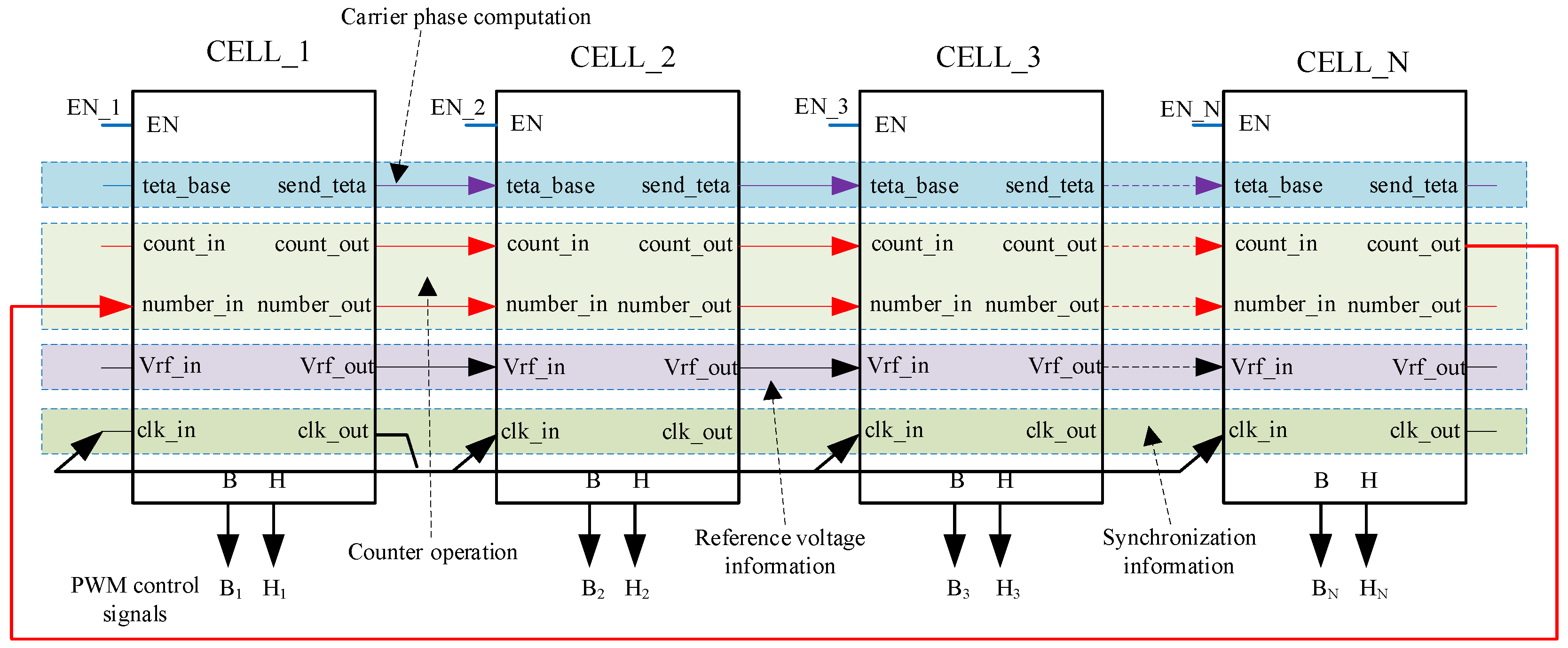
Figure 1. Multicellular converters, (a) multiphase converter [1,2]; (b) multilevel converter [3,4].
Applsci 11 00137 g001
Figure 2. Conventional decentralized method for multiphase converters, (a) intercellular communication; (b) basic iterative updating rule principle; (c) multiple reconfiguration.
Applsci 11 00137 g002aApplsci 11 00137 g002b
Figure 3. Analysis of convergence for a six-carriers system, (a) carrier phase; (b) inter-carrier phase-shift.
Applsci 11 00137 g003
Figure 4. Proposed update rule of phase-angle of carriers in decentralized self-aligned phase-shift (PS) carriers (DSA-PSC) method, (a) update rule principle; (b) phase-shifted carriers.
Applsci 11 00137 g004
Figure 5. Connection between each cell controller with the proposed DSA-PSC method.
Applsci 11 00137 g005
Figure 6. Algorithm flowchart of the proposed DSA-PSC method.
Applsci 11 00137 g006
Figure 7. Connection between each cell controller with the proposed decentralized self-aligned level-shifted carriers (DSA-LSC) method.
Applsci 11 00137 g007
Figure 8. Algorithm flowchart of the proposed DSA-LSC method.
Applsci 11 00137 g008
Figure 9. Proposed rule for the carrier level update with DSA-LSC method.
Applsci 11 00137 g009
Figure 10. Simulation model of the multiphase DC/DC converter (four phases), (a) topology; (b) connection between each cell controller.
Applsci 11 00137 g010aApplsci 11 00137 g010b
Figure 11. Simulation model of the multilevel DC/AC converter (five levels), (a) topology; (b) connection between each cell controller.
Applsci 11 00137 g011
Figure 12. Simulation result of four interleaved carriers using DSA-PSC method.
Applsci 11 00137 g012
Figure 13. PWM signals on the gates of the high-side switches (B1 … B4) of the converter cells.
Applsci 11 00137 g013
Figure 14. Output voltage, load current, and leg currents waveforms.
Applsci 11 00137 g014
Figure 15. Multiple reconfigurations of four interleaved carriers using DSA-PSC method, (a) carrier phases; (b) phase-shifted carriers.
Applsci 11 00137 g015
Figure 16. Simulation result of four level-shifted carriers using DSA-LSC method.
Applsci 11 00137 g016
Figure 17. PWM control signal at gates of the switches B1 … B4.
Applsci 11 00137 g017
Figure 18. Output voltage and output current waveforms.
Applsci 11 00137 g018
Figure 19. Reconfiguration of a four level-shifted carriers system.
Applsci 11 00137 g019
Figure 20. Output voltage waveform in a case of reconfiguration.
Applsci 11 00137 g020
Figure 21. Configuration time of conventional (modified updating rule) and proposed (DSA-PSC) self-aligned phase-shifted carrier methods.
Applsci 11 00137 g021
Figure 22. Configuration process of a converter with four-carriers, startup with (a) conventional modified updating rule; (b) proposed DSA-PSC.
Applsci 11 00137 g022
Figure 23. The inter-carrier phase-shifts of a converter with four-carriers, startup with (a) conventional modified updating rule; (b) proposed DSA-PSC.
Applsci 11 00137 g023
Figure 24. Configuration process of a converter with six-carriers, startup with (a) conventional modified updating rule; (b) proposed DSA-PSC.
Applsci 11 00137 g024
Figure 25. The inter-carrier phase-shifts of a converter with six-carriers, startup with (a) conventional modified updating rule; (b) proposed DSA-PSC.
Applsci 11 00137 g025
Figure 26. Configuration process of a converter with 13-carriers, startup with (a) conventional modified updating rule; (b) proposed DSA-PSC.
Applsci 11 00137 g026
Figure 27. The inter-carrier phase-shifts of a converter with 13-carriers, startup with (a) conventional modified updating rule; (b) proposed DSA-PSC.
Applsci 11 00137 g027
Figure 28. Multiple reconfigurations of six interleaved carriers using, (a) conventional phase-shifted carrier (CPSC) method (modified updating rule); (b) proposed DSA-PSC method.
Applsci 11 00137 g028aApplsci 11 00137 g028b
Figure 29. Experimental prototype for the test of the DSA-PSC and the DSA-LSC methods.
Applsci 11 00137 g029
Figure 30. System diagram for the experimentation of the DSA-PSC method.
Applsci 11 00137 g030
Figure 31. Experimental result of four interleaved carriers using DSA-PSC method, (a) carrier phases; (b) PWM control signals.
Applsci 11 00137 g031
Figure 32. Experimental result of three interleaved carriers using DSA-PSC method, (a) carrier phases; (b) PWM control signals.
Applsci 11 00137 g032
Figure 33. Experimental result of two interleaved carriers using DSA-PSC method, (a) carrier phases; (b) PWM control signals.
Applsci 11 00137 g033
Figure 34. The system response when removing cell 3, (a) carrier phases; (b) PWM control signals.
Applsci 11 00137 g034
Figure 35. The system response when reinserting cell 4, (a) carrier phases; (b) PWM control signals.
Applsci 11 00137 g035
Figure 36. Load voltage and load current waveforms when removing cell 3.
Applsci 11 00137 g036
Figure 37. Load voltage and load current waveforms when reinserting cell 3.
Applsci 11 00137 g037
Figure 38. System experimental diagram using DSA-LSC method.
Applsci 11 00137 g038
Figure 39. Experimental result of four interleaved carriers using DSA-LSC method, (a) carrier levels; (b) PWM control signals.
Applsci 11 00137 g039
Figure 40. The system response of restructuring when removing cell 3 by using DSA-LSC method, (a) carrier levels; (b) PWM control signals.
Applsci 11 00137 g040
Figure 41. The system response of restructuring when reinserting cell 3 by using DSA-LSC method, (a) carrier levels; (b) PWM control signals.
Applsci 11 00137 g041
Figure 42. Control signal of IGBT when removing and reinserting cell 4 by using DSA-LSC method, (a) PWM control signals; (b) PWM control signals.
Applsci 11 00137 g042
Figure 43. Experimental result of four level-shifted carriers using DSA-LSC method, (a) output voltage; (b) output current.
Applsci 11 00137 g043
Figure 44. Experimental results of three level-shifted carriers using DSA-LSC method, (a) output voltage; (b) output current.
Applsci 11 00137 g044
Figure 45. Output voltage and load current when removing and reinserting cell 3 using DSA-LSC method, (a) removing cell 3; (b) reinserting cell 3.
Applsci 11 00137 g045
Figure 46. FFT analysis of output voltage, (a) spectrum of nine first harmonics; (b) spectrum of 400 harmonics.
Applsci 11 00137 g046
Figure 47. Reconfiguration system response when removing cell 4, (a) conventional method; (b) proposed DSA-PSC method.
Applsci 11 00137 g047
Figure 48. Reconfiguration system response when reinserting cell 4, (a) conventional method; (b) proposed DSA-PSC method.
Applsci 11 00137 g048
Table 1. Input and output of cell model in DSA-PSC method.
InputOutput
ENEnable
teta_base θ n 1 k send_teta θ n k
count_inIndex from cell n−1, i n 1 k count_outIndex from cell n, i n k
number_inReceived total number from previous cells N t o t a l k number_outTransmitted total number to next cell N t o t a l k
Vrf_inReceived signal reference voltage from previous cellVrf_outTransmitted signal reference voltage to next cell
clk_inReceived synchronous clock pulse from master cellclk_outTransmitted synchronous clock pulse to other cell
Table 2. Input and output of cell controller with DSA-LSC method.
InputOutput
ENEnable
ampl_base A n 1 k ampl_min A n k
count_inIndex from cell n−1, i n 1 k count_outIndex from cell n, i n k
number_inReceived total number of cells N t o t a l k number_outTransmitted total number of cells to the next cell N t o t a l k
Vrf_inReceived modulation index of referenced voltage from the previous cellVrf_outTransmitted modulation index of referenced voltage to the next cell
Frf_inReceived referenced frequency from the previous cellFrf_outTransmitted frequency to the next cell
clk_inReceived synchronous clock pulse from the master cellclk_outTransmitted synchronous clock pulse to other cell
Table 3. Parameters of four-phase DC/DC converter.
ParameterSymbolUnitValue
Output inductorL1 … L4,
R1 … R4,
H
Ω
0.06
2.5
Load resistorRΩ20
Voltage sourceEV100
Switching frequencyfswkHz10
Sampling timeTss1 × 10−7
Duty_cycleD 0.8
Table 4. Parameters of five-level DC/AC converter.
ParameterSymbolUnitValue
Load resistorRΩ100
Voltage sourceVdc1 …… Vdc8V40
Switching frequencyfswkHz10
Sampling timeTss1 × 10−7
Modulation indexM 0.8
Table 5. Evaluate the system configuration time.
Number of Cells in the SystemConventional Modified Updating Rule
(K = 0.66; ε(Δθn, n+1) ≤ (10−4)0)
Proposed DSA-PSC Method
(ε(Δθn, n+1) = 00)
Number of time steps4148
62812
1317026
Table 6. Evaluate the system reconfiguration time for a six-cell converter.
ActionsConventional Modified Updating Rule
(K = 0.66; ε(Δθn, n+1) ≤ (10−4)0)
Proposed DSA-PSC Method
(ε(Δθn, n+1) = 00)
Number of time stepsRemoving cell 31710
Removing cell 5248
Reinserting cell 5158
Reinserting cell 32410
Table 7. Information on experimental components.
ComponentInformation
Controller board C2000 Delfino MCUs F28379D LaunchPad Development Kit, Texas Instruments, Dallas, TX, USA
Power circuit IGBT GW40N120KD
Driver circuitHybrid integrated IGBT driver MORNSUN QP12W08S-37, MORNSUN Guangzhou Science & Technology Co., Ltd.
Current sensor Current Transducer LTS 15-NP IPN = 15 At, LEM
Tektronix A622 AC/DC current probe
Table 8. Function of control pins of digital signal processor (DSP) for algorithm DSA-PSC.
ParameterPin on DSPFunction
count_inGPIO 97, 94, 65Get information of cell index from the previous cell
count_outGPIO 130, 63, 64Send information of cell index to the next cell
number_inGPIO 52, 41, 40Get information of total number of cell in the system
number_outGPIO 26, 27, 25Send information of total number of cell in the system
ENGPIO 66Enable to Activate/Deactivate the cell
clk_inGPIO 14Receive synchronous clock pulse
clk_outGPIO 04Send information of synchronous clock pulse to the next cell
teta_baseADCA15Get information of carrier phase angle from the previous cell
send_tetaDACBSend information of carrier phase angle to the next cell
Vrf_inADCA14Get information of modulation index of master cell
Vrf_outDACASend information of modulation index to orther cell
B signalGPIO 0IGBT control signal B (high-side switch)
H signalGPIO 1IGBT control signal H (low-side switch)
Table 9. Parameters of four-phase converter with algorithm DSA-PSC.
ParameterSymbolUnitValue
Output inductorL1 … L4,
R1 … R4,
H
Ω
0.06
2.5
Load resistorRΩ20
Voltage sourceEV100
Switching frequencyfswHz10,000
Sampling timeTss5 × 10−5
Duty cycleD 0.8
Table 10. Function of control pins of DSP for algorithm DSA-LSC.
ParameterPin on DSPFunction
count_inGPIO 97, 94, 65Get information of cell index from the previous cell
count_outGPIO 130, 63, 64Send information of cell index to the next cell
number_inGPIO 52, 41, 40Get information of total number of cells
number_outGPIO 26, 27, 25Send information of total number of cells
ENGPIO 66Enable to Activate/Deactivate a cell
clk_inGPIO 14Receive synchronous clock pulse
clk_outGPIO 04Send information of synchronous clock pulse to the next cell
Teta_baseADCA15Get information of phase from the previous cell
Send_tetaDACBSend information of phase to the next cell
Vrf_inADCA14Get information of modulation index from the previous cell
Vrf_outDACASend information of modulation index to the next cell
Frf_inGPIO 105, 104, 95, 139, 56, 10, 11Get information of frequency from the previous cell
Frf_outGPIO 29, 131, 05, 24, 16, 06, 07Send information of frequency to the next cell
B signalGPIO 0IGBT control signal B
H signalGPIO 1IGBT control signal H
Table 11. Parameters of five-level DC/AC converter with algorithm DSA-LSC.
ParameterSymbolUnitValue
Load resistorRΩ100
Voltage sourceVdc1 …… Vdc8V40
Switching frequencyfswHz10,000
Sampling timeTss5 × 10−5
Modulation indexM 0.8
Publisher’s Note: MDPI stays neutral with regard to jurisdictional claims in published maps and institutional affiliations.

