Data-Driven Modeling of Low Frequency Noise Using Capture-Emission Energy Maps

Department of System Semiconductor Engineering, Sangmyung University, Cheonan 31066, Korea
Appl. Sci. 2021, 11(1), 356; https://doi.org/10.3390/app11010356
Submission received: 13 November 2020
/
Revised: 23 December 2020
/
Accepted: 29 December 2020
/
Published: 31 December 2020
(This article belongs to the Section Electrical, Electronics and Communications Engineering)
Abstract
:A new approach for modeling low frequency noise is presented to enable the predictions of noise behavior from negative bias temperature instability (NBTI). The noise model is based on a capture-emission energy (CEE) map describing the probability density function of widely distributed defect capture-emission activation energies. To enlarge the capture-emission energy window and to perform the accurate estimation of the recoverable component of CEE, the Gaussian mixture model (GMM) is applied to the CEE map. This approach provides an efficient identification of noise sources and an in-depth noise analysis under both stationary and cyclo-stationary conditions.
1. Introduction
In nanoscale CMOS devices, the stochastic behavior of a few defects can have a significant impact on the reliability of devices and their circuits [1,2,3,4,5,6,7,8]. The negative bias temperature instability (NBTI) is among the most critical reliability issues and can be described by capture-emission energy (CEE) maps [3,4,5,9,10,11,12,13,14,15]. Accurately modeling the NBTI relies on a combined methodology comprising thorough CEE maps and efficient models. However, CEE maps are limited by the stress-recovery measurement window [9,10,14,15,16,17]. An accurate estimation of the parameters of CEE distribution is crucial to enable full lifetime calculation of NBTI without measurement time extrapolation. The kinetics of defects responsible for NBTI has been explained by the random capture-emission process of charge carriers caused by oxide traps [9,10,11,12,13,14,15,18,19]. Moreover, it has been found that the recoverable component of NBTI and random telegraph signal (RTS) noise are due to same defects [19,20,21,22,23,24,25]. The discrete fluctuations of RTSs with widely distributed time or energy scales are the main source of low frequency () noise in nanoscale MOSFETs [20,21,26,27,28,29]. For the statistical analysis and rigorous modeling of noise behavior, it is crucial to incorporate the distribution of defects based on CEE maps, including large signal AC operations [27,28,29,30]. In particular, since the static random-access memory (SRAM) cell is a highly scaled device, the threshold voltage variation due to RTS is a major source of degradation in SRAM characteristics [30]. In the CEE map framework, the time-dependent variability of degradation such as NBTI and noise is reproduced under different bias and duty cycle conditions. In this study, CEE-based noise models are newly presented to allow a quantitative prediction for RTS and noise. The models utilize a Gaussian mixture model (GMM) for enlarging the capture-emission energy window and clustering the recoverable component from the fitted CEE map.
2. Theoretical Model
The capture-emission process of charge carriers is consistent with non-radiative multi-phonon theory based on linear electron–phonon coupling [1]. In this theory, the capture-emission times are expressed as where is the temperature-independent pre-factor, is the Boltzmann constant, is the temperature, and and are the capture and emission activation energy, respectively. The NBTI-induced threshold voltage shifts is related to the capture-emission processes of individual defects with a broad distribution of characteristic times. The step height observed in for small-area devices is due to individual defects, while for large-area devices similar defects are grouped together using a suitable distribution of defects [1,19]. This distribution is visualized in the CEE map, which can be directly obtained from experimental recovery curves of for various stress conditions by using [1]. The defect density map is represented in agreement with bivariate Gaussian distribution, describing the permanent and recoverable components. In the activation energy space, the density is constructed by the joint probability density function [9,10,14,15]
where is a voltage-dependent amplitude with the stress voltage and the constants and . and are the mean values and standard deviations of , respectively. A correlation coefficient is defined as . For defects being charged up to the stress time and not yet being discharged at the recovery time , the threshold voltage shift is calculated by integrating over the activation energy map as follows [9,10,14,15]
where and are the recoverable and permanent component, respectively, and is the occupancy probability map for the applied stress and recovery waveform. The occupancy probability after and is described by [1]
For AC stress and recovery patterns with the signal duty cycle , and the signal frequency f, the probability to be occupied after the high gate-source voltage will be written as [30]
Trap-related processes are the most likely cause of the fluctuation in the number of charge carriers. The contribution of multiple-trap levels leads to a noise power spectrum expressed by the superposition of a single Lorentzian noise as follows [27]
where is the variance of the fluctuation in the number of carriers , is the amplitude, is the number of traps following a Poisson distribution, and is the angular frequency. With the assistance of capture-emission activation energies, a change in charge state can occur even if the energy levels of the traps are higher or lower than the Fermi level compared to a few , resulting in 1/f noise [31,32,33,34,35]. Assuming that is random variables identically distributed and the effective times constants are statistically independent, the noise power spectrum of the occupancy of the traps in the energy element and is given by [34,35]
where is the trap density per unit area. Given that the trap distribution is described by the normalized density of the recoverable component, the average noise power spectrum for a device with a width W and length L is converted to an integral expression
where is the effective time. Note that the term is similar to the occupancy of traps described by a Fermi function , reflecting the fact that traps with higher occupancy probability contribute to noise power. The equivalent gate voltage noise power spectrum of MOSFETs in the linear region is given by where is the gate oxide capacitance per unit area. Under cyclo-stationary square wave excitation, the noise behavior is governed by the time during the on-state, and , and the times during the off-state, and . The effective and characteristic times are written as [28]
with
For an accurate estimation of CEE distribution, a GMM of the distributions appears to be a natural choice for two components of Gaussian distributions. Given a two-dimensional random variable , with mean and covariance , the GM density function of two Gaussian components is given by [36,37,38,39]
where is the weight of the i-th mixture component, subject to and . The i-th independent normal distribution is
The expectation maximization (EM) algorithm is used to compute the parameters of each Gaussian component [36,37,38]. It is an iterative algorithm that estimates a maximum likelihood solution of the parameters, based on an expectation (E) step and a maximization (M) step. The GMM is used for clustering Gaussian components, by realizing that two bivariate Gaussian distributions of fitted CEE map can represent clusters. The soft clustering method is applied to estimate cluster membership posterior probabilities [39]. The method assigns a cluster membership score to each data point and ranks the points by their cluster membership score, allowing some data points to belong to multiple clusters.
3. Results and Discussion
The devices used for measurements were fabricated using a manufacturable remote plasma nitride oxide (RPNO) process. The gate oxide of devices used for measurements was grown with both furnace and rapid-thermal based processes. Following N2-plasma nitridation and post-nitridation anneal of the gate oxide, an undoped poly-Si gate layer was deposited. For p+ gates, B was implanted, and rapid-thermal annealing was then performed in N2 for different durations. The threshold voltage shifts are obtained on pMOSFETs (W = 10 , L = 0.14 , 2.2 nm), performing the ultrafast measure-stress-measurements [9,10]. With a measuring delay time of 1 , the temperature-accelerated measurement scheme was used to extend to the experimental stress-recovery window of . Noise measurements are conducted using an HP 3582A spectrum analyzer (1 Hz–25 kHz) and a Brookdeal 5004 low noise voltage amplifier connected at the output terminal. A bias resistance at the output terminal is chosen to be 10 times larger than the small signal channel resistance. The noise power spectrum is adjusted to subtract the noise due to the measurement system, which consists of the noise due to the amplifier and the bias resistance, and the thermal noise of device under test. Figure 1a shows experimental recovery data of following stress time with numerical data for and C. Numerical data of are obtained by integrating the CEE distribution in (2), which is calculated by taking the derivatives of measured data, as shown in Figure 1b. Figure 2a shows a scatter plot of GMM data using the soft clustering method. The cluster membership posterior probabilities in the interval (0.45,0.55) are members of both components with six shared data points. The estimated parameters of permanent component are eV, eV, eV, eV, and those of recoverable component are eV, eV, eV, eV, . Using the estimated parameters of GMM model, the CEE distributions are produced in the extended energy space exceeding experimental window, as observed in Figure 2b. The inset of Figure 2b shows a plot of the relative error values which are less than 0.5%.
To investigate how the trap distribution influences RTS noise, the integrand of for the recoverable component in (7) is numerically calculated and visualized as a function of and under stationary DC condition at a particular frequency. It is shown in Figure 3a that a peak is distinct at and for , and moves to relatively low activation energies and as the frequency increases to . As illustrated in the inset of Figure 3a, these results arise from different RTSs, indicating that faster components of shallow trap states for are situated close to lower activation energies [40]. To examine the behavior of cyclo-stationary RTS, the times are modeled as and , where the factor is assumed to be greater than one [28,40]. In the off state, and are multiplied and divided by , as they increase and decrease with a decrease in the gate voltage, respectively [28,40]. For a peak moves to higher emission energy , as shown in Figure 3b.
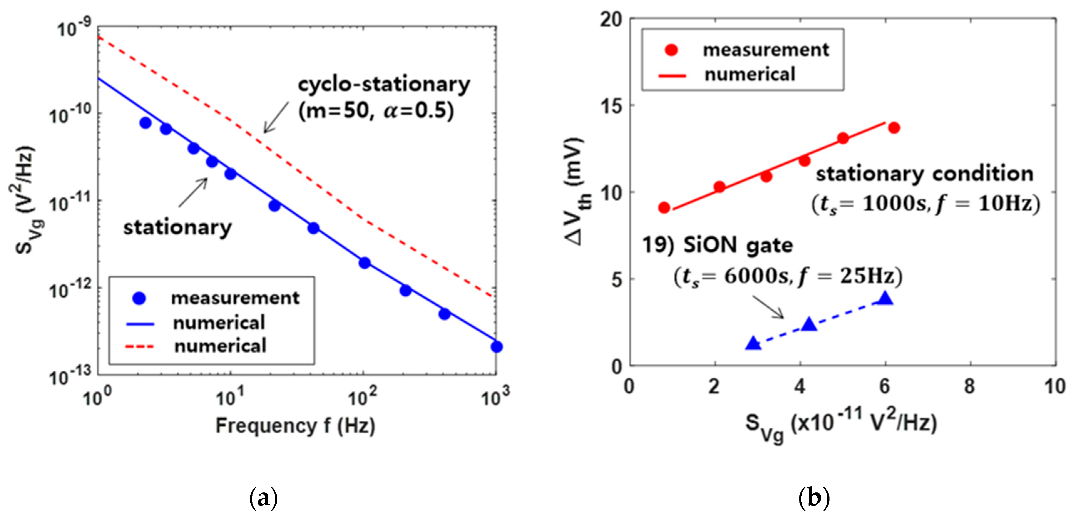
noise power is calculated by using (7) with the recoverable component obtained from GMM with soft clustering. It is observed in Figure 4a that the recoverable component of CEE map gives a spectrum form with a slope of −1. For asymmetric RTSs (, cyclo-stationary condition may lead to an increase in noise power [28]. Figure 4b shows a linear relationship between and after a stress time . The same strong correlation is also observed for the device with SiON/poly-Si gate [20].
4. Conclusions
In conclusion, with a recoverable component of NBTI stress-recovery, a new noise model is formulated based on a fitted CEE map with soft clustering of GMM. The proposed model offers the following unique features: (1) The model is based on the occupancy of defects in the capture-emission energy map. Therefore, it allows modeling of the noise under both stationary as well as cyclo-stationary excitation conditions. (2) The GMM with soft clustering enlarges the CEE window and performs independent estimations of two distinct components of CEE map, enabling the accurate calculation of noise characteristics. (3) New theoretical expressions can capture the noise behavior in terms of activation energies and provide the identification of noise sources and the reliable prediction of noise from NBTI.
Funding
This work was supported by the National Research Foundation of Korea (NRF) grant funded by the Korea government (MSIT) (No. 2019R1F1A1050640).
Data Availability Statement
No new data were created or analyzed in this study. Data sharing is not applicable to this article.
Conflicts of Interest
The author declares no conflict of interest.
References
- Grasser, T. Stochastic charge trapping in oxides: From random telegraph noise to bias temperature instabilities. Microelectron. Reliab. 2012, 52, 39–70. [Google Scholar] [CrossRef]
- Grasser, T.; Kaczer, B.; Goes, W.; Reisinger, H.; Aichinger, T.; Hehenberger, P.; Wagner, P.-J.; Schanovsky, F.; Franco, J.; Luque, M.T.; et al. The Paradigm Shift in Understanding the Bias Temperature Instability: From Reaction–Diffusion to Switching Oxide Traps. IEEE Trans. Electron Devices 2011, 58, 3652–3666. [Google Scholar] [CrossRef]
- Reisinger, H.; Grasser, T.; Gustin, W.; Schlünder, C. The statistical analysis of individual defects constituting NBTI and its implications for modeling DC- and AC-stress. In Proceedings of the 2010 IEEE International Reliability Physics Symposium, Anaheim, CA, USA, 2–6 May 2010; pp. 7–15. [Google Scholar]
- Reisinger, H.; Grasser, T.; Schlünder, C. A study of NBTI by the statistical analysis of the properties of individual defects in pMOSFETs. In Proceedings of the 2009 IEEE International Integrated Reliability Workshop Final Report, South Lake Tahoe, CA, USA, 18–22 October 2009; pp. 30–35. [Google Scholar]
- Reisinger, H.; Blank, O.; Heinrigs, W.; Gustin, W.; Schlünder, C. A comparison of very fast to very slow components in degradation and recovery due to NBTI and bulk hole trapping to existing physical models. IEEE Trans. Device Mater. Reliab. 2007, 7, 119–129. [Google Scholar] [CrossRef]
- Reisinger, H.; Grasser, T.; Ermisch, K.; Nielen, H.; Gustin, W.; Schlünder, C. Understanding and modeling AC BTI. In Proceedings of the 2011 IEEE International Reliability Physics Symposium, Monterey, CA, USA, 10–14 April 2011; pp. 597–604. [Google Scholar]
- Bucolo, M.; Buscarino, A.; Famoso, C.; Fortuna, L.; Frasca, M. Control of imperfect dynamical systems. Nonlinear Dyn. 2019, 98, 2989–2999. [Google Scholar] [CrossRef]
- Zhao, K.; Stathis, J.H.; Linder, B.P.; Cartier, E.; Kerber, A. PBTI under dynamic stress: From a single defect point of view. In Proceedings of the 2011 IEEE International Reliability Physics Symposium, Monterey, CA, USA, 10–14 April 2011; pp. 372–380. [Google Scholar]
- Puschkarsky, K.; Reisinger, H.; Schlünder, C.; Gustin, W.; Grasser, T. Voltage-dependent activation energy maps for analytic lifetime modeling of NBTI without time extrapolation. IEEE Trans. Electron Devices 2018, 65, 4764–4771. [Google Scholar] [CrossRef]
- Puschkarsky, K.; Reisinger, H.; Rott, G.A.; Schlünder, C.; Gustin, W.; Grasser, T. An efficient analog compact NBTI model for stress and recovery based on activation energy maps. IEEE Trans. Electron Devices 2019, 66, 4623–4630. [Google Scholar] [CrossRef]
- Giering, K.U.; Puschkarsky, K.; Reisinger, H.; Rzepa, G.; Rott, G.; Vollertsen, R.; Grasser, T.; Jancke, R. NBTI degradation and recovery in analog circuits: Accurate and efficient circuit-level modeling. IEEE Trans. Electron Devices 2019, 66, 1662–1668. [Google Scholar] [CrossRef]
- Ma, C.; Mattausch, H.J.; Matsuzawa, K.; Yamaguchi, S.; Hoshida, T.; Imade, M.; Koh, R.; Arakawa, T.; Miura-Mattausch, M. Universal NBTI compact model for circuit aging simulation under any stress conditions. IEEE Trans. Device Mater. Reliab. 2014, 14, 818–825. [Google Scholar] [CrossRef]
- Wang, W.; Yang, S.; Bhardwaj, S.; Vrudhula, S.; Liu, F.; Cao, Y. The impact of NBTI effect on combinational circuit: Modeling, simulation, and analysis. IEEE Trans. Very Large Scale Integr. VLSI Syst. 2009, 18, 173–183. [Google Scholar] [CrossRef]
- Lagger, P.; Reiner, M.; Pogany, D.; Ostermaier, C. Comprehensive study of the complex dynamics of forward bias-induced threshold voltage drifts in GaN based MIS-MEMTs by stress/recovery experiments. IEEE Trans. Electron Devices 2014, 61, 1022–1030. [Google Scholar] [CrossRef]
- Putcha, V.; Franco, J.; Vais, A.; Sioncke, S.; Kaczer, B.; Linten, D.; Groeseneken, G. On the apparent non-Arrhenius temperature dependence of charge trapping in IIIV/high-k MOS stack. IEEE Trans. Electron Devices 2018, 65, 3689–3696. [Google Scholar] [CrossRef]
- Pobegen, G.; Grasser, T. On the distribution of NBTI time constants on a long, temperature-accelerated time scale. IEEE Trans. Electron Devices 2013, 60, 2148–2155. [Google Scholar] [CrossRef]
- Pobegen, G.; Aichinger, T.; Nelhiegbel, M.; Grasser, T. Understanding temperature acceleration for NBTI. In Proceedings of the 2011 International Electron Device Meeting, Washington, DC, USA, 5–7 December 2011; pp. 614–617. [Google Scholar]
- Tewksbury, T.L.; Lee, H.S. Characterization, modeling, and minimization of transient threshold voltage shifts in MOSFET’s. IEEE J. Solid State Circuits 1994, 29, 239–252. [Google Scholar] [CrossRef]
- Grasser, T.; Rott, K.; Reisinger, H.; Waltl, M.; Franco, J.; Kaczer, B. A unified perspective of RTN and BTI. In Proceedings of the 2014 IEEE International Reliability Physics Symposium, Waikoloa, HI, USA, 1–5 June 2014; pp. 4A.5.1–4A.5.7. [Google Scholar]
- Kaczer, B.; Grasser, T.; Martin-Martinez, J.; Simoen, E.; Aoulaiche, M.; Roussel, P.J.; Groseneken, G. NBTI from the perspective of defect states with widely distributed time scales. In Proceedings of the 2009 IEEE International Reliability Physics Symposium, Montreal, QC, Canada, 26–30 April 2009; pp. 55–60. [Google Scholar]
- Huard, V. Two independent components modeling for negative bias temperature instability. In Proceedings of the 2010 IEEE International Reliability Physics Symposium, Anaheim, CA, USA, 2–6 May 2010; pp. 33–42. [Google Scholar]
- Tsukamoto, Y.; Toh, S.O.; Shin, C.; Mairena, A.; Liu, T.-J.K.; Nikolic, B. Analysis of the relationship between random telegraph signal and negative bias temperature instability. In Proceedings of the 2010 IEEE International Reliability Physics Symposium, Anaheim, CA, USA, 2–6 May 2010; pp. 1117–1121. [Google Scholar]
- Bury, E.; Degraeve, R.; Cho, M.J.; Kaczer, B.; Goes, W.; Grasser, T.; Horiguchi, N.; Groeseneken, G. Study of (correlated) trap sites in SILC, BTI and RTN in SiON and HKMG devices. In Proceedings of the 21th International Symposium on the Physical and Failure Analysis of Integrated Circuits (IPFA), Marina Bay Sands, Singapore, 30 June–4 July 2014; pp. 250–253. [Google Scholar]
- Both, T.H.; Furtado, G.F.; Wirth, G.I. Modeling and simulation of the charge trapping component of BTI and RTS. Microelectron. Reliab. 2018, 80, 278–283. [Google Scholar] [CrossRef]
- Wirth, G.I.; da Silva, R.; Kaczer, B. Statistical model for MOSFET bias temperature instability component due to charge trapping. IEEE Trans. Electron Devices 2011, 58, 2743–2751. [Google Scholar] [CrossRef]
- Grasser, T.; Reisinger, H.; Goes, W.; Aichinger, T.; Hehenberger, P.; Wagner, P.J.; Nelhiebel, M.; Franco, J.; Kaczer, B. Switching oxide traps as the missing link between negative bias temperature instability and random telegraph noise. In Proceedings of the 2009 International Electron Device Meeting, Baltimore, MD, USA, 7–9 December 2009; pp. 729–732. [Google Scholar]
- Da Silva, R.; Wirth, G.; Brusamarello, L. An appropriate model for the noise power spectrum produced by traps at the Si–SiO2 interface: A study of the influence of a time-dependent Fermi level. J. Stat. Mech. Theory Exp. 2008, 2008, P10015. [Google Scholar] [CrossRef]
- Wirth, G.; da Silva, R. Low-frequency noise spectrum of cyclo-stationary random telegraph signals. Electr. Eng. 2008, 90, 435–441. [Google Scholar] [CrossRef]
- Da Silva, R.; Wirth, G.I.; Brederlow, R. Novel analytical and numerical approach to modeling low-frequency noise in semiconductor devices. Phys. A Stat. Mech. Appl. 2006, 362, 277–288. [Google Scholar] [CrossRef]
- Weckx, P.; Kaczer, B.; Toledano-Luque, M.; Grasser, T.; Roussel, P.J.; Kukner, H.; Raghavan, P.; Catthoor, F.; Groeseneken, G. Defect-based methodology for workload-dependent circuit lifetime projections-Application to SRAM. In Proceedings of the 2013 IEEE International Reliability Physics Symposium, Anaheim, CA, USA, 14–18 April 2013; pp. 3A.4.1–3A.4.7. [Google Scholar]
- Fleetwood, D.M. 1/f noise and defects in microelectronic materials and devices. IEEE Trans. Nucl. Sci. 2015, 62, 1462–1486. [Google Scholar] [CrossRef]
- Fleetwood, D.M.; Xiong, H.D.; Lu, Z.Y.; Nicklaw, C.J.; Felix, J.A.; Schrimpf, R.D.; Pantelides, S.T. Unified model of hole trapping, 1/f noise, and thermally stimulated current in MOS devices. IEEE Trans. Nucl. Sci. 2002, 49, 2674–2683. [Google Scholar] [CrossRef]
- Simoen, E.; Claeys, C. On the flicker noise in submicron silicon MOSFETs. Solid-State Electron. 1999, 43, 865–882. [Google Scholar] [CrossRef]
- Wong, H.; Cheng, Y.C. Modeling of low-frequency noise in metal-oxide-semiconductor field-effect transistor with electron trapping-detrapping at oxide-silicon interface. IEEE Trans. Electron Devices 1991, 38, 1883–1888. [Google Scholar] [CrossRef]
- Surya, C.; Hsiang, T.Y. A thermal activation model for 1/ƒy noise in Si-MOSFETs. Solid State Electron. 1988, 31, 959–964. [Google Scholar] [CrossRef]
- Shimizu, H.; Awano, H.; Hiromoto, M.; Sato, T. Automation of model parameter estimation for random telegraph noise. IEICE Trans. Fundam. Electron. Commun. Comput. Sci. 2014, E97-A, 2383–2392. [Google Scholar] [CrossRef] [Green Version]
- Singh, R.; Pal, B.C.; Jabr, R.A. Statistical representation of distribution system loads using Gaussian mixture model. IEEE Trans. Power Syst. 2010, 25, 29–37. [Google Scholar] [CrossRef] [Green Version]
- Bui, D.T.; Hoang, N.D. A Bayesian framework based on a Gaussian mixture model and radial-basis-function Fisher discriminant analysis (BayGmmKda V1.1) for spatial prediction of floods. Geosci. Model Dev. 2017, 10, 3391–3409. [Google Scholar] [CrossRef] [Green Version]
- Peters, G.; Crespo, F.; Lingras, P.; Weber, R. Soft clustering—Fuzzy and rough approaches and their extensions and derivatives. Int. J. Approx. Reason. 2013, 54, 307–322. [Google Scholar] [CrossRef]
- van der Wel, A.P.; Klumperink, E.A.M.; Hoekstra, E.; Nauta, B. Relating random telegraph signal noise in metal-oxide-semiconductor transistors to interface trap energy distribution. Appl. Phys. Lett. 2005, 87, 183507. [Google Scholar] [CrossRef] [Green Version]
Figure 1.
Threshold voltage shifts and capture-emission energy (CEE) map. (a) Numerical data with measured data of . (b) Comparison of numerical data with measured data of CEE map.
Figure 1.
Threshold voltage shifts and capture-emission energy (CEE) map. (a) Numerical data with measured data of . (b) Comparison of numerical data with measured data of CEE map.

Figure 2.
CEE map with fitted Gaussian mixture (GMM) using soft clustering. (a) Scatter plot of GMM data. (b) Comparison of GMM data with numerical data of CEE map.
Figure 2.
CEE map with fitted Gaussian mixture (GMM) using soft clustering. (a) Scatter plot of GMM data. (b) Comparison of GMM data with numerical data of CEE map.
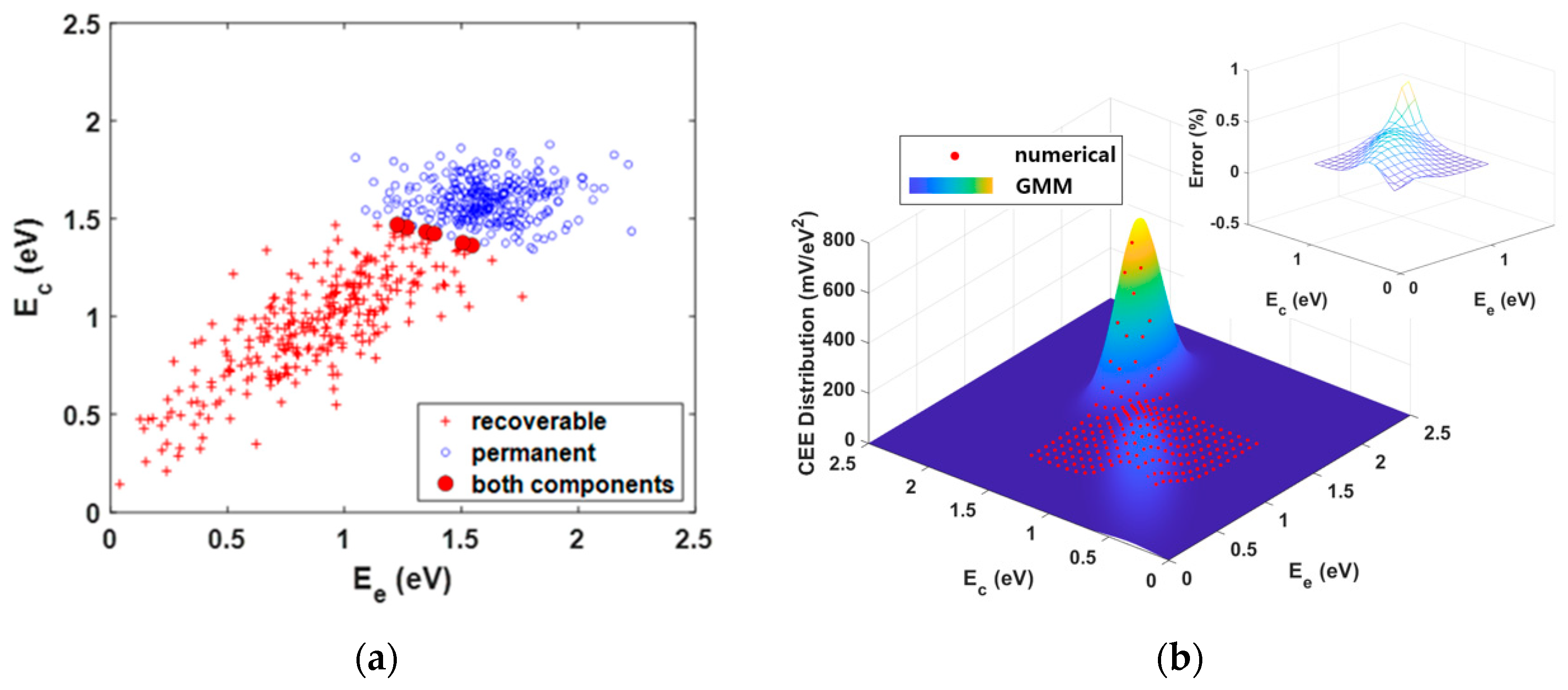
Figure 3.
Integrand of for the recoverable component. (a) f = 1 Hz and f = 1 kHz under stationary condition for . (b) f = 1 Hz and m = 50 under cyclo-stationary condition for .
Figure 3.
Integrand of for the recoverable component. (a) f = 1 Hz and f = 1 kHz under stationary condition for . (b) f = 1 Hz and m = 50 under cyclo-stationary condition for .

Figure 4.
1/f noise spectrum and threshold voltage shifts for . (a) for , (b) versus for .
Publisher’s Note: MDPI stays neutral with regard to jurisdictional claims in published maps and institutional affiliations. |
© 2020 by the author. Licensee MDPI, Basel, Switzerland. This article is an open access article distributed under the terms and conditions of the Creative Commons Attribution (CC BY) license (http://creativecommons.org/licenses/by/4.0/).
Share and Cite
MDPI and ACS Style
Lee, J. Data-Driven Modeling of Low Frequency Noise Using Capture-Emission Energy Maps. Appl. Sci. 2021, 11, 356. https://doi.org/10.3390/app11010356
AMA Style
Lee J. Data-Driven Modeling of Low Frequency Noise Using Capture-Emission Energy Maps. Applied Sciences. 2021; 11(1):356. https://doi.org/10.3390/app11010356
Chicago/Turabian StyleLee, Jonghwan. 2021. "Data-Driven Modeling of Low Frequency Noise Using Capture-Emission Energy Maps" Applied Sciences 11, no. 1: 356. https://doi.org/10.3390/app11010356
Note that from the first issue of 2016, this journal uses article numbers instead of page numbers. See further details here.