A New Circuit Design of AC/DC Converter for T8 LED Tube


1
Electrical Engineering Department, Inha University, 100 Inharo, Nam-gu Incheon 22212, Korea
2
Fire and Disaster Prevention Department, Semyung University, 65 Semyung-ro, Jecheon-si, Chungcheongbuk-do 27136, Korea
*
Author to whom correspondence should be addressed.
Appl. Sci. 2021, 11(1), 421; https://doi.org/10.3390/app11010421
Submission received: 25 November 2020
/
Revised: 14 December 2020
/
Accepted: 18 December 2020
/
Published: 4 January 2021
(This article belongs to the Special Issue Light Emitting Diode)
Abstract
:This study is about an improved high-quality light-emitting diode (LED) converter for a T8 LED tube. The converter is separated into the AC driving circuit and DC driving circuit. Also, the LED tube was applied with an output ripple eliminator for the optical performance. The AC driving circuit and DC driving circuit are assembled at the end of the LED tube in a G13 base and a G13 base dummy, respectively, and the output ripple eliminator is located on an LED PCB. The proposed LED converter is founded on a SSBB (single-stage buck-boost) converter topology and was designed for 10 W operation for a 600 mm T8 LED tube. The light waveform of the LED tube was measured by a photosensor. The waveform had almost no ripple and was the same as a straight line. The average calculated percent flicker of the proposed LED converter was an average of 1.9% at 100 and 240 VAC, 50 and 60 Hz. The proposed converter has lower power efficiency than a conventional converter by 2.7% at 100–240 VAC, but it still has high power efficiency (>87%). The measurement results represent that the LED output current regulation is below 0.92% at 100–240 VAC and the converter obtains the power factor more than 0.84 and the total harmonic distortion is less than 14.3%. All of the current harmonics reach the IEC 61000-3-2 Class D standards for high-quality LED converters.
1. Introduction
LEDs have a lot of characteristics such as high luminous efficacy, energy saving properties and long lifetimes. These advantages have allowed LED lighting to replace other types of lighting quickly in the marketplace. Furthermore, as regulations for the use of traditional lighting such as incandescent lamps and florescent lamps become increasingly stronger, the market share of LED lighting is expected to increase rapidly [1,2,3].
An LED lighting product generally consists of various mechanical parts, an LED module and an LED converter. An LED converter should provide stable and accurate current to the LED module to achieve good optical performance, since the luminance variation of LEDs depends on the variation of the current supplied to LEDs. In addition, the LED converter requires high power efficiency, high power factor (PF), low total harmonic distortion (THD), low total cost, and low light flicker [4,5].
The light quality of LED lighting is mainly determined by the driving method and the key components of the LED converter. Due to the low circuit complexity and low cost, a single-stage power factor correction (PFC) driving method is usually used in many types of low-power LED lightings, including LED tubes. However, the output current inevitably has a double line frequency ripple and light flicker is generated by variation of the luminance. Various studies show that low-frequency light flicker caused by large output current ripple can adversely affect human health and cause headaches, visual fatigue and epileptic attacks [6,7,8,9].
Figure 1 shows a block diagram of a typical single-stage buck-boost LED converter, which is composed of many function blocks. An AC voltage with 50/60 Hz is supplied to a bridge rectifier through a line filter, and a full-wave rectified sinusoidal voltage is supplied to the DC link capacitor CLINK. Switching is conducted for power factor correction to obtain high power factor, and smoothing is performed to reduce the output ripple and control the output current [5].
The smoothing to remove the ripple is not perfect, so the single-stage PFC driving method always makes a low-frequency output ripple, and output current varies between a maximum peak and minimum peak [10]. If the light has cyclic variation in the amplitude, percent flicker is very useful to represent the level of light flicker, which is defined as [11]:
where A and B are the maximum and minimum luminance, respectively. The Equation (1) shows that the low percent flicker represents good performance. Several methods can be considered to improve the light flicker caused by the double line frequency output ripple [12,13,14,15]. One of the obvious ways is to increase the link capacitor CDC; however, regulatory requirements for PF and THD performance may not be met. Therefore, this method is usually suitable for non-regulated low power LED lighting. Another method is to increase the output capacitance for the smoothing operation. However, a large electrolytic capacitor is needed to remove the output ripple completely, which increases the system size and cost. Therefore, this is not suitable for small lighting applications with small circuit space. Various converter topologies have been proposed to remove current ripple [16,17,18]. In [16], a flicker-free LED converter composed of PFC flyback converter and a bidirectional buck/boost converter to reduce the current ripple was proposed to reduce the current ripple. The output current waveform is almost flat, while high power efficiency is maintained [16,17].
However, due to the high circuit complexity, it cannot be applied to applications such as T8 LED tubes. A multiplexing ripple cancellation was proposed by adding a ripple cancellation unit to achieve flicker-free operation in [18]. Although this solution is very competitive, it is still too large to mount inside a G13 base with a diameter of 28 mm for low-power LED tubes [19]. In this paper, an LED converter with an output ripple eliminator is proposed to remove the double line frequency flicker of a T8 LED tube, while providing high power efficiency, high PF, low THD and precise output current regulation. Due to the addition of the output ripple eliminator, the power efficiency has been slightly reduced by an average of 2.7%. Nevertheless, the power efficiency is still more than 87% and light flicker is almost removed. The proposed LED converter is separated into AC and DC driving circuit and designed to mount in a G13 base and G13 base dummy. Because of the size limitations, we propose a practical method for product manufacturing by locating the output ripple eliminator on the LED module. In Section 2, the theory of the output ripple eliminator operation is explained. In Section 3, design specifications of the proposed LED converter are represented in detail. In Section 4, a 10 W prototype is introduced and experimental results are discussed. Finally, conclusions are given in Section 5.
2. The Proposed LED Converter for a T8 LED Tube
2.1. Power Stage
Figure 2a shows the overall stages of the proposed LED converter, which consists of a power stage for constant current control and a ripple remove stage to reduce the output ripple. The power stage is physically divided into two driving circuit that are electrically linked though the LED module [5]. Figure 2b shows a simplified circuit diagram of the proposed LED converter with separated driving circuit for a T8 LED tube.
The proposed LED converter employs a single-stage buck-boost converter topology and consists of an AC driving circuit for rectification and a DC driving circuit for constant current control. The AC driving circuit consists of various filter components (CX, LF) for high frequency suppression, a full bridge rectifier (BD) and a DC link capacitor (CLINK1). The DC driving circuit includes another DC link capacitor (CLINK2), a power switch for energy transfer (S), an inductor (L), a diode (D) and an output capacitor (CO) [5,20]. The full bridge rectifier generates a positive full wave sinusoidal voltage from the AC line and supplies it to the DC link capacitor in the AC driving circuit. The inductor is magnetized and stores rectified input energy from the AC driving circuit when the switch S turns on.
During the turn-off time, the inductor is demagnetized, and stored energy is transferred to the output capacitor. In the single-stage driving method, the input voltage can be defined as:
where is the amplitude of the input voltage and is the line frequency of the input voltage. Since the controller is operated for power factor correction, the input current waveform follows the input voltage waveform. Therefore, the input current is defined as:
where is the peak value of the input current. From Equations (1) and (2), the instantaneous output power can be expressed as [5,21]:
where is the expected power efficiency and is substituted with the amplitude of the output power . When is the output voltage, the instantaneous output current can be expressed as:
where is the amplitude of the output current. The equation (5) shows that the single-stage power factor correction driving method always contains double line frequency output ripple. If the output capacitance does not sufficiently smooth the output ripple, the high and low amplitude current flowing through the LEDs generates light flicker [5,21,22,23].
2.2. Ripple Free Stage
Figure 3 shows the output ripple eliminator of the proposed LED converter for alleviating light flicker. An output ripple eliminator is a kind of common collector amplifier using an NPN Darlington configuration, which is one of the basic amplifier topologies, as a voltage follower. It consists of , , and a Darlington transistor [24,25].
Since the bias voltage of the base is immediately transferred to the LED anode, the impedance should be carefully chosen to find the optimized LED operation point in terms of power losses and light flicker elimination.
Figure 4 shows conceptual waveforms of the proposed output ripple eliminator. To achieve a high power factor of the proposed LED converter, the output waveform inevitably contains a large ripple with double line frequency. This double frequency ripple is passed through the power stage and transferred to the ripple removal stage. Since the output voltage is constant with output ripple, it can be expressed as:
where and are the DC component and AC component with double line frequency ripple, respectively. Therefore, the base bias voltage of the Darlington pair has the same frequency ripple in steady state and the instantaneous value of bias voltage can be expressed as:
where and are the DC component and AC component of the collector-base forward voltage, respectively. Considering the base-emitter forward voltage in the Darlington input stage, applied across LEDs can be obtains as:
where is the DC value, and is the AC value. Using Kirchhoff’s voltage law, the AC component of bias voltage is determined from , and ,
where is the total impedance, and is the impedance of . If the base-emitter forward voltage components are negligible, from Equations (8) and (9), the LED voltage can be derived as:
Equation (10) shows that the output ripple eliminator can provide a DC value to the LEDs by adjusting the AC value to nearly zero, which means light flicker completely disappears from the LED tube.
3. Design Parameters
Key parameters and components were selected for the converter. Table 1 shows the specifications of the proposed LED converter. It operates at 100–240 VAC and is designed to cover ±10% input variation. The nominal power consumption is 10 W with ±10% tolerance. The target variation of the output voltage and current are 106 V ± 4% and 87 mA ± 6%, respectively.
3.1. Determining the Inductance: L
In a discontinuous current mode(DCM) single-stage buck-boost converter, the switching cycle time can be expressed as [5]:
where is the switch turn-on time, is the diode on-time and is the time, in which no current flows in the inductor. Since cannot be zero to ensure DCM operation under all conditions, and should satisfy . Therefore, from the volt-second balance law, the inequality for becomes:
where is the duty ratio of the switch turn-on time ( and is the duty ratio of the diode turn-on time (. The input current is induced as from the buck-boost relationship, which is substituted into the power conversion relationship ( and rearranged for the inductance L:
where is the switching frequency. From Equation (13), the minimum inductance can be determined at , and .
Considering the size of inductor and margin, an inductance of 1.38 mH should be chosen and manufactured with an EE1616 core.
3.2. Determining the Output Capacitance:
A small output ripple requires a large output capacitance; however, the higher output capacitance, the bigger the capacitor size. Therefore, a proper percent flicker specification without an output ripple eliminator should be considered to determine the output capacitance while considering voltage stress and size. The output capacitance has the following relationship [5,24]:
where is the peak-to-peak current of the output capacitor, which is approximately twice the average LED current . Here, is the one LED peak-to-peak, which varies with the LED current and is the number of LEDs in series. Referring to Equation (15), the minimum output capacitance can be estimated with of 92.2 mA and of 50 Hz. In addition, to keep the light flicker around 10% without output ripple eliminator, of 95 mV should be used according to V-I characteristics [26].
For practical design for a T8 LED tube, should be chosen as 160 V/100 F with dimensions of 12 × 25 mm2 (D × H).
3.3. Determining the Power Device: S, D
Both the voltage and current stress should be calculated to select an appropriate device. Since the voltage stress of switch is in a buck-boost converter topology, the maximum voltage stress is determined at and . Therefore, the voltage stress of the switch can be calculated as:
From Table 1, when an input voltage of 90 VAC is provided to an 11 W system, the maximum RMS current stress of the switch when considering the expected power efficiency is:
The voltage stress of the diode is the same as and the maximum average current of the diode is:
Therefore, an 800 V/2.5 A MOSFET switch (STP3NK80) and 1000 V/1 A diode (US1M) were selected to consider the component stress and margin with heat dissipation.
3.4. Determining the Output Ripple Eliminator: , , Q
The voltage and current relation is almost linear in driving region of LED IV curve [26], so the dynamic resistance of the LED device can be defined as:
To achieve a percent flicker under 1%, the current variation of the LED device should be within 1.4 mA according to the luminance-current characteristics [26]. Consequently, the allowed LED device voltage is 3.23 × 1.4 m = 4.5 mV. Therefore, when the peak-to-peak output voltage is 3.33 V, the bias voltage should be 157.5 mV in a series of 35 LEDs. From Equation (9), is obtained as:
A small capacitor can be used to remove the low frequency ripple, and can be implemented with a 100 V/1 F chip capacitor. Since the capacitor impedance is 1.59 at 60 Hz, should be:
The output ripple eliminator greatly reduces the light flicker but at the same time, additional power loss occurs in Darlington transistor Q. The power loss of Q can be estimated as , where the is peak-to-peak voltage across the LED array and is the average current flowing to the LED array [24,27].
Considering Equation (23) and heat dissipation, an MJF6388 Darlington transistor is selected to maintain stable operation.
4. Experimental Results
A 10 W prototype of the LED converter was designed to perform the experiments, as shown in Figure 5. The input voltage is 100–240 VAC and the line frequency is 50 Hz and 60 Hz. The output current is 87 mA, and output voltage is 106 V with 35 LEDs in series to satisfy the luminous uniformity. Table 2 shows the specifications of the key components.
Figure 6 shows the input voltage and current waveform of the proposed LED converter. The input current waveform follows the input voltage, which means it operates properly for power factor correction. Since the PFC operation is not affected by the output ripple eliminator, there is no difference in the power factor between the reference converter and the proposed converter.
Figure 7 shows the measured waveform of the output voltage, output current, and light output at 240 VAC/50 Hz. The light output waveform measured with the photosensor amplifier contains a double line frequency ripple in the reference converter without an output ripple eliminator. However, with the proposed converter, the light flicker is completely removed and the result is almost a straight line.
Using Equation (1), the percent flicker can be calculated in each input condition. Table 3 shows the calculated percent flicker of the reference and the proposed converter which are 13.5% and 1.9%, respectively. When using the output ripple eliminator, the light flicker almost disappeared, and the percent flicker of the proposed converter with the output ripple eliminator was improved by 11.6% on average.
Figure 8 shows power efficiency and efficiency difference according to the input voltage measured at 50 Hz. There is no big variation according to the line frequency. The power efficiency of the proposed converter is 2.6–2.9% lower than that of the reference, which means the output ripple eliminator consumes less than 2.6–2.9% of power. Although the total power increases 2.7% on average, the power efficiency is still more than 87% in 100–240 VAC, and the light flicker can be completely removed.
Figure 9 shows the measured output current of the reference and proposed LED converters, which was measured using an LED module with 35 LEDs in series. The measured data of the proposed LED converter is almost the same as that of reference, which shows that the output current regulation is hardly affected by the output ripple eliminator. The average output current and its standard deviation were 87.1 mA and 0.19 mA for the proposed LED converter at 60 Hz, respectively. The positive and negative maximum deviations from the average output current were measured as +0.3 mA (0.34%) and −0.2 mA (0.23%) at 60 Hz. The variation of the output current is less than 1%, which is great performance, since the power consumption tolerance of the LED tube is usually ±10%.
Figure 10 shows the measured power factor in 100–240 VAC at 60 Hz. There is no large difference between the reference and proposed LED converters, which means the variation of the power factor is not affected by the output ripple eliminator. Due to the influence of the input current harmonics, it slightly decreases as the input voltage increases. Nevertheless, the power factor is still higher than 0.84 under all input voltages.
Figure 11 shows the THD of the proposed LED converter at 50 Hz and 60 Hz, which is less than 14.3% under all input voltages. The values of THD at 100 VAC are 8.52% and 8.36% at 50 Hz and 60 Hz, respectively. At 240 VAC, the values are 11.44% at 50 Hz and 14.26% at 60 Hz, respectively. The measured results are slightly high at 60 Hz, but they are very suitable for a high-quality LED tube.
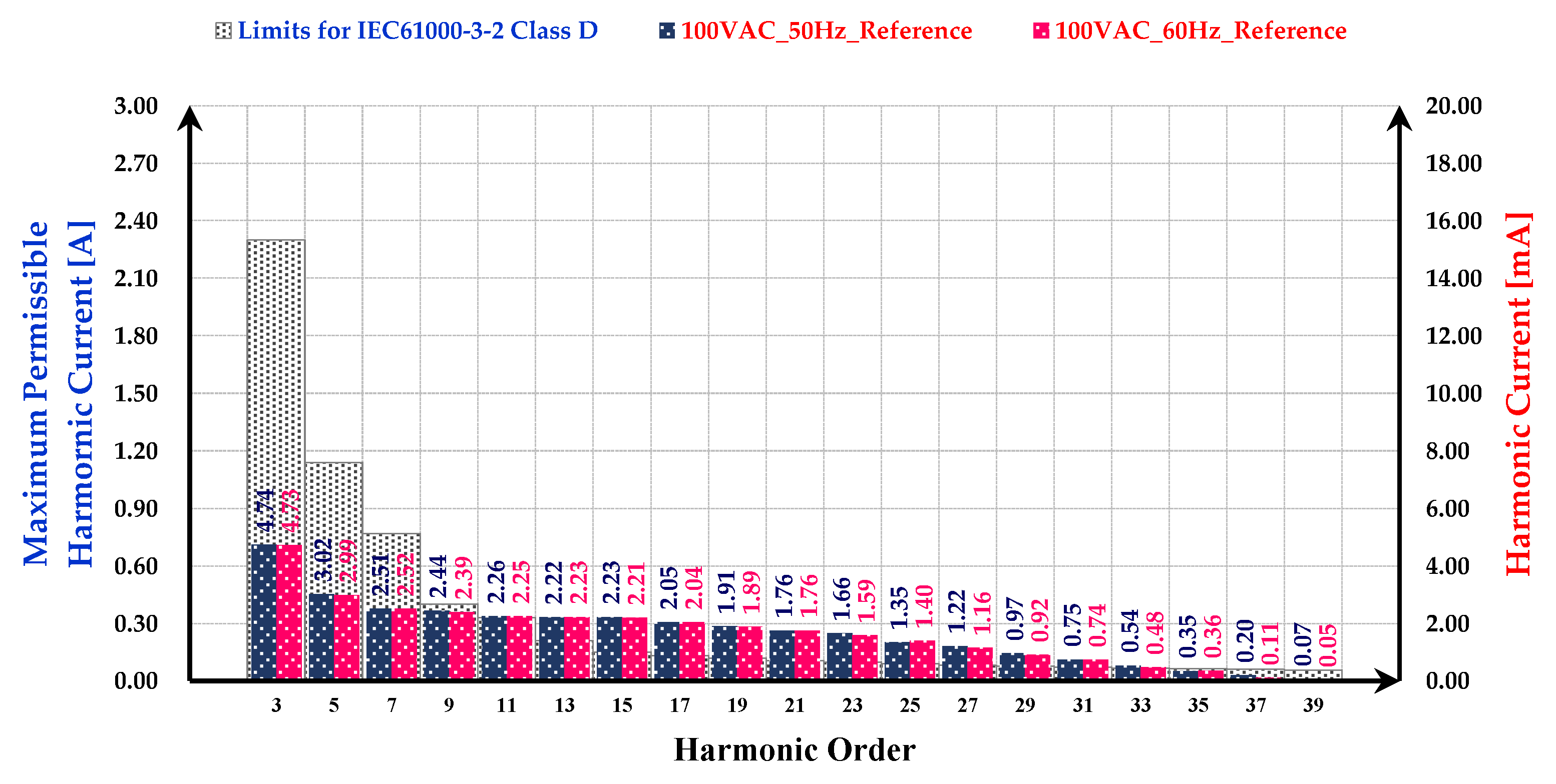
Figure 12 shows the measured results of the harmonic current at 100 VAC at 50 Hz and 60 Hz. The maximum permissible harmonic current from the IEC 61000-3-2 Class D standard for less than 25 W of lighting is presented with a gray bar [28,29]. The harmonic current is markedly lower than the IEC standards.
5. Conclusions
In this study, an AC/DC LED converter has been proposed to remove the flicker of a T8 LED tube. The proposed LED converter uses an output ripple eliminator and a SSBB converter topology for the input voltage 100–240 VAC. A 10 W prototype was designed to verify the high performance. The calculated percent was 1.9% at all input conditions. The power efficiency is lower than that of a conventional converter by 2.7% at 100–240 VAC, but it is still high (>87% and even 89% at 220 VAC). The experimental results represented the LED output current regulation as less than 0.92% at 100–240 VAC and the LED converter has a high power factor (>0.84) and low total harmonic distortion (<14.3%). Moreover, the harmonic current of the LED converter reaches the IEC 61000-3-2 Class D standard at 100 VAC and 240 VAC input voltages for high-quality LED converters.
Author Contributions
For research articles with several authors, a short paragraph specifying their individual contributions must be provided. The following statements should be used Conceptualization, S.K. and H.J.; methodology S.K. and H.J.; software, S.K.; validation, S.K. and H.J.; formal analysis S.K. and H.J.; investigation, S.K. and H.J.; resources, S.K.; data curation, S.K.; writing—original draft preparation, S.K.; writing—review and editing, S.K. and H.J.; visualization, S.K. and H.J.; supervision, H.J. All authors have read and agreed to the published version of the manuscript.
Funding
This research received no external funding.
Conflicts of Interest
The authors declare no conflict of interest.
References
- Weir, B. Driving the 21st century’s lights. IEEE Spectrum 2012, 49, 42–47. [Google Scholar] [CrossRef]
- Tsao, J.Y. Solid-state lighting: Lamps, chips, and materials for tomorrow. IEEE Circuits Devices Mag. 2004, 20, 28–37. [Google Scholar] [CrossRef]
- Lamar, D.G.; Arias, M.; Rodriguez, A.; Fernandez, A.; Hernando, M.M.; Sebastian, J. Design-oriented analysis and performance evaluation of a low-cost high-brightness LED driver based on flyback power factor corrector. IEEE Trans. Ind. Electron. 2012, 60, 2614–2626. [Google Scholar] [CrossRef]
- Wang, Y.; Alonso, J.M.; Ruan, X. A Review of LED Drivers and Related Technologies. IEEE Trans. Ind. Electron. 2017, 64, 5754–5765. [Google Scholar] [CrossRef]
- Kim, S.H.; Lee, S. A New High-Performance LED Converter With Separation of the AC and DC Driving Parts for a T8 LED Tube. IEEE Access 2019, 7, 61433–61441. [Google Scholar] [CrossRef]
- Peretto, L.; Pivello, E.; Tinarelli, R.; Emanuel, A.E. Theoretical analysis of the physiologic mechanism of luminous variation in eye-brain system. IEEE Trans. Instrum. Meas. 2007, 56, 164–170. [Google Scholar] [CrossRef]
- Wilkins, A.; Veitch, J. A Review of the Literature on Light Flicker: Ergonomics, Biological Attributes, Potential Health Effects, and Methods in Which Some LED Lighting May Introduce Flicker; IEEE Std: Piscataway, NJ, USA, 2008; pp. 1–26. [Google Scholar]
- Wilkins, A.; Veitch, J.; Lehman, B. LED lighting flicker and potential health concerns: IEEE standard PAR1789 update. In Proceedings of the 2010 IEEE Energy Conversion Congress and Exposition, Atlanta, GA, USA, 12–16 September 2010; pp. 171–178. [Google Scholar]
- IEEE Standards Association. IEEE Standards Association. IEEE Recommended Practices for Modulating Current in High-Brightness LEDs for Mitigating Health Risks to Viewers; IEEE Std.; Piscataway, NJ, USA, 2015; pp. 1–80. [Google Scholar]
- Trujillo, C.; Henao, G.; Castro, J.; Narvaez, A. Design and development of a LED Driver prototype with a Single-Stage PFC and low current harmonic distortion. IEEE Latin Am. Trans. 2017, 15, 1368–1375. [Google Scholar]
- Mark, R.S. The IESNA, Lightging Handbook-Reference and Application (vol. 1); IESNA: New York, NY, USA, 2000. [Google Scholar]
- Fang, P.; Liu, Y. Energy channeling LED driver technology to achieve flicker-free operation with true single stage power factor correction. IEEE Trans. Power Electron. 2016, 32, 3892–3907. [Google Scholar] [CrossRef]
- Reddy, U.R.; Narasimharaju, B.L. Single-stage electrolytic capacitor less non-inverting buck-boost PFC based AC–DC ripple free LED driver. IET Power Electron. 2017, 10, 38–46. [Google Scholar] [CrossRef]
- Ahn, H.; Hong, S.; Kwon, O. A Highly Accurate Current LED Lamp Driver With Removal of Low-Frequency Flicker Using Average Current Control Method. IEEE Trans. Power Electron. 2017, 33, 8741–8753. [Google Scholar] [CrossRef]
- Pereira, G.G.; Costa, M.A.D.; Alonso, J.M.; De Melo, M.F.; Barriquello, C.H. LED driver based on input current shaper without electrolytic capacitor. IEEE Trans. Ind. Electron. 2017, 64, 4520–4529. [Google Scholar] [CrossRef]
- Fang, P.; Liu, Y.; Sen, P.C. A Flicker-Free Single-Stage Offline LED Driver With High Power Factor. IEEE J. Emerg. Sel. Top. Power Electron. 2015, 3, 654–665. [Google Scholar] [CrossRef]
- Fang, P.; Sheng, B.; Webb, S.; Zhang, Y.; Liu, Y.-F. LED Driver Achieves Electrolytic Capacitor-Less and Flicker-Free Operation with an Energy Buffer Unit. IEEE Trans. Power Electron. 2019, 34, 6777–6793. [Google Scholar] [CrossRef]
- Fang, P.; Webb, S.; Chen, Y.; Liu, Y.-F.; Sen, P.C.; Sam, W. A Multiplexing Ripple Cancellation LED Driver with True Single-Stage Power Conversion and Flicker-free Operation. IEEE Trans. Power Electron. 2019, 34, 10105–10120. [Google Scholar] [CrossRef]
- International Electrotechnical Commission. IEC 60061-1: Lamp Caps and Holders Together with Gauges for the Control of Interchangeability and Safety—PART 1: LAMP CAPS; IEC: Geneva, Switzerland, 2005. [Google Scholar]
- Wang, Y.; Zhang, S.; Alonso, J.M.; Liu, X.; Xu, D. A single-Stage LED Driver With High-Performance Primary-Side-Regulated Characteristic. IEEE Trans. Circuits Syst. II Express Briefs 2018, 65, 76–80. [Google Scholar] [CrossRef]
- Lei, C. Single Stage Primary Side Regulation PFC Controller for LED Driver; Application note AN1115 for Diodes Incorporated: Plano, TX, USA, 2015. [Google Scholar]
- Adragna, C. Design Equations of High-Power-Factor Flyback Converters Based on the L6561; Application note AN1059 for STMicroelectronics: Geneva, Switzerland, 2003. [Google Scholar]
- Diodes Incorporated. Single Stage Primary Side Regulation PFC Controller for LED Driver. AP1682E Datasheet; Diodes Incorporated: Plano, TX, USA, 2014. [Google Scholar]
- Roy, R.V. Minimizing Light Flicker in LED Lighting Applications; Application note AN022 for Richtek Technology: Hsinchu, Taiwan, 2014. [Google Scholar]
- Malik, N.R. Transistor Amplifiers. In Electronic Circuits; Prentice Hall, International: London, UK, 1995; pp. 474–572. [Google Scholar]
- Seoul Semiconductor. Specification SSC-STW8Q14BE. SSC-STW8Q14BE Technical Datasheet; Seoul Semiconductor: Gyeonggi-do, Korea, 2012. [Google Scholar]
- On Semiconductor. Complementary Power Darlingtons. MJF6388 Datasheet; On Semiconductor: Pheonix, AZ, USA, 2014. [Google Scholar]
- International Electrotechnical Commission. Electromagnetic Compatibility, Part 3, Section 2. Limits for Harmonic Current Emissions (Equipment Input Current ≤ 16 A Per Phase), IEC Standard 61000-3-2; IEC: Geneva, Switzerland, 2005. [Google Scholar]
- EPSMA Technical Committee. PFC Harmonic Current Emissions—Guide to EN61000-3-2:2014; EPSMA: Little Haseley, Oxfordshire, UK, 2018. [Google Scholar]
Figure 1.
The block diagram of typical single-stage buck-boost light-emitting diode (LED) converter.
Figure 1.
The block diagram of typical single-stage buck-boost light-emitting diode (LED) converter.

Figure 2.
(a) Overall stages of the proposed LED converter; (b) simplified circuit diagram of AC and DC driving circuit.
Figure 2.
(a) Overall stages of the proposed LED converter; (b) simplified circuit diagram of AC and DC driving circuit.

Figure 3.
The output ripple eliminator.
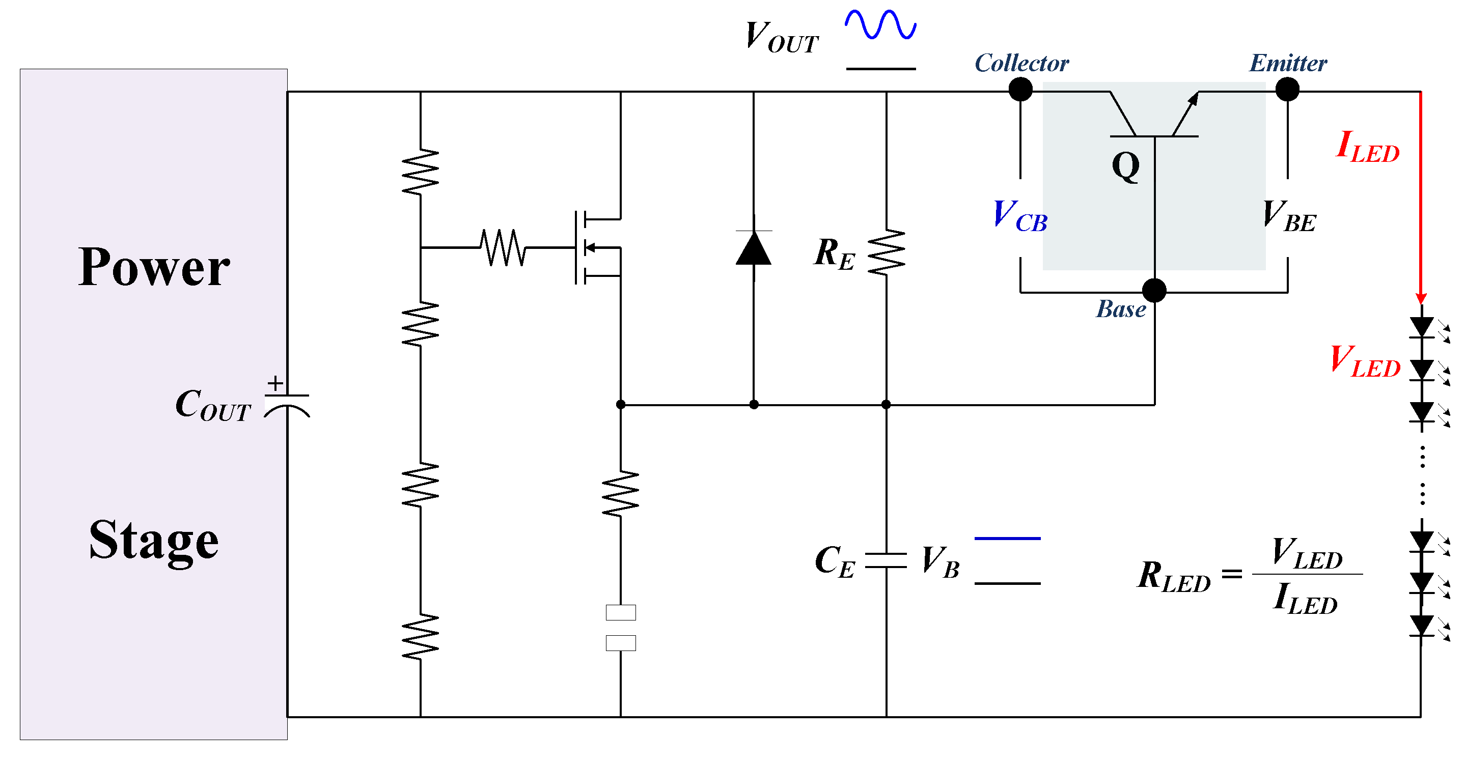
Figure 4.
Conceptual waveforms of the output ripple eliminator.
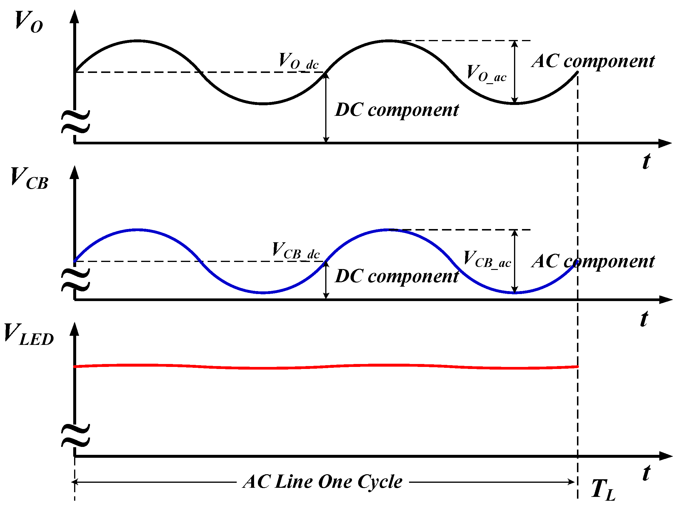
Figure 5.
(a) AC driving circuit, (b) DC driving circuit, (c) LED module with the output ripple eliminator.
Figure 5.
(a) AC driving circuit, (b) DC driving circuit, (c) LED module with the output ripple eliminator.
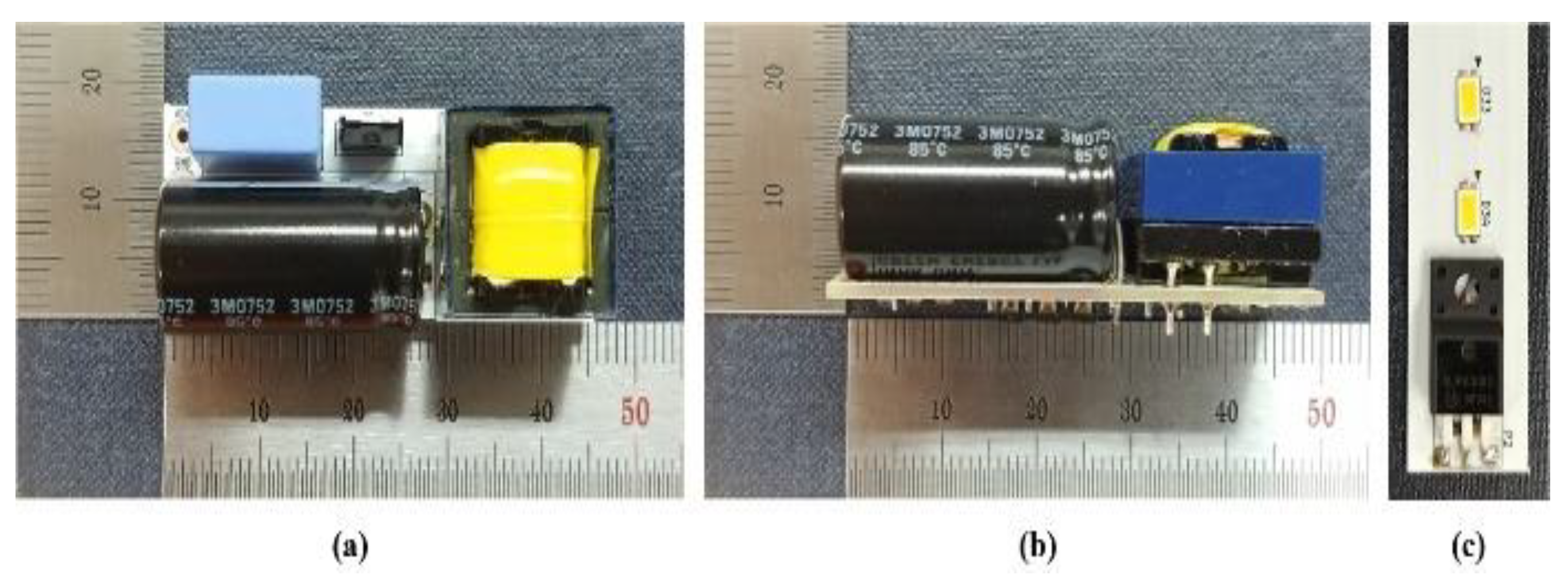
Figure 6.
Input voltage waveform (red) and input current waveform (blue) (a) at 100 VAC/60 Hz, (b) 100 VAC/50 Hz, (c) 240 VAC/50 Hz, (d) 240 VAC/50 Hz.
Figure 6.
Input voltage waveform (red) and input current waveform (blue) (a) at 100 VAC/60 Hz, (b) 100 VAC/50 Hz, (c) 240 VAC/50 Hz, (d) 240 VAC/50 Hz.
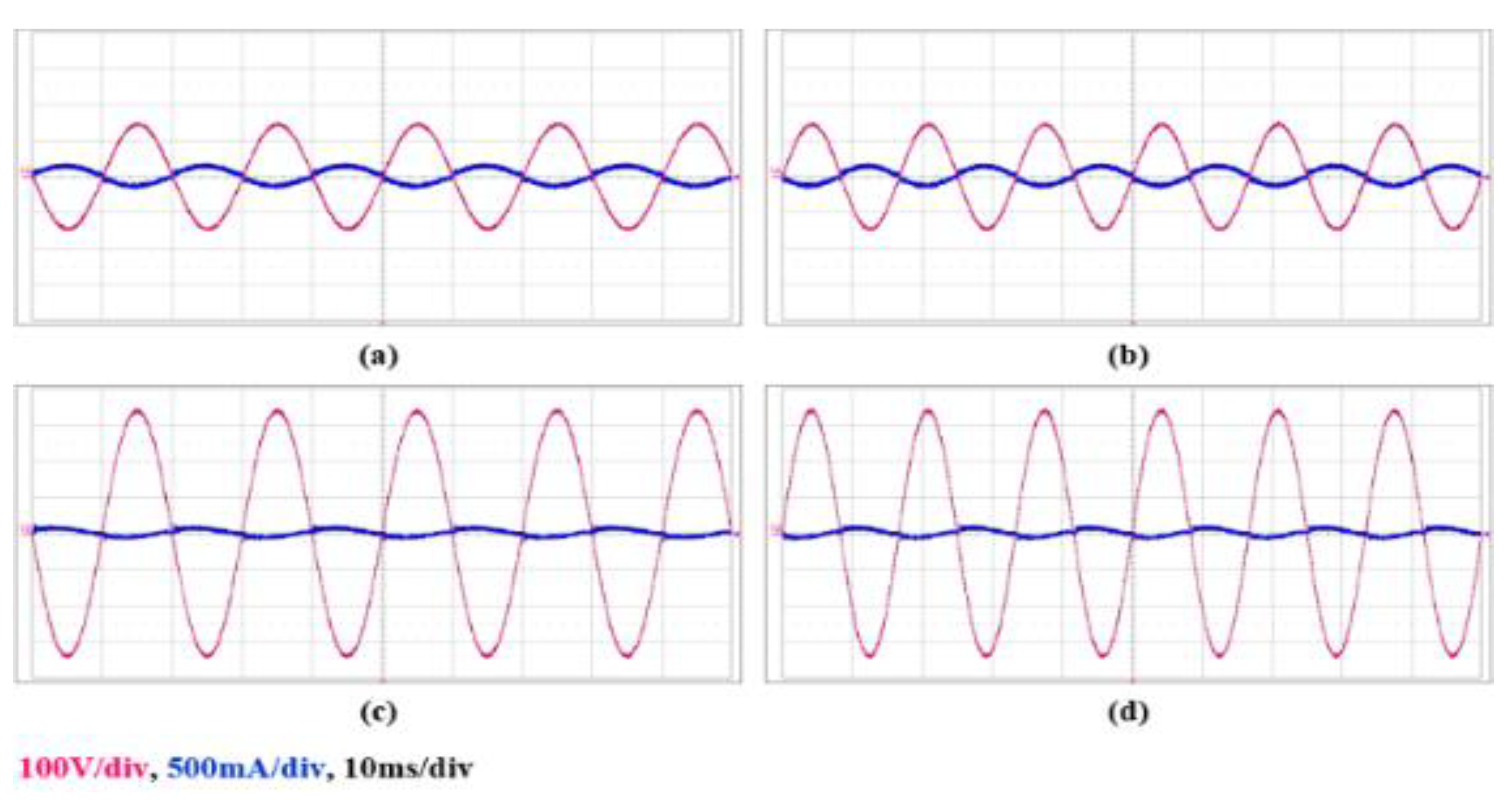
Figure 7.
Waveform of the output voltage (dark yellow), output current (blue) and light output (green) of the (a) reference converter, (b) proposed converter.
Figure 7.
Waveform of the output voltage (dark yellow), output current (blue) and light output (green) of the (a) reference converter, (b) proposed converter.
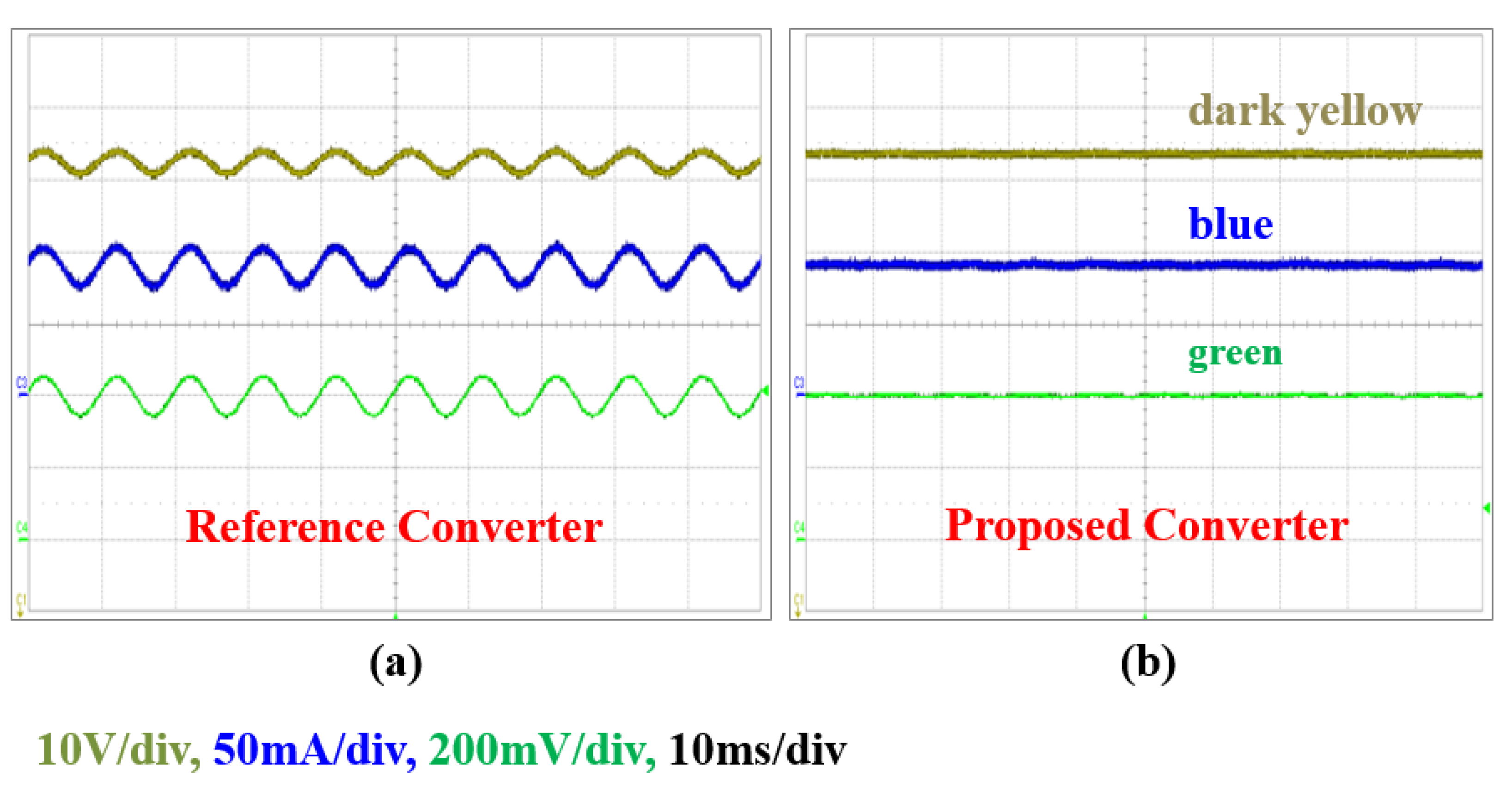
Figure 8.
Power efficiency and efficiency difference according to the input voltage.
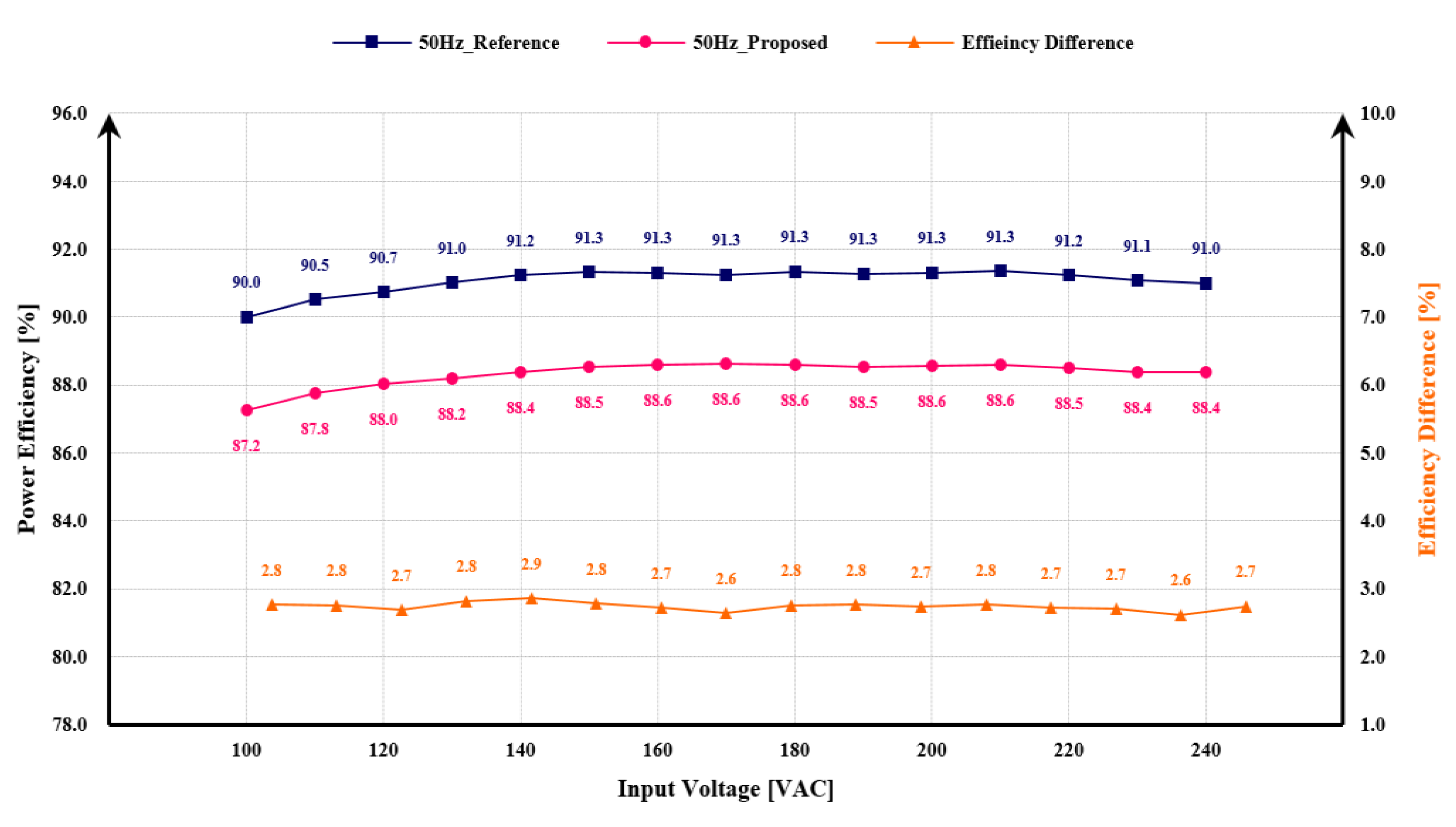
Figure 9.
Output current according to the input voltage.

Figure 10.
PF at 60 Hz.
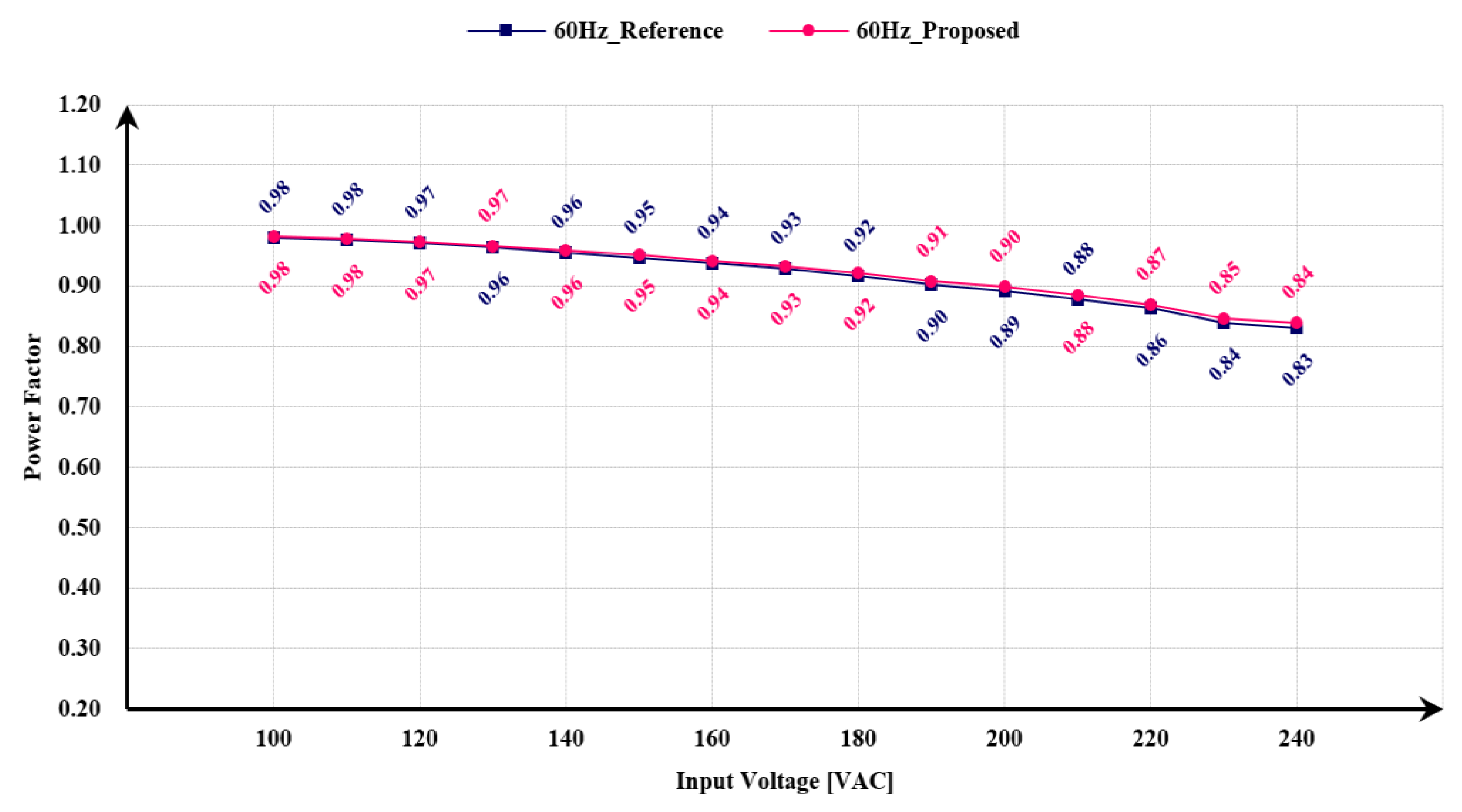
Figure 11.
Total harmonic distortion (THD) according to the input voltage.
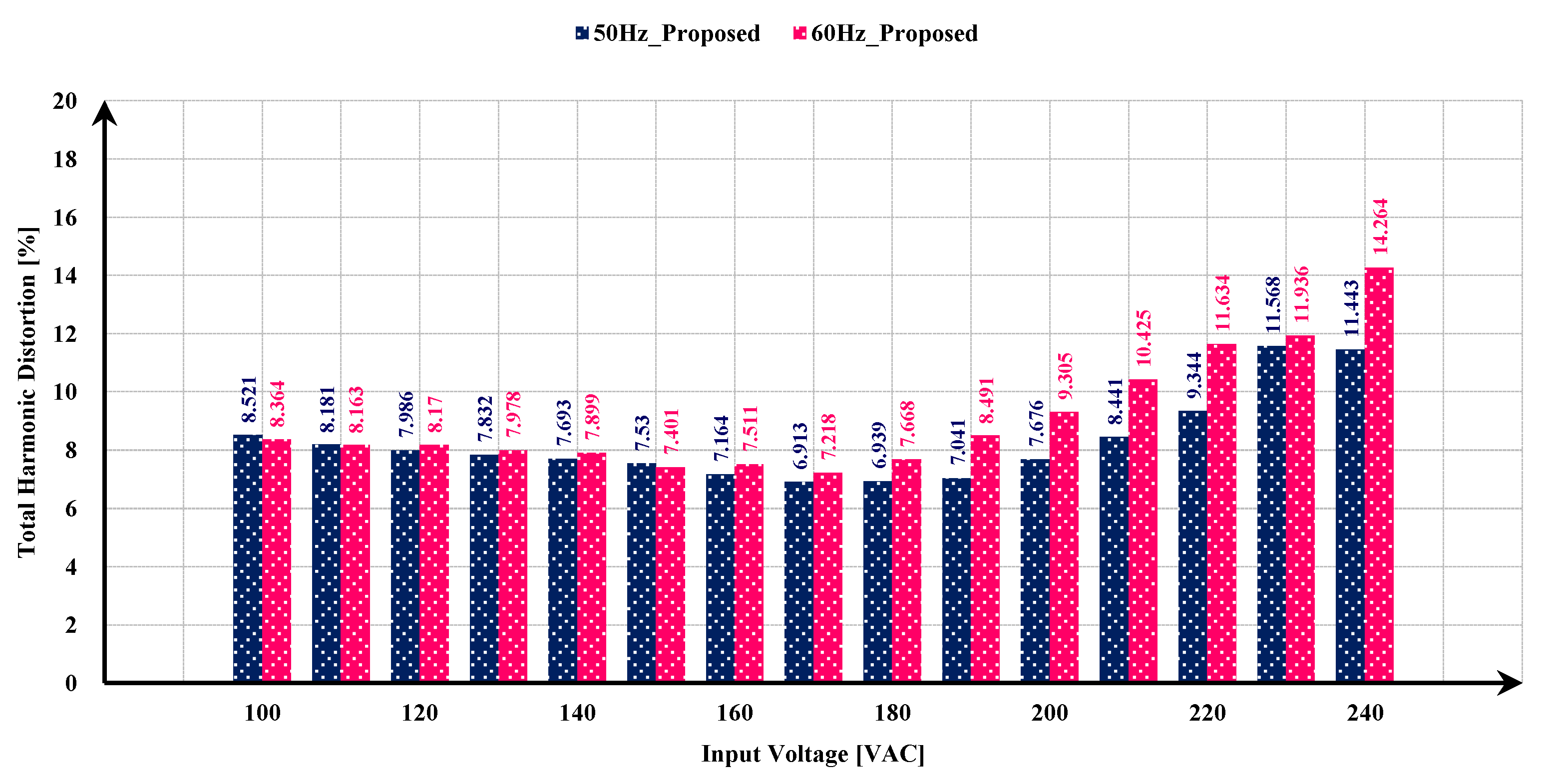
Figure 12.
Harmonic current at 100 VAC 50/60 Hz.

Table 1.
Specifications of the proposed LED converter.
| 10 W LED Converter | ||||
|---|---|---|---|---|
| Item | MIN | TYP | MAX | |
| Input Voltage (VAC) | 100 | 90 | 100 | - |
| 240 | - | 240 | 264 | |
| Input Current (mA) | 34.1 (@90 VAC) | - | 122.2 (@264 VAC) | |
| Input Frequency (Hz) | 50 | - | 60 | |
| Input Power (W) | 9.0 | 10.0 | 11.0 | |
| Output Voltage (V) | 102 | 106 | 112 | |
| Output Current (mA) | 81.8 | 87.0 | 92.2 | |
Table 2.
Specifications of key components.
| AC Driving Circuit | Fuse | 250 V, 1 A |
| Line Filter | TOROIDAL, 31 uH, 4 A | |
| X-capacitor | 275 VAC, 100 nF | |
| Bridge Diode | VRRM = 1000 V, IO = 1 A | |
| Film Capacitor | 600 V, 100 nF | |
| PCB | CEM-3, 1T, 0.5 oz, Single Layer | |
| DC Driving Circuit | Film Capacitor | 630 V, 100 nF |
| Inductor | EE1616, 1.38 mH | |
| Electrolytic Capacitor | 400 V, 22 uF, 105 °C | |
| FET | VDSS = 800 V, ID = 2.5A, RDS(ON) < 4.5 Ω | |
| Diode | VRRM = 1000 V, IO = 1 A | |
| PCB | FR-4, 1T, 0.5 oz, Double Layer | |
| Darlington Transistor | NPN, VCE 100 V, IC = 10 A |
Table 3.
Comparison of percent flicker.
| Input | Reference | Proposed | |||||||
|---|---|---|---|---|---|---|---|---|---|
| Light Output (mV) | Percent Flicker (%) | Light Output (mV) | Percent Flicker (%) | ||||||
| VAC | Hz | MAX | AVG | MIN | MAX | AVG | MIN | ||
| 100 | 50 | 450 | 393 | 336 | 14.5 | 401 | 393 | 385 | 2.0 |
| 60 | 443 | 394 | 345 | 12.5 | 402 | 395 | 388 | 1.8 | |
| 240 | 50 | 451 | 394 | 337 | 14.5 | 401 | 393 | 385 | 2.0 |
| 60 | 443 | 394 | 345 | 12.4 | 400 | 393 | 386 | 1.8 | |
Publisher’s Note: MDPI stays neutral with regard to jurisdictional claims in published maps and institutional affiliations. |
© 2021 by the authors. Licensee MDPI, Basel, Switzerland. This article is an open access article distributed under the terms and conditions of the Creative Commons Attribution (CC BY) license (http://creativecommons.org/licenses/by/4.0/).
Share and Cite
MDPI and ACS Style
Kim, S.; Jung, H. A New Circuit Design of AC/DC Converter for T8 LED Tube. Appl. Sci. 2021, 11, 421. https://doi.org/10.3390/app11010421
AMA Style
Kim S, Jung H. A New Circuit Design of AC/DC Converter for T8 LED Tube. Applied Sciences. 2021; 11(1):421. https://doi.org/10.3390/app11010421
Chicago/Turabian StyleKim, Sunghwan, and Haiyoung Jung. 2021. "A New Circuit Design of AC/DC Converter for T8 LED Tube" Applied Sciences 11, no. 1: 421. https://doi.org/10.3390/app11010421
Note that from the first issue of 2016, this journal uses article numbers instead of page numbers. See further details here.