Article

Influence of Microcracks on Silver/Polydimethylsiloxane-Based Flexible Microstrip Transmission Lines

1
College of Electronic and Optical Engineering & College of Microelectronics, Nanjing University of Posts and Telecommunications, Nanjing 210023, China
2
Warning Center, Earthquake Administration of Shanxi Province, Taiyuan 030021, China
3
National and Local Joint Engineering Laboratory of RF Integration and Micro-Assembly Technology, Nanjing University of Posts and Telecommunications, Nanjing 210023, China
*
Authors to whom correspondence should be addressed.
Appl. Sci. 2021, 11(1), 5; https://doi.org/10.3390/app11010005
Submission received: 19 November 2020 / Revised: 17 December 2020 / Accepted: 18 December 2020 / Published: 22 December 2020
(This article belongs to the Section Applied Physics General)

Abstract

:
Microcrack is commonly seen as a defect in materials that affects the performance of flexible radio frequency (RF) devices. Here, we investigate the influence of microcracks on the RF characteristics of flexible microstrip by stretching flexible microstrip that is based on polydimethylsiloxane (PDMS) substrate and an Ag microparticles/PDMS (AgMP/PDMS) composite conductor. The RF characteristics of the microstrip were monitored with a variety of tensile displacements. An equivalent circuit model of the microstrip with microcracks was proposed to reveal the mechanisms. The fitting results matched the actual measurement well. In addition, the morphology of the microcracks was characterized by SEM and the direct-current (DC) resistance was monitored. The results show that the changes in equivalent circuit element parameters (R, L, C) are due to the change in the conductive pathways, which affect the transmission and reflection of the RF signals.

1. Introduction

Recently, a variety of flexible and wearable electronic devices have appeared on the market. Particularly for the development of microwave technology, flexible radio frequency (RF) devices have attracted growing attention due to their flexibility, light weight, low power consumption and good biocompatibility, and have been applied in wireless communication [1,2,3,4,5,6,7], biomedicine [8,9,10,11], sensing [12,13] and military [14] fields. Flexible RF devices are obtained by improving the physical material or structure of traditional RF devices, so that they can possess the excellent electrical characteristics of traditional RF devices under deformation. Up to now, tremendous work has been performed on flexible materials to realize the flexibility of RF devices.
There is a considerable amount of research focused on plastic substrates. In some research, flexible RF devices are prepared by fabricating a structure made of some metal materials on flexible substrate. For example, Au/Ti was deposited on polyether sulfone (PES) substrate to fabricate a coplanar waveguide for flexible monolithic microwave integrated circuit (MMIC) [1]. A method to prepare flexible frequency selective surface (FSS) polarizer is to glue copper tapes with a designed pattern to paper substrate [14]. Gold layers patterned on polyimide film and then coated with a thick polydimethylsiloxane (PDMS) layer have been used to obtain a flexible RF reasoner in medical research [11]. In addition, novel nanomaterials such as silver nanoparticle [4,5,12], silver nanowire [5] and silicon nanomembrane [2] are also reported to be used to manufacture flexible RF devices. Li et al. fabricated flexible antenna on textile by inkjet printing technology [4]. An RF switch was developed by flip-transferring single-crystal silicon nanomembranes on plastic substrates by Qin and partners [2]. Inui et al. prepared a flexible antenna on a nanopaper mixed with silver nanowire [5]. However, microcracks may appear when the flexible RF devices suffered from larger deformations.
Microcracks, which commonly appear when structural materials are bended, stretched or suffer from other deformations, are usually considered defects [15]. For flexible electronics, microcracks may result in the degeneration of the device’s performance [16]. The negative influences are more pronounced when the flexible electronics are required to be more flexible and stretchable for some applications such as electronic skin [17], flexible display [18] and implantable devices [19]. Therefore, in terms of stretchable RF devices, the influence of microcracks on RF characteristics has to be addressed.
Herein, this paper aims to reveal the influence of microcracks on RF performance in flexible microstrip transmission lines. The microstrip, which consists of stretchable Polydimethylsiloxane (PDMS) substrate and an Ag microparticles/PDMS (AgMP/PDMS) composite strip conductor, was fabricated and stretched to form microcracks in the strip conductor. The RF characteristics of the microstrip were monitored with a variety of tensile displacements. Both the transmission and reflection characteristics can be tuned via strain. An equivalent circuit model of microstrip with microcracks was proposed to reveal the mechanisms. The calculation results show a good match with the experimental results. It was found that both the effective resistance, which contributes form resistivity change of the material and change of the conductive pathways, effective inductance and effective capacitance, which result from the microcracks, can lead to the change in RF characteristics. Additionally, further investigations were conducted to confirm this mechanism. The morphology of the microcracks was characterized by SEM and the direct-current (DC) resistance of the strip conductor was monitored under strain. This study will be helpful in the future design of flexible RF devices.

2. Design, Fabrication and Characterization

2.1. Microstrip Design

A microstrip is a strip transmission line separated from the ground plane by a substrate. Some RF components such as filter, power divider and antenna can be designed based on a microstrip. PDMS has the advantages of a high dielectric constant, good mechanical property and relative low dielectric loss [20]. Herein, a flexible microstrip with PDMS substrate and a strip conductor made of AgMP/PDMS composite was designed. The conductivity, σ, of the strip conductor was 3.33 × 10⁵ S/m, which was calculated from σ = L R W T s , where R, L, W and Ts are the resistance, length, width and thickness of the strip conductor, respectively. The resistance, R, was measured by a digital multimeter (UT71B, Uni-Trend Technology Inc.China). The structure is shown in Figure 1a. In order to match 50 Ω system impedance, the geometric parameters of the microstrip were calculated and are listed in Table 1.

2.2. Fabrication Process

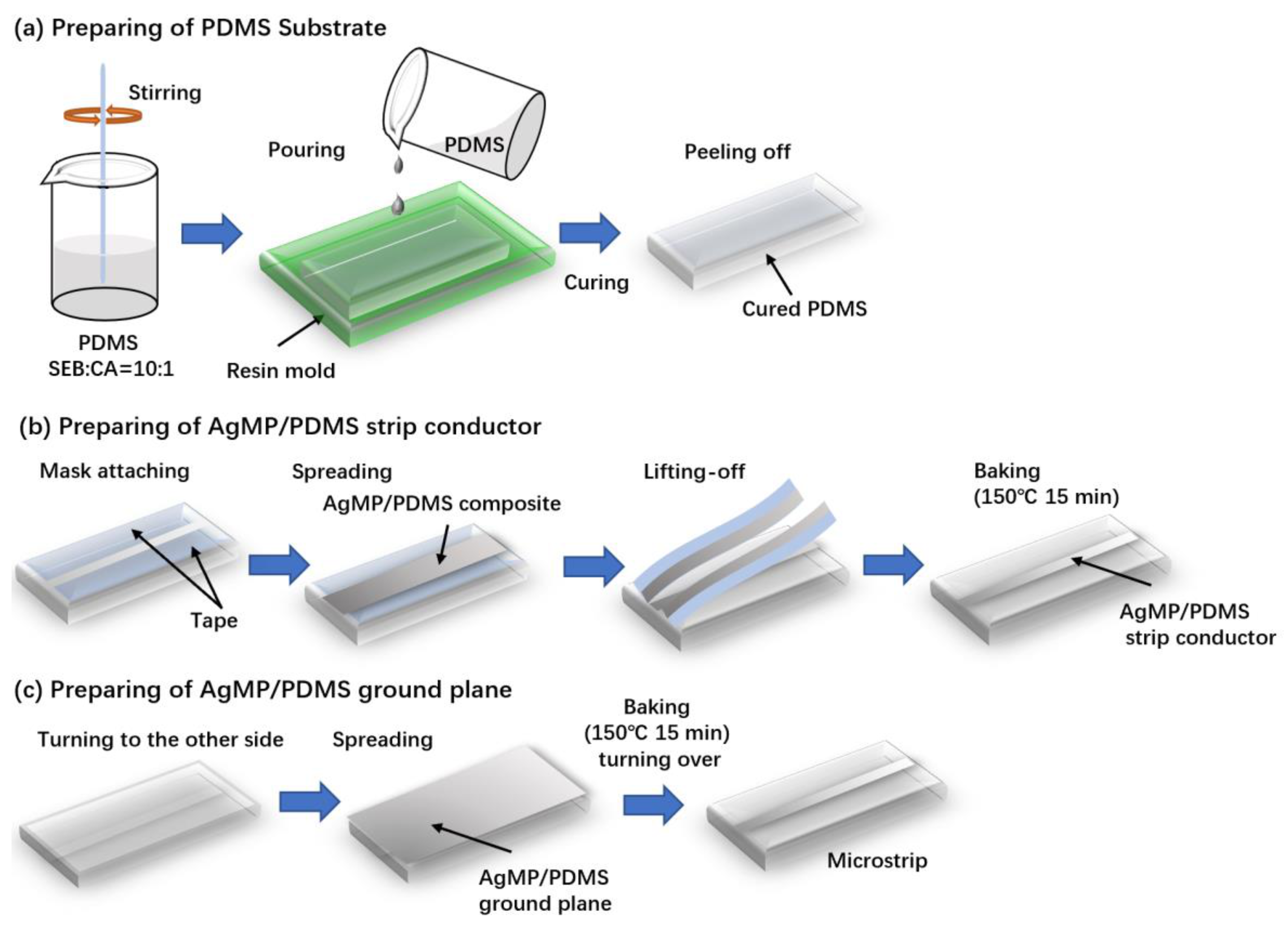
The fabrication of the microstrip is shown in Figure 2. The substrate of the microstrip is based on a commercial silicone elastomer, PDMS (Sylgard 184, Dow Corning, Inc., Midland, MI, USA). Firstly, the silicone elastomer base (SEA) and curing agent (CA) were mixed with a weight ratio of 10:1, followed by a 15-min stirring and vacuum degassing process. The mixture was poured into a resin mold with a groove (60 × 15 × 1 mm3), cured at 80 °C and peeled off from the resin mold. The strip conductor was fabricated based on a tape-assisted lift-off process. The mask for the lift-off procedure was prepared by attaching invisible matte-finish tapes (Scotch Magic, 3M Company, Saint Paul, MN, USA) onto the PDMS substrate surface. A rectangular area (50 × 2.7 mm2) was left blank for the strip conductor. The conductive AgMP/PDMS composite was prepared by mixing silver microparticle powder of 2 μm in diameter (2 μm AR grade, Nangong Xindun Alloys Spraying Co., Ltd., Beijing, China) and the same uncured PDMS mixture in a weight ratio of 9:1 with vast stirring. Then the AgMP/PDMS composite was spread onto the PDMS film surface by a glass stirrer of 7 mm in diameter. After it was peeled off the mask, the sample was baked on a hot plate at 150 °C for 15 min. Then, the sample was turned over to fabricate the ground plane. The AgMP/PDMS composite was spread and cured with the same procedure as the strip conductor.

2.3. Characterization

Two sub-miniature-A (SMA) connectors were connected to the ends of the strip conductor to obtain a solid connection with the silver paste, as shown in Figure 1b. The microstrip was stretched by a program-controlled moving platform. A vector network analyzer (Keysight E5071C) with typical 50 Ω port resistance was used to record the RF characteristics of the microstrip under a strain from 1 GHz to 18 GHz. Short-open-load-thru (SOLT) calibrations were conducted to reduce the error before measuring the RF characteristics [21]. The DC resistance was measured by a digital source meter (2400, Keithley Instruments, Cleveland, United States). The morphology and microstructures of microcracks were characterized by a scanning electron microscope (SEM, ZEISS GeminiSEM 500).

3. Results and Discussions

3.1. The Equivalent Circuit Model of the Microstrip with Microcracks

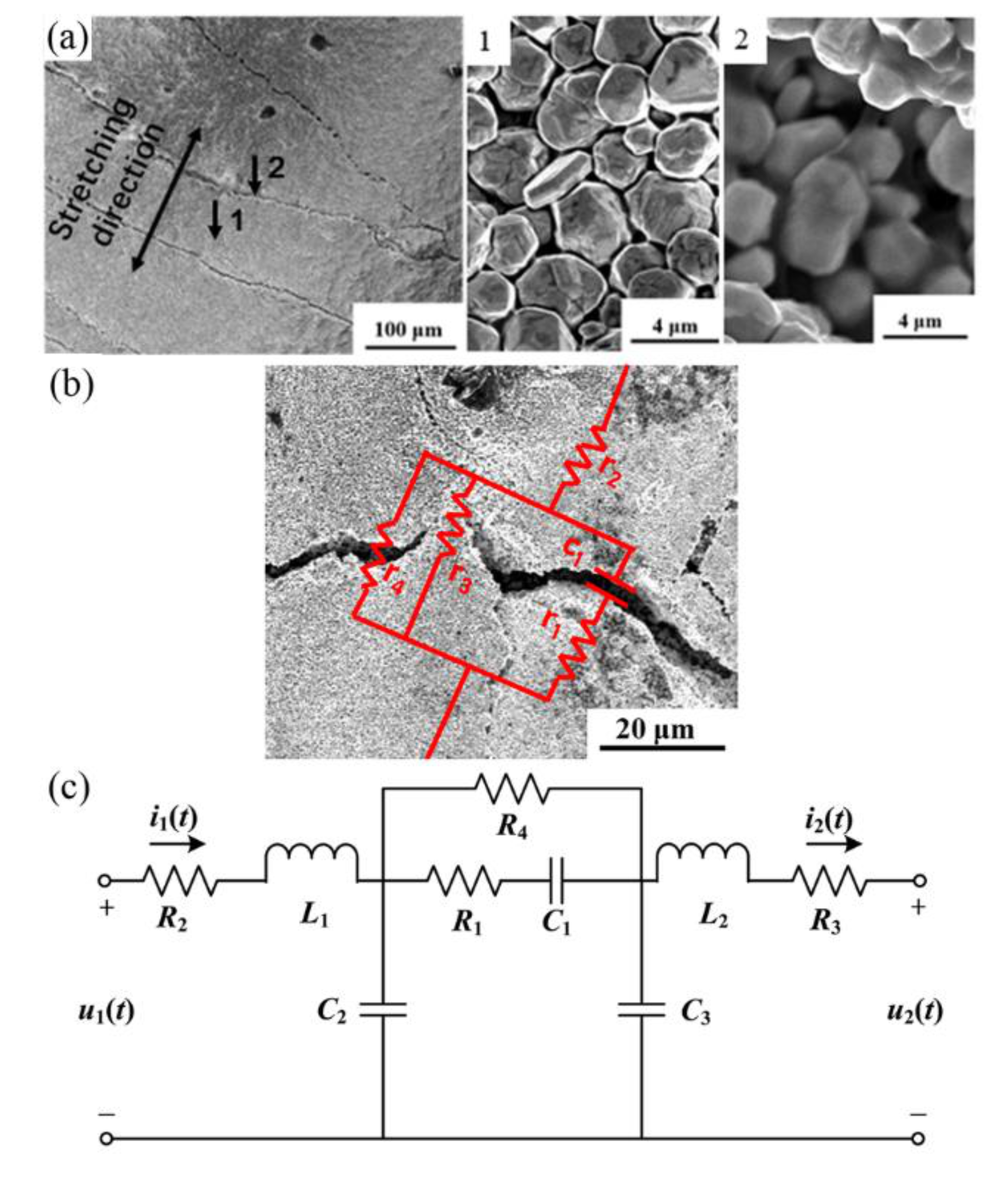
To illustrate the microcracks, Figure 3a exhibits SEM images of the fracture surfaces of the strip conductor of the microstrip. After a prestretch process, the microcracks are approximately perpendicularly oriented with respect to the strain. The microcracks illustrated moderate wavy shapes at a higher magnification as shown in Figure 3b. The microcrack was about 4 μm in width with random-distributed finer microcracks of less than 0.6 μm in width. We noted that the microcrack was discontinued where the AgMP/PDMS was partially bridge-connected across the microcracks, leading to some conductive paths. Similarly, the AgMP/PDMS thin film was also connected at the bottom of the microcrack. This may be attributed to the nonuniform strain distribution in the composite film. Upon stress, the strain first locates in the interfaces between the silver particles and PDMS, and then cracks nonuniformly originate and propagate in the AgMP/PDMS layer, possibly due to the tractive effort of the localized stress on the interface [22].
To reveal the influence of the microcrack on RF characteristics, we proposed an RF local equivalent circuit model in accordance with the micromorphology of an identical microcrack on the AgMP/PDMS composite strip conductor, as the red lines demonstrate in Figure 3b. The microcrack with a valley-liked shape involved an insulated air gap with two conductive AgMP/PDMS scarps on both sides. This configuration can be equivalent to a microcapacitor and is marked as c1. The resistors r3 and r4 represent the resistance where the microcrack was bridge-connected across the valley or at the bottom of the film, respectively. Considering the nonzero resistivity of the AgMP/PDMS composite film, two resistors r1 and r2 were also induced to the equivalent circuit to reflect the RF losses.
From a device perspective, we proposed a π equivalent circuit for the whole microstrip with microcracks, which can be seen as adding the series of the local equivalent circuits to the standard RF equivalent circuit for a microstrip transmission line as stretched in Figure 3c. The equivalent-circuit elements were deduced from the local elements, which are marked in Figure 3b. The presence of resistances R1, R2, R3 and R4 were attributed to the finite conductivity of the conductor, which leads to the conductor losses and the reflection of the RF signal [23]. The resistance R4, related to the resistance r3 and r4 in Figure 3b, represented the equivalent resistance across the microcrack. The series inductances L1 and L2 represented the self-inductance of the conductor. The capacitance C1 was derived from the microcrack, and C2, and C3 were the equivalent capacitances between the conductor and ground plane for a standard microstrip transmission line.

3.2. RF Characteristics of the Microstrips under Strain

To explore the RF characteristics of the microstrips under strain, S-parameters were monitored upon strain. S11 spectra, which represented the reflection of the RF signals, are shown in Figure 4a. When the strain was lower than 5%, the S11 values were typically bellow −16 dB at an RF frequency lower than 8 GHz and below −10 dB at frequencies from 8 GHz to 18 GHz. This indicated that the RF signals pass through the microstrip with low reflections. With the increase of strain from 5% to 10%, S11 values gradually increased to approximately −5 dB at a frequency below 8 GHz, showing a significant increase of the reflections. However, the S11 values kept stable at higher frequencies, which indicate the strain mainly affects the reflections of RF signals at a lower frequency range; below 8 GHz in our case.
The S21 parameter reflecting the transmission characteristics of the microstrips is plotted in Figure 4b. Upon strain, the S21 values dramatically decrease with an increasing strain. When the strain increased to 5%, the S21 values showed a slight, approximately 3 dB, decrease. However, when the strain increased from 5% to 10%, a significant drop in S21 values was observed. The minimum S21 value even went below −35 dB for a transmission line upon 10% strain. We noted that upon a certain strain, the S21 values decreased gradually with the increase of frequency. Also, a larger strain leads to a sharper drop of the S21 value over the frequency. Overall, the transmission of a microstrip shows inverse correlations with the strain.
To give an insight into the RF characteristics upon strain, fittings were conducted from 1 GHz to 18 GHz according to the equivalent circuit stretched in Figure 3c and the measured S-parameters plotted in Figure 4. The fitting results are plotted in Figure 5 with a good match of the data in Figure 4. Silver paste was used for the connection between SMA connectors and the microstrip, which caused impedance discontinuity and led to the differences in fitting and measurement results. The element parameters used for the fittings are listed in Table 2. For convenience, ΔR1, ΔR2, ΔR3, ΔR4, ΔL1, ΔL2 and ΔC1 were induced to mark the changes of R1, R2, R3, R4, L1, L2 and C1 respectively, when the microstrip was stretched.

3.3. Analysis and Discussions of the Element Parameters

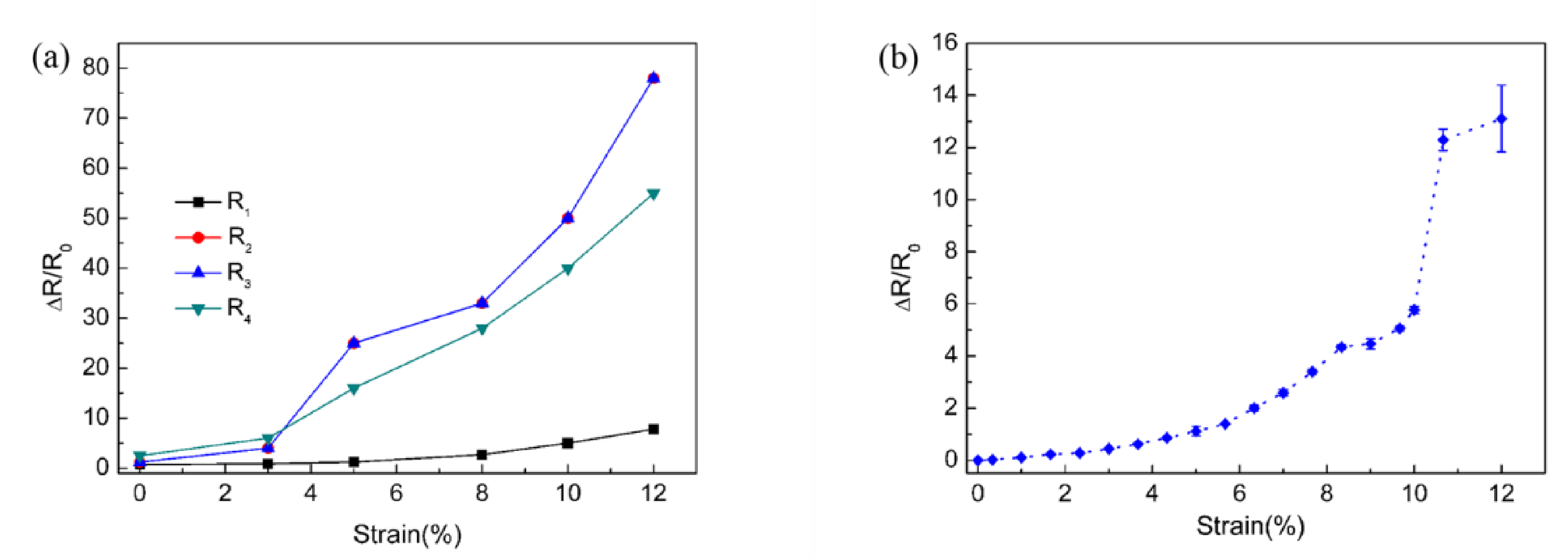
To provide deeper insight into the influence of the strain on the element parameters of the equivalent circuit model, we plotted the element parameter values as functions of the strain. The resistances R1, R2, R3 and R4 increased with the strain as illustrated in Figure 6a. This can be mainly attributed to two factors. First, the formation and extension of microcracks leads to the breakdown of the conductive pathways. Second, the elongation of the AgMP/PDMS composite leads to an increase of the resistivity of the composite. This is because the distance between AgMP fillers become bigger during the stretching, leading to damage of the conductive networks [24]. These two mechanisms can be revealed by the DC resistance of the strip conductor. Here, a digital multimeter (UT71B, Uni-Trend Technology Inc., Beijing, China) was used to monitor the real-time DC resistance of the strip conductor. The relative resistance change (ΔR/R0) under strain was shown in Figure 6b. It rose slowly with a relatively low strain (Δε ≤ 5%), and then increased rapidly with higher strains (Δε ≥ 5%). This was consistent with the RF equivalent resistance with an increasing strain (Figure 6a).
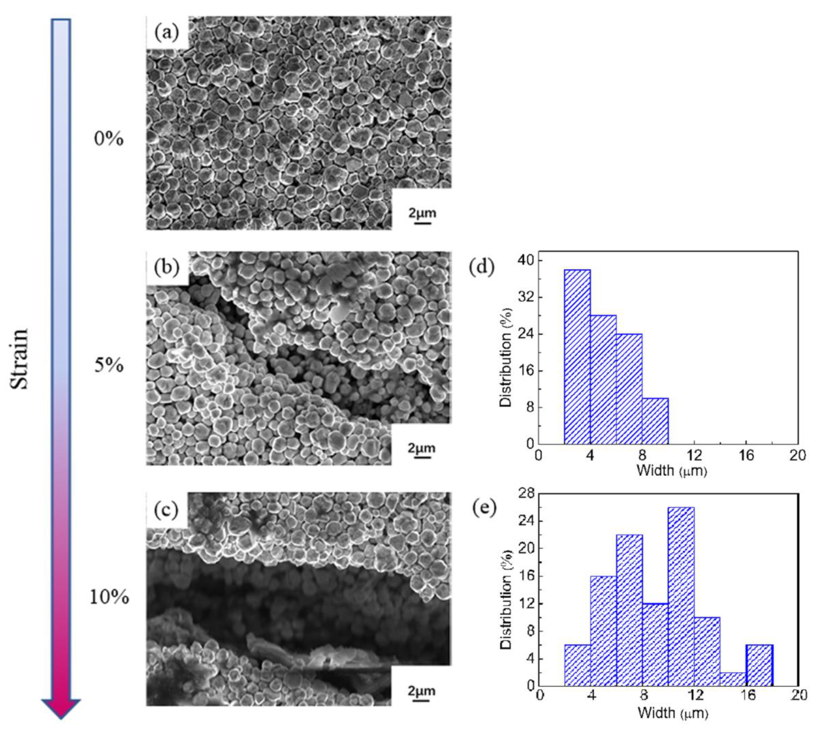
An additional experiment was conducted by SEM observation of the microcracks under strain as shown in Figure 7. Initially, the strip conductor layer was continuous with the silver micro-particles uniformly distributed in the PDMS and no crack was found as shown in Figure 7a. When the conductor was stretched, the microcracks generated on the surface of the AgMP/PDMS film, whereas the AgMP/PDMS film was still connected around the interface between the AgMP/PDMS film and PDMS substrate as shown in Figure 7b. Further increasing the strain from 5% to 10% broadened and deepened the crack as Figure 7c shows. The width distributions of microcracks are shown in Figure 7d,e corresponding to 5% and 10% strain, respectively. The average width of the microcracks was about 5 μm under 5% strain, and approximately 9 μm under 10% strain. We could observe that the size of the microcrack increased with the increase of strain. The expansion of the microcrack at a higher strain will certainly result in the reduction of the conductive pathways and the increase of both the RF equivalent resistances and DC resistance, which is consistent with the observations in Figure 6.
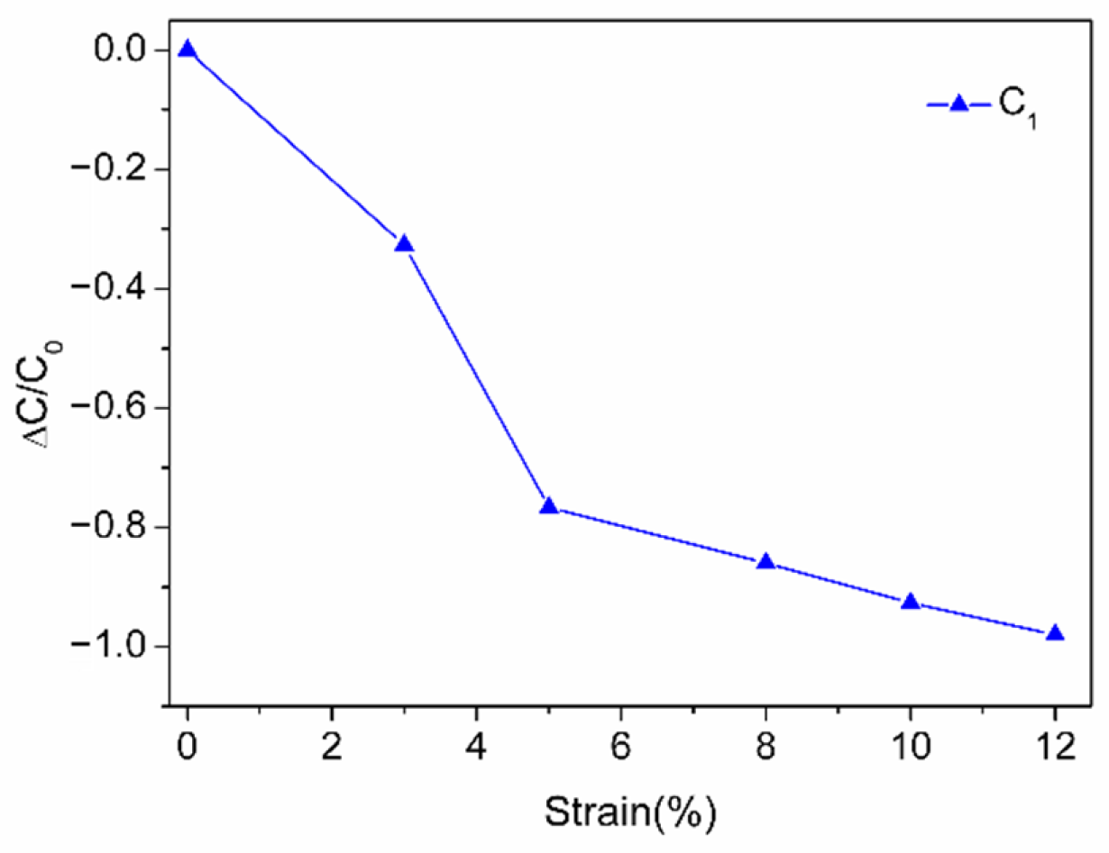
The RF equivalent capacitances C1 are plotted in Figure 8. The capacitance C1 related to the microcracks decreased with the increasing strain as shown in Figure 8. This can be attributed to the enlargement of the crack width as shown in Figure 7. The capacitance can be delivered from the formula C = ε S d [25], where ε is the dielectric constant of PDMS, S is the cross-sectional area of the microcrack in AgMP/PDMS conductor and d is the width of the microcrack. Thus, the increase of the crack width d will result in a decrease of the equivalent capacitance.
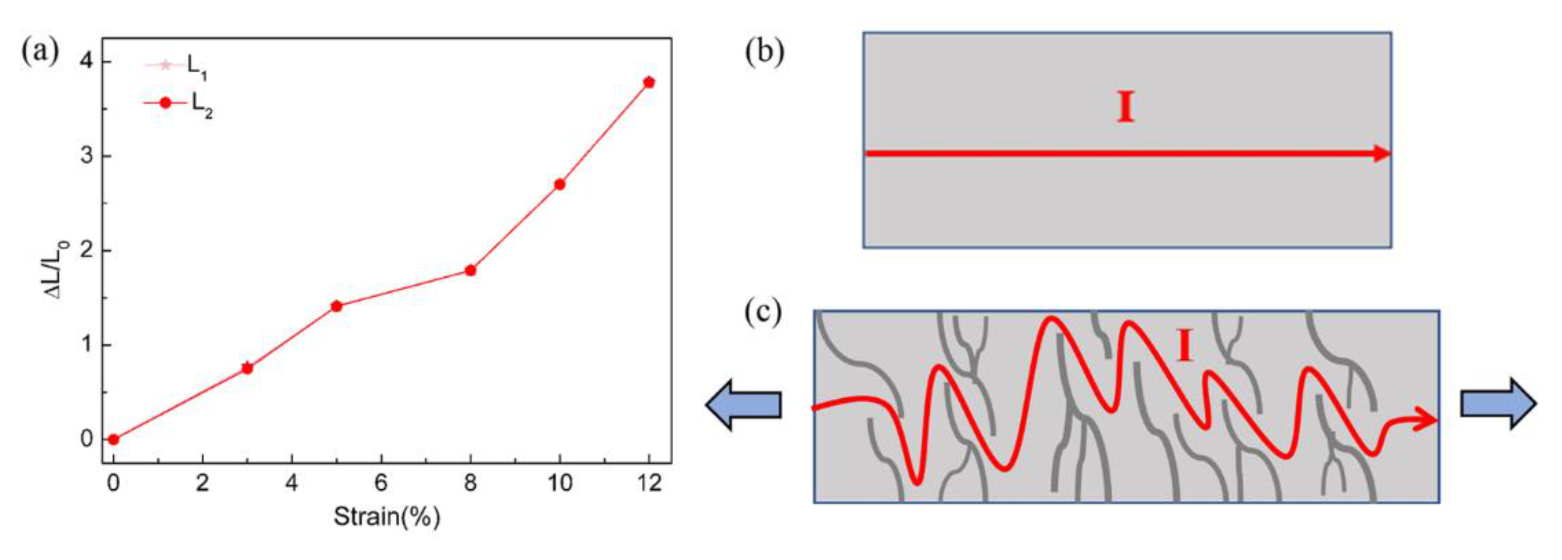
The RF equivalent inductances L1 and L2 were plotted in Figure 9a. The capacitance increased with the increasing strain. With 0% strain, the current directly flowed through the strip conductor as shown in Figure 9b. Once the microcracks formed upon strain, the microcracks will partially block the current and disturb the current distributions as illustrated in Figure 9c. This will increase the equivalent electric length and enlarge the equivalent inductance.
Generally, the drift of the element parameters in the equivalent circuit model will lead to a change of both the reflection and transmission characteristics of the transmission line. The characteristic impedance Z0 of a short section of the transmission line is calculated by Z 0 = R + j ω L G + j ω C [26], where R, G, L and C are the series resistance, parallel conductance, series inductance and parallel capacitance, respectively, and ω is the angular frequency of RF signal. Then the reflection coefficient Γ is calculated by Γ = Z L Z 0 Z L + Z 0 [26], where ZL is the load impedance. The characteristic impedance for our microstrip was matched to 50 Ω, leading to a relatively low reflection. When the microstrip is stretched, the formation and propagation of the microcracks leads to the increase of R and L, and a decrease of G and C. This will increase the characteristic impedance Z0, resulting in an impedance mismatch. Thus, the reflection coefficient will certainly increase, which leads to an increase of S11. The S21 implies the total signal eliminating the reflection loss and Ohm loss, and decreases accordingly.

4. Conclusions

In summary, the influence of microcracks on RF performance in flexible microstrip transmission lines was investigated by stretching flexible microstrip based on AgMP/PDMS conductors and PDMS substrates. The RF characteristics of the microstrips were monitored and fitted via a new proposed equivalent circuit model of a microstrip with microcracks. We found that the formation and propagation of the microcracks led to the breakdown of conductive pathways, an increase of the crack width and an increase of the equivalent electric length, and thereby result in the drift of the element parameters, i.e., effective resistance, inductance and capacitance. In all, the impendence mismatch leads to the change of both the transmission and reflection characteristics of the microstrip. This study will be beneficial for the future design of flexible RF devices.

Author Contributions

D.D., R.L. and Y.Y. conceived and designed the experiments; D.D. and R.L. performed the experiments; D.D., R.L. and J.Y. performed the simulations; D.D. and J.Y. analyzed the data; and J.L. and Y.F. contributed materials. D.D. and R.L. wrote the manuscript. All authors have read and agreed to the published version of the manuscript.

Funding

This research was funded by the National Natural Science Foundation of China (61704090, 11904177), the Natural Science Foundation of Jiangsu Province (BK20170903, BK20170908), the Natural Science Foundation of the Higher Education Institutions of Jiangsu Province (17KJA470005), and NUPTSF (NY217124).

Conflicts of Interest

The authors declare no conflict of interest.

References

  1. Yun, Y.; Kim, H.S.; Jang, N. Study on Characteristics of Various RF Transmission Line Structures on PES Substrate for Application to Flexible MMIC. ETRI J. 2014, 36, 106–115. [Google Scholar] [CrossRef]
  2. Qin, G.-X.; Yuan, H.-C.; Celler, G.K.; Ma, J.G.; Ma, Z.Q. RF model of flexible microwave switches employing single-crystal silicon nanomembranes on a plastic substrate. Microelectron. Eng. 2012, 95, 21–25. [Google Scholar] [CrossRef]
  3. Huang, C.-U.; Chen, I.-Y.; Henry, J.H.; Christina, F.J.; Huang, R.-S. 2.4 and 5.2 GHz Dual-Band Antenna Fabricated on Flexible Parylene Membrane. Jpn. J. Appl. Phys. 2005, 44, 8356–8361. [Google Scholar] [CrossRef]
  4. Li, Y.; Torah, R.; Steve, B.; Turdor, J. Inkjet printed flexible antenna on textile for wearable applications. In Proceedings of the 2012 Textile Institute World Conference, Shah Alam Selangor, Malaysia, 15–17 May 2012. [Google Scholar]
  5. Inui, T.; Koga, H.; Nogi, M.; Komoda, N.; Suganuma, K. A Miniaturized Flexible Antenna Printed on a High Dielectric Constant Nanopaper Composite. Adv. Mater. 2014, 27, 1112–1116. [Google Scholar] [CrossRef] [PubMed]
  6. Glavin, N.R.; Chabak, K.D.; Heller, E.R.; Moore, E.A.; Prusnick, T.A.; Maruyama, B.; Walker, D.E.; Dorsey, D.L.; Paduano, Q.; Snure, M. Flexible gallium nitride: Flexible gallium nitride for high-performance, strainable radio-frequency devices. Adv. Mater. 2017, 47, 1701838. [Google Scholar] [CrossRef] [PubMed]
  7. Fan, C.-Y.; Wei, M.-D.; Gjurovski, P.; Saeed, M.; Hamed, A.; Negra, R. Concept for a 16-QAM RF Transmitter on Flexible Substrate using a Graphene Technology. In Proceedings of the 2019 26th IEEE International Conference on Electronics, Circuits and Systems (ICECS), Genoa, Italy, 27–29 November 2019. [Google Scholar]
  8. Scarpello, M.L.; Kurup, D.; Rogier, H.; Ginste, D.V.; Axisa, F.; Vanfleteren, J.; Joseph, W.; Martens, L.; Vermeeren, G. Design of an implantable slot dipole conformal flexible antenna for biomedical applications. IEEE Trans. Antennas Propag. 2011, 59, 3556–3564. [Google Scholar] [CrossRef] [Green Version]
  9. Zhang, Y.; Sun, S.; Pratap, R.; Galstyan, E.; Wosik, J.; Selvamanickam, V. Development of rebco tapes on nonmetallic flexible substrates for rf applications. IEEE Trans. Appl. Supercond. 2019, 335, 3500405. [Google Scholar] [CrossRef]
  10. Tiwari, N.K.; Singh, S.P.; Mondal, D.; Jaleel Akhtar, M. Flexible biomedical RF sensors to quantify the purity of medical grade glycerol and glucose concentrations. Int. J. Microw. Wirel. Technol. 2019, 12, 120–130. [Google Scholar] [CrossRef]
  11. Alipour, A.; Gokyar, S.; Algin, O.; Atalar, E.; Demir, H.V. An Inductively Coupled Ultra-Thin, Flexible, and Passive RF Resonator for MRI Marking and Guiding Purposes:Clinical Feasibility. Magn. Reson. Med. 2018, 80, 3613–3670. [Google Scholar] [CrossRef]
  12. Rai, T.; Dantes, P.; Bahrevni, B.; Kim, W.S. A Stretchable RF Antenna with Silver Nanowires. IEEE Electron Device Lett. 2013, 34, 544–546. [Google Scholar] [CrossRef]
  13. Eom, S.-H.; Lim, S. RF Stretchable Sensor Using Flexible Substrate and Eutectic Gallium-Indium. In Proceedings of the ISAP2016, International Symposium on Antennas & Propagation, Okinawa, Japan, 24–28 October 2016. [Google Scholar]
  14. Sivasamy, R.; Kanagasabai, M. Design and fabrication of flexible FSS polarizer. Int. J. RF Microw. Comput. Aided Eng. 2020, 30, 22002. [Google Scholar] [CrossRef]
  15. Nemat-Nasser, S.; Obata, M. A microcrack model of dilatancy in brittle materials. J. Appl. Mech. 1988, 55, 24–35. [Google Scholar] [CrossRef]
  16. Guo, Y.; Guo, Z.-Y.; Zhong, M.-J.; Wan, P.-B.; Zhang, W.-X.; Zhang, L.-Q. A Flexible Wearable Pressure Sensor with Bioinspired Microcrack and Interlocking for Full-Range Human–Machine Interfacing. Small 2018, 14, 1803018. [Google Scholar] [CrossRef] [PubMed]
  17. Wang, J.; Lou, H.-Y.; Meng, J.-J.; Peng, Z.-Q.; Wang, B.; Wan, J.-M. Stretchable Energy Storage E-skin Supercapacitors and Body Movement Sensors. Sens. Actuators B Chem. 2019, 305, 127529. [Google Scholar] [CrossRef]
  18. Lee, J.K.; Kim, S.S.; Park, Y.I.; Kim, C.D.; Hwang, Y.K. In-cell adaptive touch technology for a flexible e-paper display. Solid State Electron. 2011, 56, 159–162. [Google Scholar] [CrossRef]
  19. Gibney, E. The inside story on wearable electronics. Nature 2015, 56, 26–28. [Google Scholar] [CrossRef]
  20. Lei, K.F.; Lee, K.F.; Lee, M.Y. Development of a flexible PDMS capacitive pressure sensor for plantar pressure measurement. Microelectron. Eng. 2012, 99, 1–5. [Google Scholar] [CrossRef]
  21. Zou, S.-M.; Yelamanchili, B.; Gupta, V.; Sellers, J.A.; Isaacs-smith, T.; Tuckerman, D.B.; Hamilton, M.C. Low-loss cable-to-cable parallel connection method for thin-film superconducting flexible microwave transmission lines. Supercond. Sci. Technol. 2019, 32, 1361–1373. [Google Scholar] [CrossRef]
  22. Chen, S.; Wei, Y.; Wei, S.-M.; Lin, Y.; Liu, L. Ultrasensitive Cracking-assisted Strain Sensors Based on Silver Nanowires/Graphene Hybrid Particles. ACS Appl. Mater. Int. 2016, 8, 25563–25570. [Google Scholar] [CrossRef]
  23. Li, R.-Z.; Yan, J.; Fang, Y.-M.; Fan, X.-Y.; Sheng, L.-K.; Ding, D.-Y.; Yin, X.-X.; Yu, Y. Laser-Scribed Lossy Microstrip Lines for Radio Frequency Applications. Appl. Sci. 2019, 9, 415. [Google Scholar] [CrossRef] [Green Version]
  24. Xu, C.-C.; Hu, S.-F.; Zhang, R.; Hu, H.-L.; Ying, C.; Zhang, F.; Liu, Q.-T.; Fu, X.-D. Preparation and properties of fexible conductive polydimethylsiloxane composites containing hybrid fllers. Polym. Bull. 2019, 76, 6487–6501. [Google Scholar] [CrossRef]
  25. Li, R.-Z.; Hu, A.-M.; Zhang, T.; Oakes., K.-D. Direct Writing on Paper of Foldable Capacitive Touch Pads with Silver Nanowire Inks. ACS Appl. Mater. Inter. 2014, 6, 21721–21729. [Google Scholar] [CrossRef] [PubMed]
  26. Pozar, D.M. Microwave Engineering, 3rd ed.; John Wiley& Sons: New York, NY, USA, 2010; pp. 446–448. [Google Scholar]
Figure 1. (a) The structure of the microstrip line, and (b) e photograph of a microstrip sample with sub-miniature-A (SMA) connectors, and the ground plane is on the other side of the transparent polydimethylsiloxane (PDMS) film.
Applsci 11 00005 g001
Figure 2. The fabrication process of the proposed microstrip. Preparing of (a) PDMS substrate, (b) Ag microparticles/PDMS (AgMP/PDMS) strip conductor, (c) AgMP/PDMS ground plane.
Applsci 11 00005 g002
Figure 3. (a) Scanning electron microscope (SEM) images of the microstrip with microcracks. 1 and 2 are SEM images of the complete surface and the bottom of the microcrack, respectively. (b) The equivalent circuit of a section of the conductor. (c) The equivalent circuit model of the microstrip with microcracks.
Applsci 11 00005 g003
Figure 4. The measured S-parameters under various strain: (a) S11 spectra; (b) S21 spectra.
Applsci 11 00005 g004
Figure 5. The calculated S-parameters under various strains: (a) S11 spectra; (b) S21 spectra.
Applsci 11 00005 g005
Figure 6. (a) The change of resistance under strain. (b) The relative direct-current (DC) resistance change under strain.
Applsci 11 00005 g006
Figure 7. SEM images of microcracks under different strains: (a) 0% strain, (b) 5% strain, (c) 10% strain. The width distributions of microcracks under different strains: (d) 5% strain, (e) 10% strain.
Applsci 11 00005 g007
Figure 8. The change of capacitance C1 under strain.
Applsci 11 00005 g008
Figure 9. (a) The change of the inductance under strain. (b) The current path with 0% strain (c). The current path blocked by the microcracks.
Applsci 11 00005 g009
Table 1. The geometric parameters of designed microstrip.
ParametersValue
Length of microstrip, L50 mm
Width of strip conductor, W2.7 mm
Thickness of the strip conductor, Ts0.14 mm
Thickness of the PDMS substrate, T1 mm
Dielectric constant of the PDMS substrate2.68
Loss tangent of the PDMS substrate0.0375
Table 2. The element parameters for fitting.
ΔεR1R2R3R4L1L2C1
0%0.77 Ω1.2 Ω1.2 Ω2.5 Ω251 pH251 pH150 pF
3%0.89 Ω4 Ω4 Ω6 Ω445 pH439 pH101 pF
5%1.2 Ω25 Ω25 Ω16 Ω605 pH605 pH35 pF
8%2.7 Ω33 Ω33 Ω28 Ω700 pH700 pH21 pF
10%5 Ω50 Ω50 Ω40 Ω929 pH929 pH11 pF
12%7.8 Ω78 Ω78 Ω55 Ω1.2 nH1.2 nH3 pF
ΔεΔR1ΔR2ΔR3ΔR4ΔL1ΔL2ΔC1
0%0000000
3%0.12 Ω2.8 Ω2.8 Ω3.5 Ω194 pH188 pH−49 pF
5%0.43 Ω23.8 Ω23.8 Ω13.5 Ω354 pH354 pH−115 pF
8%1.93 Ω31.8 Ω31.8 Ω25.5 Ω449 pH449 pH−129 pF
10%4.23 Ω48.8 Ω48.8 Ω37.5 Ω678 pH678 pH−139 pF
12%7.03 Ω76.8 Ω76.8 Ω52.5 Ω949 pH949 pH−147 pF
Publisher’s Note: MDPI stays neutral with regard to jurisdictional claims in published maps and institutional affiliations.