Article

The Influence of Soldering Profile on the Thermal Parameters of Insulated Gate Bipolar Transistors (IGBTs)

1
Department of Marine Electronics, Gdynia Maritime University, 81-225 Gdynia, Poland
2
Department of Condensed Matter Physics, AGH University of Science and Technology, 30-059 Kraków, Poland
3
Department of Electronics Technology, Faculty of Electrical Engineering and Informatics, Budapest University of Technology and Economics, 1111 Budapest, Hungary
4
Department of Microelectronics, Łukasiewicz Research Network—Institute of Microelectronics and Photonics, 30-701 Kraków, Poland
*
Author to whom correspondence should be addressed.
Appl. Sci. 2021, 11(12), 5583; https://doi.org/10.3390/app11125583
Submission received: 7 May 2021 / Revised: 11 June 2021 / Accepted: 12 June 2021 / Published: 16 June 2021
(This article belongs to the Special Issue Advanced Power Devices and Power Systems)

Abstract

:
The effect of solder joint fabrication on the thermal properties of IGBTs soldered onto glass-epoxy substrate (FR4) was investigated. Glass-epoxy substrates with a thickness of 1.50 mm, covered with a 35 μm thick Cu layer, were used. A surface finish was prepared from a hot air leveling (HAL) Sn99Cu0.7Ag0.3 layer with a thickness of 1 ÷ 40 μm. IGBT transistors NGB8207BN were soldered with SACX0307 (Sn99Ag0.3Cu0.7) paste. The samples were soldered in different soldering ovens and at different temperature profiles. The thermal impedance Zth(t) and thermal resistance Rth of the samples were measured. Microstructural and voids analyses were performed. It was found that the differences for different samples reached 15% and 20% for Zth(t) and Rth, respectively. Although the ratio of the gas voids in the solder joints varied between 3% and 30%, no correlation between the void ratios and Rth increase was found. In the case of the different soldering technologies, the microstructure of the solder joint showed significant differences in the thickness of the intermetallic compounds (IMC) layer; these differences correlated well with the time above liquidus during the soldering process. The thermal parameters of IGBTs could be changed due to the increased thermal conductivity of the IMC layer as compared to the thermal conductivity of the solder bulk. Our research highlighted the importance of the soldering technology used and the thermal profile in the case of the assembly of IGBT components.

1. Introduction

Soldering is still one of the most important joining technologies in microelectronics. Almost all electronic devices contain components that are fixed to the circuit board by soldering. Compared to other joining technologies (such as adhesives), the solder joints form mechanically strong, electrically conductive and reliable joints. In the electronics industry, the most typical is convection reflow soldering; however, in some applications, vapour phase soldering is used. Soldering methods differ in thermal profiles and soldering atmospheres.
A consequence of the mandatory implementation of lead-free soldering technology in the EU (under RoHS Directive 2002/95/EC and RoHS 2011/65/EU) was that, since 2012, almost no electronic equipment has contained lead. Until 2006, tin-lead alloys (e.g., 63Sn37Pb or 60Sn40Pb) were mainly used in the electronics industry. As a result of the transition to lead-free technology, the widespread use of tin-silver-copper (SnAgCu, SAC) solder alloys, e.g., 96.5Sn3Ag0.5Cu (SAC305) or 95.5Sn4Ag0.5Cu (SAC405) was introduced [1].
There is an increasing demand for high-quality joints and reliability relating to miniaturization, but also in the application of high-temperature power electronics [2]. The insulated gate bipolar transistor (IGBT) is a fully controllable power semiconductor device that allows one to switch voltages and currents of high value [3]. They are commonly used in switch-mode power converters [4]. Their applications include wind turbines, aircraft, and electric vehicles [5,6]. Choi et al. analyzed the main failure mechanism of IGBT modules. They found that the key factor affecting the highest junction temperature and reliability of IGBT modules was the bond-wire lift-off, but just as often it was the cracking and fatigue of the solder layer [7]. Moreover, at elevated temperatures, irreversible plastic deformation can occur in the solder layer, resulting in the formation of internal crack damage [5]. In a discrete IGBT, the high current causes significant heat flow in the structure, so materials with good thermal and electrical conductivity are required.
The properties of IGBTs are strongly influenced by temperature. It affects both the electrical properties of this device and its reliability. The junction temperature of the device rises above ambient conditions as the power dissipated increases. From the point of view of an electronics systems designer, information about the value of junction temperature is critical for choosing the appropriate cooling system and for estimating the lifetime of the device. The efficiency of a cooling system is typically evaluated using junction-ambient transient thermal impedance waveform (Zth(t)). Its value at a steady state is called junction-ambient thermal resistance (Rth). Its value is related mainly to the cooling system used, but also to the type of device and the surface of the solder pads [8,9].
In such structures, the substrate acts as a heat sink. Figure 1 shows the theoretical heat flow through the component to the substrate.
Heat is generated when the current flows through the component to the substrate. Heat flows from the hotter to cooler areas—the arrows in Figure 1. The heat from the inside of the element reaches the substrate through the soldered joints. From Sixty to ninety-five percent of the thermal energy can be dissipated by the FR4 substrate. In the whole structure, only the Rth value of the solder joint can change according to the applied soldering technology and thermal profile. Therefore, a properly designed assembly increases the reliability of the device [10].
The quality of the solder joints is very important for proper heat transfer in the soldered structure [2]. It was proven that degradation of the solder joints leads to an increase in thermal impedance and thus accelerates the failure possibility of the device [11]. Moreover, aging leads to changes in temperature distribution, thermal impedance, fatigue resistance, and the shearing of the solder joints as well [11]. One of the most important quality factors that can influence thermal management in these components is gas void formation (empty spaces in the solder joints) [11]. Due to their high surface tension, lead-free solder alloys are more prone to void formation, since the outgassing of volatile organic compounds (e.g., fluxes) from the melted solder is limited [12]. The main influence of void presence could be the change in the thermal and electrical parameters of the components, since they can significantly affect the homogeneity of the connection. As a result, “hot spots” on the chip can appear, which limit the useable power or could damage the component as well. Assembly of the power components with a big thermal pad (like transistors or LEDs) encourages problems owing to the limitation of voids. As was proven by Nowottnick, voids that have already formed in the solder joint cannot be removed by re-soldering, as, by merging some of the smaller voids into bigger ones, their final size could increase [13]. The other important quality factor is the microstructure of the solder joint. The intermetallic compounds (IMC) layer thickness at the solid interfaces and the dispersed IMC phases in the solder joints are most likely to have an effect on the thermal and electrical parameters of the solder joints [14]. The microstructure of the solder joints is determined by the heating method of the soldering technology used and the thermal profile as well. The amount and duration of the inflowing heat (so-called heating factor) into the molten solder influences the IMC formation significantly. Busek et al. [15] have proven that the increase in the heating factor facilitates the growth of the IMC layer.
If the solder joints are of poor quality, heat transfer from the power semiconductor element to the FR4 substrate could be ineffective. As a consequence, this can lead to it being damaged as a result of exceeding the maximum working temperatures of the power semiconductor element. Therefore, this study aimed to investigate the influence of the soldering thermal profile on void formation and microstructure of the solder joints and, consequently, the thermal parameters of IGBTs.

2. Materials and Methods

2.1. Sample Preparation

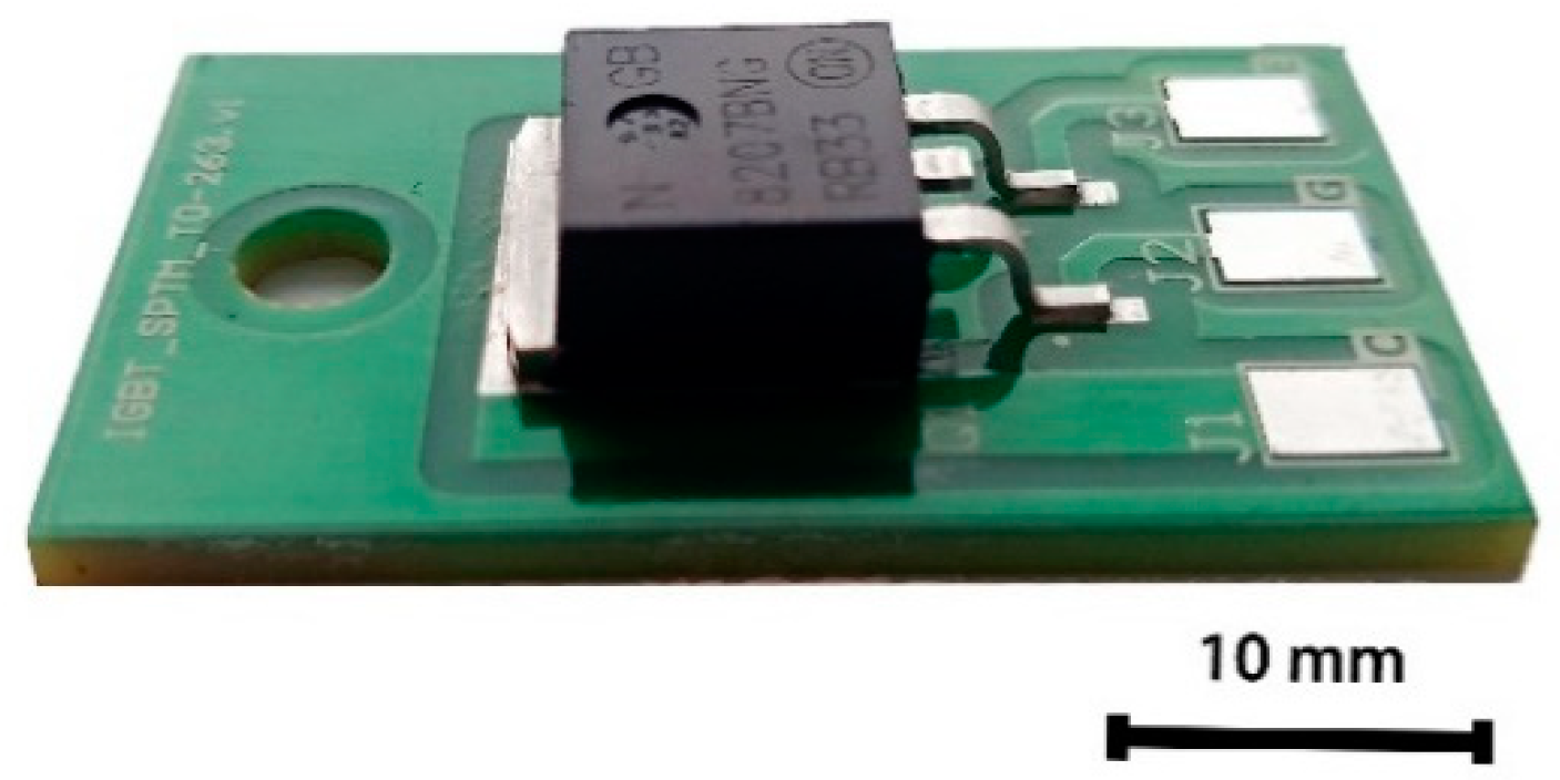
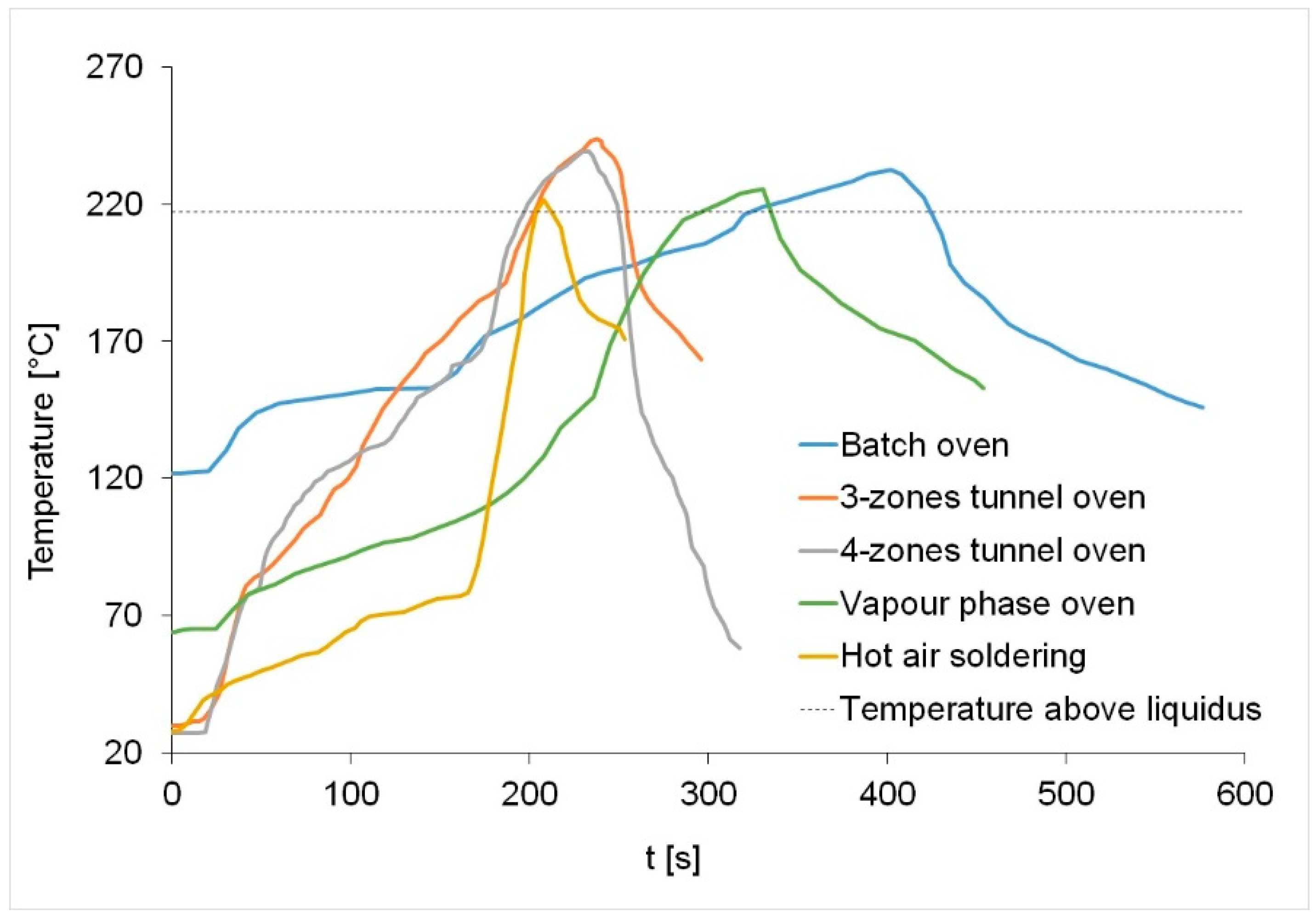
Glass-epoxy laminate (FR4), with a thickness of 1.50 mm (Satland Prototype, Gdańsk, Poland), covered with a 35 μm thick Cu layer, was used as a substrate. The surface finishing was prepared from the hot air leveling (HAL) Sn99Cu0.7Ag0.3 layer with a thickness of 1 ÷ 40 μm. IGBT transistors NGB8207BN (VCES = 365 V, ICmax = 20 A, TL = 275 °C, package TO-263, ON Semiconductor, Phoenix, Arizona, USA) were soldered onto the substrates with SACX0307 (Sn99Ag0.3Cu0.7) paste (LOCTITE HF 212, Henkel Adhesives, Düsseldorf, Germany) (Figure 2).The solder joints were prepared using stencil printing with a stencil thickness of 125 µm. To prevent a short circuit from forming during the soldering, the stencil aperture was narrowed by 10% over the thermal pad. The samples were soldered with different soldering ovens: a batch oven, convection reflow ovens 3-zones SMT 460C (Essemtec AG, Aesch, Switzerland), 4-zones (TWS AUTOMATION, Avenza, Italy), and a vapour phase soldering oven (ASSCON Quicky 450 VPS, Königsbrunn, Germany). The thermal profiles of the soldering processes are shown in Figure 3, and a detailed description of them is given in Table 1. The thermal profiles were measured at a soldering pad of the PCB, typically at the terminals of the IGBT. For the purposes of comparison, the samples were soldered with hot air (Infrared Preheater Quick 854ESD and Lead-Free Rework Station QUICK856AE, Quick Soldering Co. Ltd., Changzhou, China). Five samples were fabricated in each oven. Single-factor variance analysis and Tukey’s test were performed using Statistica software (TIBCO Software Inc, CA, -USA) at a significance level (α) of 0.05.

2.2. Thermal Measurements

The thermal impedance Zth(t) and thermal resistance Rth of the samples were measured. For this purpose, the measuring set-up, shown in Figure 4, was used [16]. An indirect electrical method was used based on gate-emitter voltage VGE as a thermo-sensitive parameter [17]. During the measurements, the FR4 substrate with soldered IGBT was fixed to a liquid-cooled heat exchanger [18] to increase the cooling efficiency of the FR4 substrate [19].
In the measuring set-up, the thermal impedance Zth(t) was determined in three steps.
  • Calibration of the thermometric characteristic. The characteristic describes the dependence of a thermo-sensitive parameter on temperature. The calibration was performed at a closed switch (S1). The measurement current (IM) of 1.3 mA flowed through the transistor. During calibration, the temperature of the transistor was regulated by a thermostat, in which the device being tested was situated. The slope of the thermometric characteristic was calculated on the basis of this characteristic;
  • Heating. In the second step of measurements, the heating power was dissipated in the transistor operating within the active range, and its internal temperature increased as a result of self-heating. In this stage, switch (S1) was opened. The current IH flowed through the self-heating device. This step ended after a thermally steady-state was obtained. At this point, junction temperature of the transistor should be around 100 °C. At the steady-state, the value of the voltage drop (VCE) in the self-heating device was measured. The value of heating power (PH) was equal to the product of the voltage drop of the self-heating device and current IH. In the case of the performed measurements, it was equal to 4.9 W;
  • Cooling. This step began after the change in the state of the switch S1 at time t = 0 and meant the measurement of the waveform of the thermo-sensitive parameter until the steady-state was obtained. Then, the current flowed through the transistor, which was equal to the calibration value. VGE voltage was measured at defined time intervals with an analogue-to-digital (A/D) converter and recorded by a PC. The waveform of junction temperature (Tj) of the IGBT were calculated according to the use of the thermometric characteristic measured during calibrations and the waveform of voltage VGE(t) measured in the third step of measurements. Finally, the transient thermal impedance was calculated using the following equation:
    Z t h ( t ) = T j ( t ) T a P H
    where Tj is junction temperature, Ta is ambient temperature and PH is heating power.
Thermal resistance Rth corresponds to the values of thermal impedance Zth(t) at the steady-state.

2.3. Investigations of the Solder Joints

For void identification, a 2-dimensional (2D) static imaging technique was employed using Micro-CT Imaging. All X-ray measurements were performed using a GE Sensing & Inspection Technologies Phoenix X-ray Gmbh “Nanotom 180 N” (Waygate Technologies, Hürth, Germany). The temperature distribution inside the test samples was measured using a thermo-vision camera FLIR i5 (InfraTec, Dresden, Germany). The microstructure of the solder joints was investigated on metallographic cross-sections using optical microscopy (Olympus BX50, Tokyo, Japan) and Scanning Electron Microscopy (FEI Inspect S50, Thermo Fisher Scientific, Waltham, MA, USA).

3. Results and Discussion

The values of thermal resistance Rth, and the waveforms of transient thermal impedance Zth(t) for different samples are presented in Figure 5 and Figure 6. In Figure 5, the small squares represent the average; the horizontal lines indicate the median; the borders of the boxes indicate the ±σ standard deviation; the crosses mark the min–max values. The differences in thermal resistances were observed.
Single-factor variance analysis of the results proved that there were statistically important differences between the samples at a significance level of 0.05. The letters A, B, and C in Figure 5 mean statistically important differences between the samples. According to Tukey’s test, the samples soldered in a batch oven had the lowest thermal resistance, which was surprising, and they differed significantly from all of the other samples. Thermal resistance in the case of the tunnel ovens was slightly but statistically higher. The highest values were obtained from the samples soldered in the vapour phase (VPS) oven and manually with hot air. As was proven earlier, vapour phase soldering can be a very effective soldering method, especially for large-component soldering, but it has some limitations. First of all, because of the intensive heating, solder joints performed with VPS can exhibit greater voiding and tombstone failures. A vacuum option seems to be necessary for this type of soldering. Without the application of underpressure in the last 5 s of soldering, the quality and the solder joint was much worse [12,20].
The results of the transient thermal impedance (Figure 6) showed differences in the course of the curves after 10s for the different soldering ovens, which reached 15% between the samples. This is due to the fact that solder joints are responsible for the longest thermal time constant of the IGBTs under investigation. Before 10s, the smaller differences in the curves are the only measurement errors.
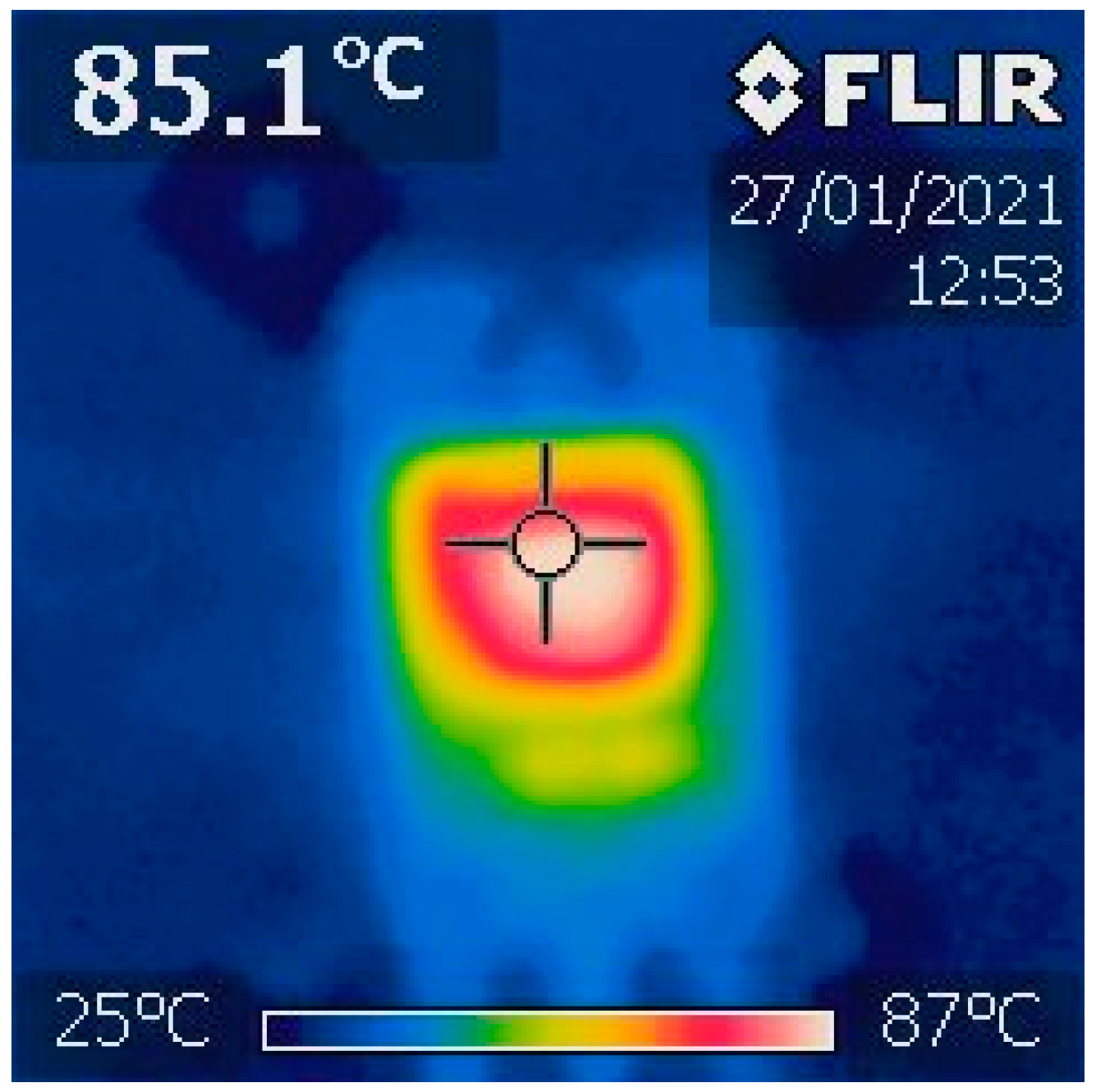
Figure 7 shows a thermal image of a transistor which was soldered in the batch oven. The heat distribution was similar for all the samples. Heat was effectively removed from the transistor by the liquid flowing through the heat exchanger. A large temperature gradient was observed between the edges of the sample and the middle. The temperature of the FR4 substrate started to decrease considerably from 4 mm from the IGBT component and did not exceed 30 °C. The temperatures of the exchanger and the liquid flowing through it were close to the ambient temperature. The detected temperature maximum was 15 °C higher than the measured junction temperature. This was due to the difference between junction and case temperatures of the IGBT, which was particularly visible in the conditions where the device being tested was effectively cooled [21]. Moreover, such a high value of discrepancy may also be affected by averaging the temperature over an area larger than the structure of the transistor, which is the heat source used by the infrared camera [22]. This suggests that our measurement method (Figure 4) is more accurate and suitable for microelectronics applications than the frequently used thermo-vision camera.
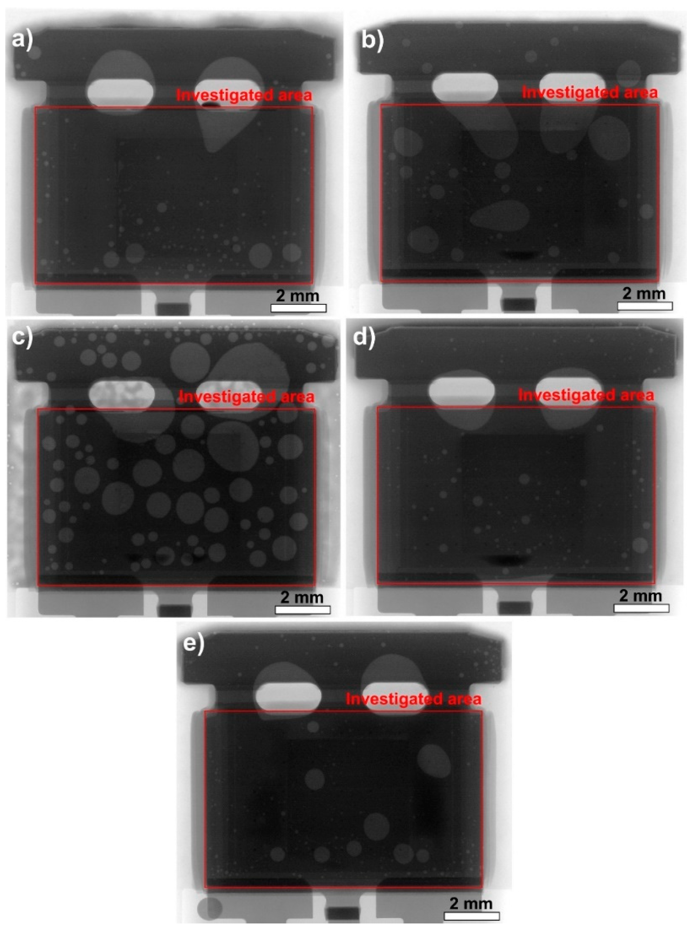
The voids ratio for the samples is presented in Figure 8 and Table 2. While the voids were being calculated, only the area of the thermal pad was taken into account; since most of the heat was dissipated here, it is marked by a rectangle in Figure 8. The voids percentage differed significantly. The highest voids percentage area was observed for the samples soldered in a 4-zones tunnel oven, reaching 30%. For the rest of the samples, this parameter did not exceed 12%. However, the standard deviation was relatively high.
As was assumed, the reason for the increase in Rth could be the increase in voids in the solder joints. Empty spaces in a metal structure could act like insulation. However, interestingly, the voids ratio did not correspond to the results of Rth measurements. The highest Rth values were observed for the samples soldered in a VPS oven and manually with hot air. It suggested that the voids ratio in the solder joint, up to a threshold of 30%, was not a crucial parameter affecting the thermal management of the IGBTs. The worst VPS results were not caused by the limiting effect of the vapour on the possibility of effective flux outgassing during the soldering process, as was suspected.
The increase in Rth values was probably caused by the microstructure changes in the solder joint. Typically, the SAC solder joints are composed of the β–Sn matrix and intermetallic compounds (IMCs), such as Cu6Sn5, Cu3Sn, and Ag3Sn [23]. IMCs presented both in the solder bulk as isolated dissolved islands and as an IMC layer (typically Cu6Sn5) between Cu pad and solder alloy. The microstructure, especially IMC presence, changed the thermal and electrical parameters of solder joints.
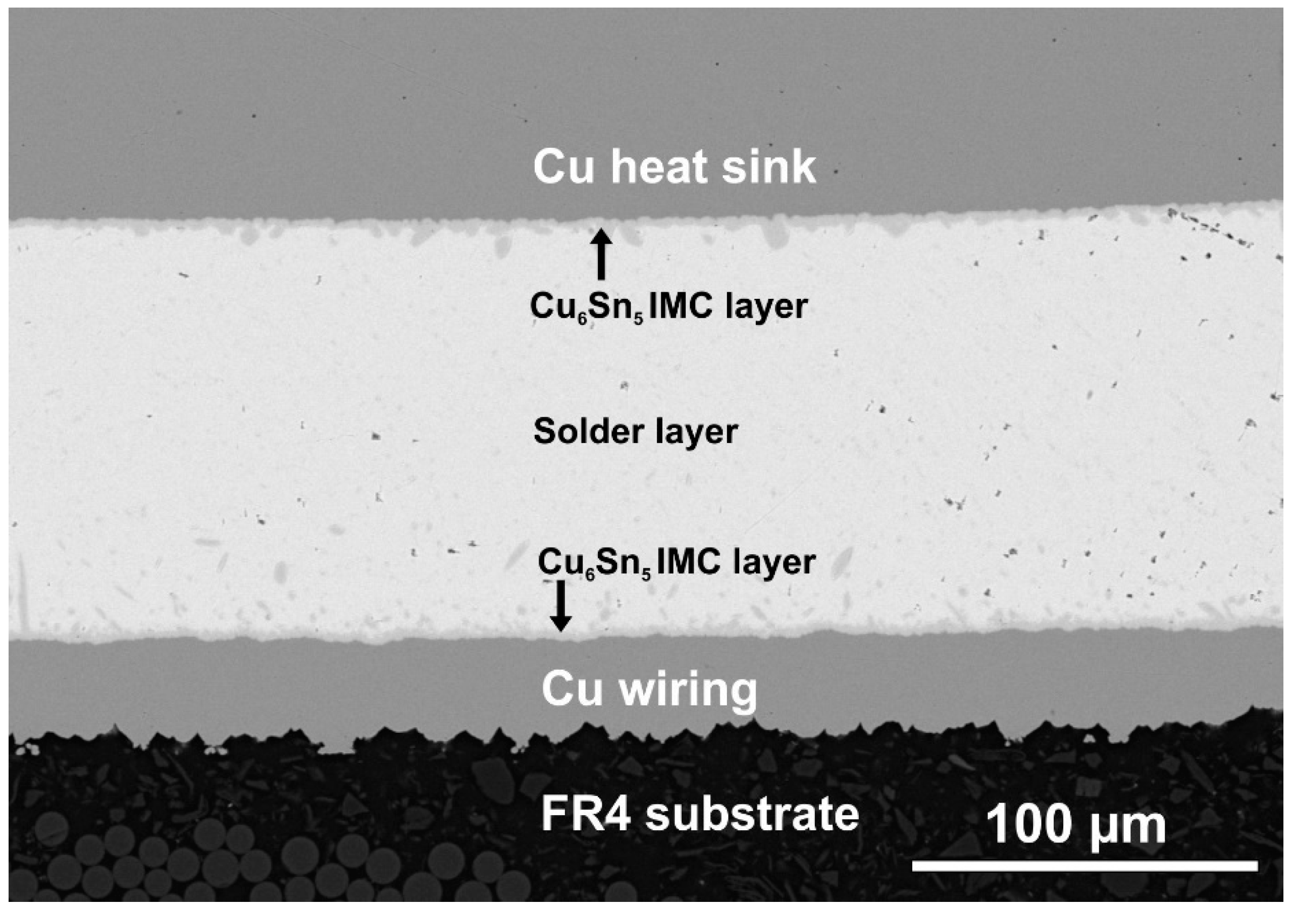
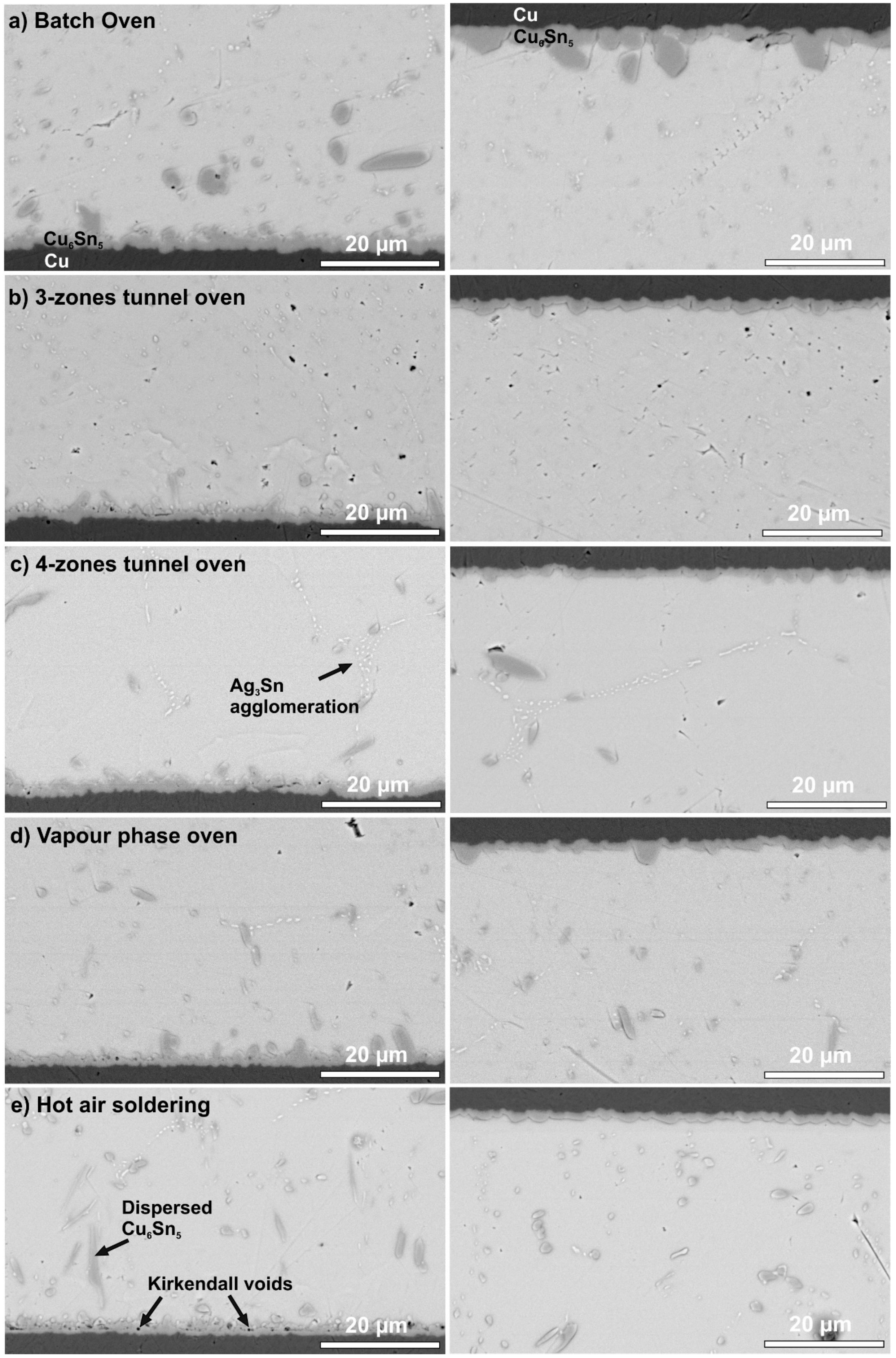
The structure of the solder joints can be seen in Figure 9. It can be described “a sandwich” structure, with upper and bottom parts. The upper part meant the interface between the component (transistor) and the solder joint, the bottom part corresponded to the interface between the solder joint and the FR4 substrate. According to the statistical evaluation, the thickness of the solder joints was 122.1 ± 12.6 µm. Both interfaces contained a Cu layer, which takes part in the formation of IMC layers. The microstructural analysis of the solder joints can be seen in Figure 10. Generally, the microstructure of the solder joints was similar, but some differences also occurred. The IMC layer was the thickest in the case of the batch oven (Figure 10a). It reached 3 µm at the upper side of the solder joints; in the other cases, the typical thickness was under 2 µm on both sides of the solder joint. A high amount of agglomerated Ag3Sn was found at β-Sn grain boundaries in the case of the 4-zones tunnel oven (Figure 10c). This is unusual in the case of a low-Ag content solder alloy. In the other cases, only evenly distributed Ag3Sn dots are visible at the Sn grain boundaries. According to the distribution of the Ag3Sn IMCs, the size of the β-Sn grains can be approximated (since the Ag3Sn IMCs are located at the grain boundaries [14]). The β-Sn matrix was the finest (<20 µm) in the case of the 3-zones tunnel oven. Soldering in the batch oven and the hot air soldering resulted in an average grain size of around ~20 µm. The largest grains (>40 µm) were observed for the samples soldered in a 4-zones tunnel oven and with vapour phase soldering. The number of dispersed Cu6Sn5 islands was the highest in the case of the batch oven and the hot air soldering. In the case of the hot air soldering, Kirkendall voids were found in the lower interface of the Cu base and the IMC layer, which could have formed due to the rapid heat flow into solder joints (Figure 3).
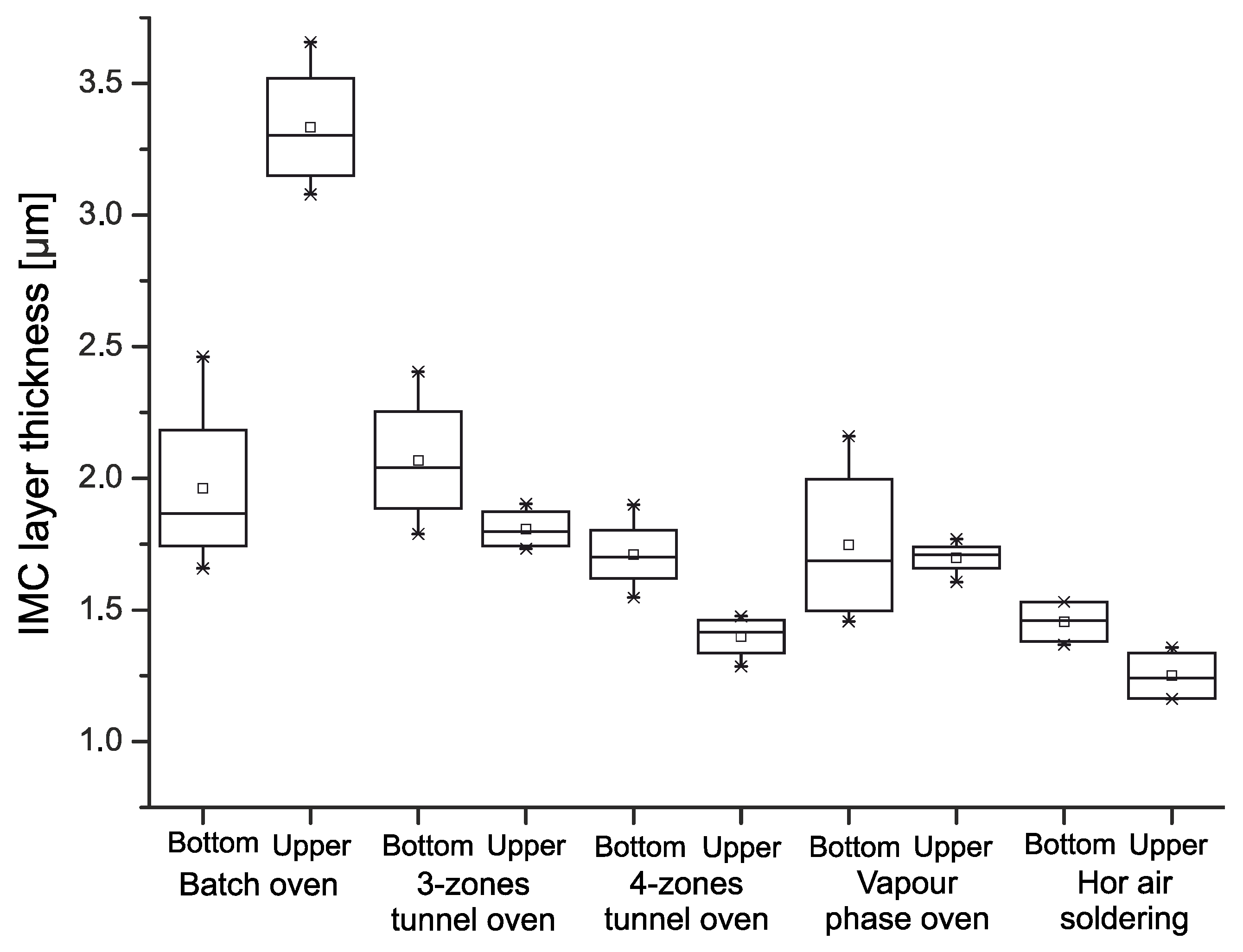
A deeper analysis of the IMC layer thicknesses can be seen in Figure 11. Considerable IMC thickness differences have been found between the soldering technologies, which correlate well with the “time above liquidus” during the soldering process. Time above liquidus means the time that the solder joint spends in the liquid state during the reflow process, practically the time above the liquidus point of the applied solder alloy. In our case, it was the time above 217 °C (SACX0307 solder alloy). The time above liquidus values can be calculated from the thermal profiles (Figure 3) for all samples. The longer liquid state of the solder results in a thicker IMC layer [15]. If we compare the thermal profiles (Figure 3) with the average IMC thicknesses (Figure 11), it can be concluded that they correlate well. Usually, the IMC layer was a little thicker at the bottom side of the solder joint than at the upper side. The only exception was the batch oven. Interestingly, the Rth values (Figure 5) are inversely proportional to the IMC layer thicknesses (Figure 11). The lowest Rth values were measured in the case of the batch oven (~15 K/W) with the thickest IMC layers (bottom and upper together over 5 µm). The highest Rth values were measured in the case of the vapour phase and hot air soldering (~18K/W) with the thinnest IMC layers (lower and upper together around ~3 µm). The specific thermal properties of the bulk SnAgCu solders and the Cu6Sn5 IMC are around 55–60 W/mK [24] and 34 W/mK [25]. However, recent studies have proved that bonded Cu-Sn IMC joints made by solid–liquid interphase diffusion could reach specific thermal conductivity of between 120 and 140 W/mK [26,27]. Therefore, the role of the IMC layer in the heat transfer of solder joints needs further and deeper investigation, since it is surely not negative, as our results also showed.

4. Conclusions

The effect of solder joint preparation on the thermal properties of the IGBT soldered on FR4 substrate was investigated. It was found that both the soldering technology used and the thermal profile could change the thermal impedance Zth(t) and thermal resistance Rth. The differences were between 15% and 20% for Zth(t) and Rth, respectively. The best results were observed in the case of a batch oven with infrared heating. Although the ratio of the gas void in the solder joints varied between 3% and 30%, no correlation between the void ratios and Rth value increase was found. This means that, in the case of the power package TO263, the void ratio of the solder joint is not as important from the perspective of the proper working of the component, as was supposed by the microelectronics industry. The microstructure of the solder joint showed significant differences in IMC layer thicknesses in the case of the different soldering technologies, which correlated well with the time above liquidus during the soldering process. The thermal parameters of the IGBT soldered onto the FR4 substrate could be changed due to the increased thermal conductivity of the IMC layer as compared to that of the bulk solder joint. Our research highlighted the importance of the soldering technology used and the thermal profile in the case of IGBT components.

Author Contributions

Conceptualization (A.S. and P.G.); methodology (A.S. and P.G.); validation (P.G., A.P., S.W. and B.I.), investigation, (A.S., P.G., A.P., S.W. and B.I.); resources, (A.S., P.G. and A.P.); writing—original draft preparation, (A.S., P.G. and A.P.); writing—review and editing, (A.S. and P.G.); visualization, (A.S., P.G., A.P. and B.I.).; supervision, (A.S.); funding acquisition, (A.S., P.G.) All authors have read and agreed to the published version of the manuscript.

Funding

The work of Agata Skwarek and Paweł Górecki was financed within the program of the Ministry of Science and Higher Education called “Regionalna Inicjatywa Doskonałości” in the years 2019–2022, the project number 006/RID/2018/19, the sum of financing 11 870 000 PLN”. The work of Balázs Illés was partially supported by the National Research Development and Innovation Office—Hungary (NKFIH) as part of project no FK 127970.

Institutional Review Board Statement

Not applicable.

Informed Consent Statement

Not applicable.

Data Availability Statement

For detailed data presented in this study please contact the corresponding author.

Conflicts of Interest

The authors declare no conflict of interest.

References

  1. Illés, B.; Horváth, B. Tin Whisker Growth from Micro-alloyed SAC Solders in Corrosive Climate. J. Alloys Comp. 2014, 616, 116–121. [Google Scholar] [CrossRef]
  2. Diehm, R.; Nowottnick, M.; Pape, U. Reduction of voids in solder joints an alternative to vaccum soldering. In Proceedings of the IPC APEX EXPO, San Diego, CA, USA, 28 February–1 March 2012. [Google Scholar]
  3. Iwamuro, N.; Laska, T. IGBT history, state-of-art and future prospects. IEEE Trans. Electron Devices 2017, 64, 741–752. [Google Scholar] [CrossRef]
  4. Baliga, B.J. Fundamentals of Power Semiconductor Devices, 2nd ed.; Springer: Raleigh, NC, USA, 2019; pp. 755–756, 759–760. [Google Scholar]
  5. Du, M.; Guo, Q.; Ouyang, Z.; Wei, K.; Hurley, W.G. Effect of solder layer crack on the thermal reliability of Insulated Gate Bipolar Transistors. Case Stud. Therm. Eng. 2019, 14, 100492. [Google Scholar] [CrossRef]
  6. Zhu, Y.; Xiao, M.K.; Su, X.Z.; Yang, G.; Lu, K.; Wu, Z.H. Modeling of Conduction and Switching Losses for IGBT and FWD Based on SVPWM in Automobile Electric Drives. Appl. Sci. 2020, 10, 4539. [Google Scholar] [CrossRef]
  7. Choi, U.M.; Blaabjerg, F.; Jørgensen, S.; Iannuzzo, F.; Wang, H.; Uhrenfeldt, C.; Munk-Nielsen, S. Power cycling test and failure analysis of molded Intelligent Power IGBT Module under different temperature swing durations. Microelectron. Reliab. 2016, 64, 403–408. [Google Scholar] [CrossRef]
  8. Górecki, K.; Ptak, P. Influence of the area of a thermal pad on optical and thermal parameters of LED modules. Circuit World 2020, 46, 65–70. [Google Scholar] [CrossRef]
  9. Catalano, A.P.; Scognamillo, C.; d’Alessandro, V.; Castellazzi, A. Numerical Simulation and Analytical Modeling of the Thermal Behavior of single- and Double Sided Cooled Power Modules. IEEE Trans. Comp. Packag. Manuf. Technol. 2020, 10, 1446–1453. [Google Scholar] [CrossRef]
  10. Coombs, C.F., Jr. Printed Circuits Handbook, 6th ed.; McGRAW-HILL: New York, NY, USA, 2008. [Google Scholar]
  11. Jiang, M.; Fu, G.; Wan, B.; Xue, P.; Qiu, Y.; Li, Y. Failure analysis of solder layer in power transistor. Solder. Surf. Mount Technol. 2018. [Google Scholar] [CrossRef]
  12. Skwarek, A.; Illés, B.; Synkiewicz, B.; Wroński, S.; Tarasiuk, J.; Witek, K. Characterization of solder joints made with VPS on DBC substrate. J. Mater. Sci. Mater. Electron. 2017, 28, 1769–1776. [Google Scholar] [CrossRef]
  13. Nowottnick, M.; Novikov, A.; Pape, U. Material-und prozesseinfluesse auf die herstellung porenarmer loetverbindungen. SMT Hybrid Packag. Tutor. 2007, 11. [Google Scholar]
  14. Skwarek, A.; Ptak, P.; Górecki, K.; Hurtony, T.; Illés, B. Microstructure Influence of SACX0307-TiO2 Composite Solder Joints on Thermal Properties of Power LED Assemblies. Materials 2020, 13, 1563. [Google Scholar] [CrossRef] [PubMed]
  15. Busek, D.; Dusek, D.; Beran, T.; Vesely, P. Thermo-mechanical test of SnBi and SnCu solder joints on different surface finishes. In Proceedings of the 42nd IEEE-ISSE conference, Wroclaw, Poland, 15–19 May 2019. [Google Scholar] [CrossRef]
  16. Górecki, P.; Górecki, K. Measurements and Computations of Internal Temperatures of the IGBT and the Diode Situated in the Common Case. Electronics 2021, 10, 210. [Google Scholar] [CrossRef]
  17. Avenas, Y.; Dupont, L.; Khatir, Z. Temperature Measurement of Power Semiconductor Devices by Thermo-Sensitive Electrical Parameters—A Review. IEEE Trans. Power Eelctronics 2012, 27, 3081–3092. [Google Scholar] [CrossRef] [Green Version]
  18. Ptak, P.; Gorecki, K.; Skwarek, A.; Witek, K.; Tarasiuk, J. The influence of soldering process parameters on the optical and thermal properties of power LEDs. Solder. Surf. Mount Technol. 2020, 32, 191–199. [Google Scholar] [CrossRef]
  19. Catalano, A.P.; Trani, R.; Scognamillo, C.; d’Alessandro, V.; Castellazzi, A. Optimization of thermal vias design in PCB-based power circuits. In Proceedings of the 21st International Conference on Thermal, Mechanical and Multi-Physics Simulation and Experiments in Microelectronics and Microsystems EuroSimE, Cracow, Poland, 5–8 July 2020. [Google Scholar]
  20. Illés, B.; Géczy, A.; Skwarek, A.; Bušek, D. Effects of substrate thermal properties on the heat transfer coefficient of vapour phase soldering. Int. J. Heat Mass Trans. 2016, 101, 69–75. [Google Scholar] [CrossRef]
  21. Górecki, K.; Górecki, P. The Analysis of Accuracy of the Selected Methods of Measuring Thermal Resistance of IGBTs. Metrol. Meas. Syst. 2015, 22, 455–464. [Google Scholar] [CrossRef] [Green Version]
  22. Susinni, G.; Rizzo, S.A.; Iannuzzo, F. Two Decades of Condition Monitoring Methods for Power Devices. Electronics 2021, 10, 683. [Google Scholar] [CrossRef]
  23. Yahaya, M.Z.; Nazeri, M.F.M.; Kheawhom, S.; Illés, B.; Skwarek, A.; Mohamad, A.A. Microstructural analysis of Sn-3.0Ag-0.5Cu-TiO2 composite solder alloy after selective electrochemical etching. Mater. Res. Express 2020, 7, 016583. [Google Scholar] [CrossRef]
  24. Zhang, Z.; Cao, H.; Xiao, Y.; Cao, Y.; Li, M.; Yu, Y. Electromigration-induced growth mode transition of anodic Cu6Sn5grains in CujSnAg3.0Cu0.5jCu lap-type interconnects. J. Alloys Compd. 2017, 703, 1–9. [Google Scholar] [CrossRef]
  25. Frederikse, H.P.R.; Fields, R.J.; Feldman, A. Thermal and electrical properties of coppertin and nickeltin intermetallics. J. Appl. Phys. 1992, 72, 2879–2882. [Google Scholar] [CrossRef]
  26. Greve, H.; McCluskey, F.P. Thermal conductivity of Cu-Sn transient liquid phase sintered interconnects for high power density modules. In Proceedings of the 2017 International Workshop on Integrated Power Packaging (IWIPP), Delft, The Netherlands, 5–7 April 2017; pp. 1–7. [Google Scholar]
  27. Lee, B.-S.; Yoon, J.-W. Cu-Sn Intermetallic Compound Joints for High-Temperature Power Electronics Applications. J. Electron. Mater. 2018, 47, 430–435. [Google Scholar] [CrossRef]
Figure 1. A simplified diagram of the heat flow through the component to the FR4 substrate. The arrows show an example of the direction of heat dissipation.
Applsci 11 05583 g001
Figure 2. Test sample of NGB8207BN transistors soldered onto FR4 substrate.
Applsci 11 05583 g002
Figure 3. Soldering thermal profiles.
Applsci 11 05583 g003
Figure 4. Transient thermal impedance Zth(t) measurement set-up scheme.
Applsci 11 05583 g004
Figure 5. Thermal resistance (Rth) of NGB8207BN transistors soldered onto FR4 substrate in different soldering ovens.
Applsci 11 05583 g005
Figure 6. Transient thermal impedance waveforms of NGB8207BN transistors soldered onto FR4 substrate in different soldering ovens.
Applsci 11 05583 g006
Figure 7. An exemplary thermal image of NGB8207BN transistors soldered in a batch oven.
Applsci 11 05583 g007
Figure 8. X-ray images of the solder joints under the IGBT: (a) batch oven, (b) 3-zones tunnel oven, (c) 4 zones tunnel oven, (d) vapour phase oven, (e) hot air soldering.
Applsci 11 05583 g008
Figure 9. An exemplary “sandwich structure” of the solder joints under IGBT soldered in batch oven (SEM micrograph).
Applsci 11 05583 g009
Figure 10. SEM micrographs of the solder joints under the IGBT: (right bottom side of the solder joint, left upper side of the solder joint): (a) batch oven, (b) 3-zones tunnel oven, (c) 4-zones tunnel oven, (d) vapour phase oven, (e) hot air soldering.
Applsci 11 05583 g010
Figure 11. The IMC layer thicknesses of the solder joints soldered in different soldering ovens.
Applsci 11 05583 g011
Table 1. Soldering ovens.
SolderingType of HeatingTemperature (°C)Time (s)Atmosphere
Batch ovenInfrared radiationpre-heating 150–180 140 Air
reflowing 210–254 200
cooling 254–170180
3-zones tunnel ovenConvectionpre-heating 160–180 60 Air
reflowing 213–247 40
cooling 247–15070
4-zones tunnel ovenConvectionpre-heating 140–175 50 Air
reflowing 210–240 50
cooling 240–14030
Vapour phase ovenHeat conductionpre-heating 125–187 50 Inert
reflowing 206–227 60
cooling 227–150130
Hot air solderingConvectionpre-heating 120–195 15 Air
reflowing 195–221 10
cooling 221–17550
Table 2. Voids percentage area.
SolderingAverage Void Ratio (%)
Batch oven6.9 ± 1.5
3-zones tunnel oven12.8 ± 6.7
4-zones tunnel oven30.9 ± 4.9
Vapour phase oven11.2 ± 4.6
Hot air soldering3.6 ± 2.2
Publisher’s Note: MDPI stays neutral with regard to jurisdictional claims in published maps and institutional affiliations.