Article

Experimental Validation of Formula for Calculation Thermal Diffusivity in Superlattices Performed Using a Combination of Two Frequency-Domain Methods: Photothermal Infrared Radiometry and Thermoreflectance

1
Institute of Physics, Faculty of Physics, Astronomy and Informatics, Nicolaus Copernicus University, Grudziadzka 5, 87-100 Torun, Poland
2
Chair of Applied Solid-State Physics, Experimental Physics VI, Ruhr-University Bochum, Universitaetsstrasse 150, D-44780 Bochum, Germany
*
Author to whom correspondence should be addressed.
Appl. Sci. 2021, 11(13), 6125; https://doi.org/10.3390/app11136125
Submission received: 21 May 2021 / Revised: 25 June 2021 / Accepted: 26 June 2021 / Published: 30 June 2021
(This article belongs to the Special Issue Recent Advances in Application of Coatings and Films)

Abstract

:
In this paper, we validate two theoretical formula used to characterize thermal transport of superlattices at different temperatures. These formulas are used to measure cross-plane thermal conductivity and thermal boundary resistance, when it is not possible to obtain heat capacity or thermal diffusivity and in-plane thermal conductivity. We find that the most common formula for calculating thermal diffusivity and heat capacity (and density) can be used in a temperature range of −50 °C to 50 °C. This confirms that the heat capacity in the very thin silicon membranes is the same as in bulk silicon, as was preliminary investigated using an elastic continuum model. Based on the obtained thermal parameters, we can fully characterize the sample using a new procedure for characterization of the in-plane and cross-plane thermal transport properties of thin-layer and superlattice semiconductor samples.

1. Introduction

Quantitative description of heat dissipation in multi-layered nanostructures and thin layers is a challenging task. One of the most popular methods is time-domain thermo-reflectance (TDTR) [1,2,3,4,5,6,7,8,9,10,11,12,13,14]. For superlattices, the strategy for investigating their thermal properties using the TDTR method relies on measuring thermal conductivity. The other cross-plane and in-plane thermal parameters (thermal diffusivity and thermal boundary resistance) are calculated based on this parameter. However, in order to measure the thermal conductivity in the TDTR, method, researchers need to use the heat capacity of the bulk material. A preliminary theoretical investigation, used an elastic continuum model, suggested that the heat capacity in the very thin silicon membranes is the same as in bulk silicon [15]. For superlattices, this relation is more complex. However, frequency-domain measurements are simple and less expensive and can measure all thermal transport properties. The benefit of using frequency domain methods over time-resolved methods is their unique profilometry capability. This relies on the observation that one can relate the origin of a signal at a given frequency to the depth or penetration length of the thermal wave (i.e., thermal diffusion length). This allows the thermal conductivity as a function of depth to be probed by varying the frequency. Another major advantage of frequency domain methods is that they are simpler to implement experimentally and do not require the use of expensive femtosecond lasers. There are many frequency-domain methods, such as photoacoustic [16,17], photothermal beam reflection [18,19], thermoreflectance [20,21] photothermal infrared radiometry [22,23,24,25,26,27,28,29,30], and modulated free carrier absorption [31,32]. Recently, we reported on cross-plane thermal transport properties of superlattices and thin films by using a frequency-domain PTR (photothermal infrared radiometry) method [24]. We demonstrated that it is possible to estimate values of the cross-plane thermal parameters for one-dimensional heat flow. In this paper, we study thin-layer and superlattice samples using both frequency domain methods, PTR and thermoreflectance (FDTR), at different temperatures. The purpose of this study is to demonstrate that both methods are complementary and that all in-plane and cross-plane heat transport properties can be fully measured using both methods. All parameters are then used for the experimental validation of formulas calculating thermal transport properties in superlattice in different temperature.

2. Materials and Methods

2.1. Frequency Domain Photothermal Infrared Radiometry Set Up

The PTR experimental set-up is presented in Figure 1 [24]. The DPSS laser (λ = 532 nm, 800 mW CW power, model CNI laser MGL-FN-532–1W) is intensity-modulated by an acoustic-optical modulator (model Crystal Technology, Inc. AOM 3080-120) in the frequency range between 100 Hz and 10 MHz using a 30 MHz waveform generator (Agilent 33522A). The beam spot (1/e2) has a diameter of 1.8 mm. Two Au-coated off-axial parabolic mirrors are used to collect and collimate the emitted IR radiation from the sample, focusing it on a photoconductive mercury cadmium telluride (MCT) detector (Kolmartech KMPV 11-1-J1/DC/Ge). The detector has peak sensitivity at a wavelength of 9.6 µm and an active area of 1 mm2 (with sensitivity between 2 µm and 12 µm). It is cooled with liquid nitrogen and has an antireflection-coated Ge window. Finally, the signal from the detector is processed by a lock-in amplifier (LIA, SR865 from Stanford Research, able to work in the frequency range between DC and 2 MHz and SR844 in the frequency range of 2 MHz and 10 MHz). Additionally, the system is prepared for temperature-dependent measurements using a Linkam System (LTS420) able to work between −200 °C and 420 °C.
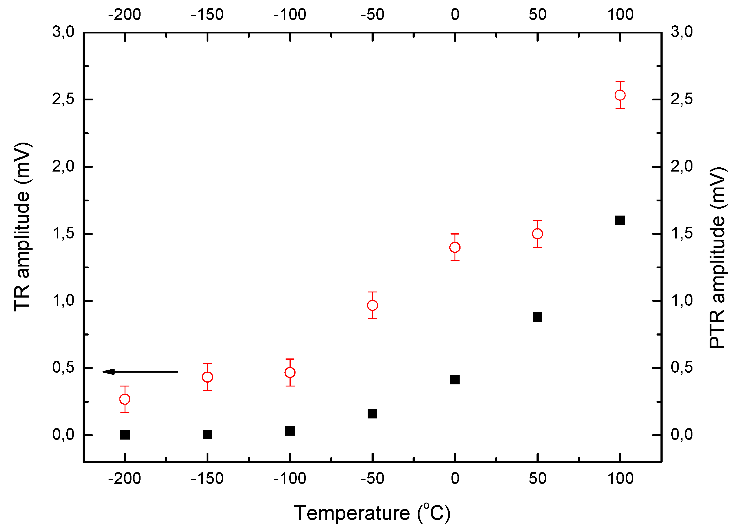
The disadvantage of the PTR method is that the signal strongly decreases with the temperature with law E ~ σ T 3 T (where σ is Stefan-Boltzmann constant) as shown in Figure 2. For comparison, the results from frequency-domain thermoreflectance (FD-TR) measurements are also presented.
Although the PTR signal can be increased by decreasing the beam size, we should bear in mind that there is a trade-off between one-dimensional heat propagation in the sample and the beam spot size. Thus, there is an optimum spot-size that maximizes the PTR signal while keeping the heat-transport one-dimensional. From Figure 2 one can see that at low temperature (below −100° C/173 K), the PTR signal is very small and measurements cannot be taken in frequency-scans up to MHz. On the other hand, thermoreflectance can be measured down to 50 K [33]. The thermoreflectance signal can be described by the formula [33]:
S TR = R R = ( 1 R R T ) T = C TR T
where ΔT is the thermal wave oscillations (which depends on the temperature via thermal transport parameters) and CTR is the thermoreflectance coefficient. In paper [16], authors show that signals above room temperature increase linearly with temperature. In our paper we show that this trend is also observed for lower temperatures for a layered sample. The deviation from linear behavior was already observed by other authors [34].

2.2. Frequency Domain Thermoreflectance Set Up

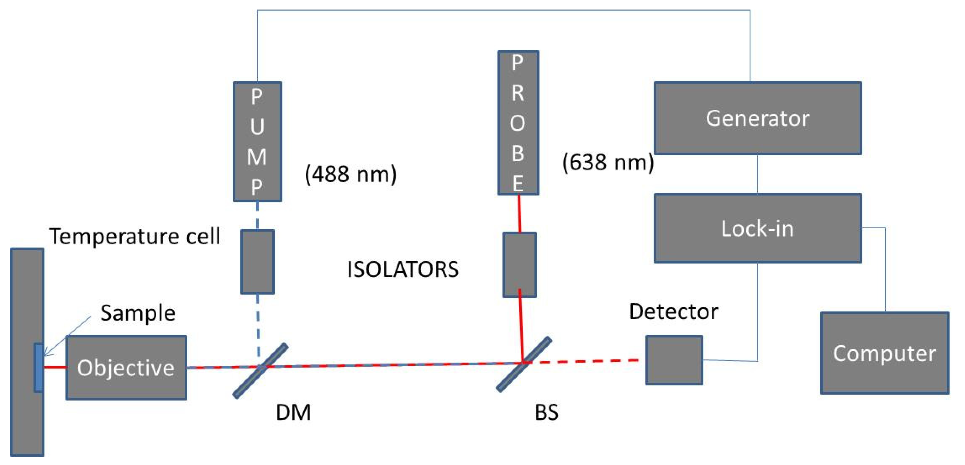
The FD-TR setup is presented in Figure 3.
The 100 mW modulated pump laser (488 nm Cobolt model 06-MLD) was intensity modulated using the sinusoidal signal from the 30 MHz waveform generator (Agilent 33522A). While the 2 mW probe beam (638 nm Cobolt model 06-MLD) was used to monitor the changes of the sample reflectivity due to changes of the temperature induced by the pump beam. The beam spots (1/e2) have been measured (Beam Profiler Slit 2 um S-BR2-Si) to be 3 µm in diameter. Laser beams were focused on the sample by an objective Edmund Optics, 100X model 46-401. The signal was processed by a lock-in amplifier (LIA, SR865 from Stanford Research able to work in the frequency range between DC and 2 MHz). The amplitude A and phase (φ) were acquired, but only the phase was analyzed by a computer for each modulation frequency. The temperature-dependent measurements were performed using a Linkam System able to work between −200 °C and 420 °C. The reference phase was measured by placing the detector instead of the sample. The reference phase was then extracted from the measured phase of the thermoreflectance signal.

2.3. Materials

Sample #1 consisted of a GaAs substrate wafer that was used as a reference. Samples #2 consisted of Al0.33Ga0.67As thin film alloys grown on GaAs substrate wafers while samples #3 and #4 consisted of AlAs/GaAs superlattices grown on GaAs substrate wafers. The GaAs substrate wafers had a 3” (76 mm) diameter with a (001)-orientation and were nominally undoped. The AlxGa(1 − x)As semiconductor alloys and superlattice samples were grown via molecular beam epitaxy (MBE). The GaAs substrate temperature in the MBE chamber during growth was 600 °C (measured by a pyrometer) and the As-flux (beam equivalent pressure BEP) was 9.6 × 10⁻⁶ Torr in the MBE machine. The growth of all wafers was proceeded by careful oxide desorption at 600 °C and the growth of a GaAs buffer layer. The metal layers were deposited by thermal evaporation in a separate deposition chamber with current-heated evaporation boats. Sample #2 had a 200 nm GaAs buffer layer with a nominally 2000 nm thick Al0.33Ga0.67As layer. Sample #3 and #4 and D had a 150 nm GaAs buffer layer and a superlattice consisting of 10 repetitions of nominally 26 nm AlAs and 26 nm GaAs (with the superlattice ending with a GaAs layer). Samples #2 and #4 were covered by a 100 nm thin Au-layer, while sample #1 and #3 are covered by a Ti layer with a thickness of 50 nm. The deposition processes on all samples were done in a vacuum with pressure less than 10−6 mbar.
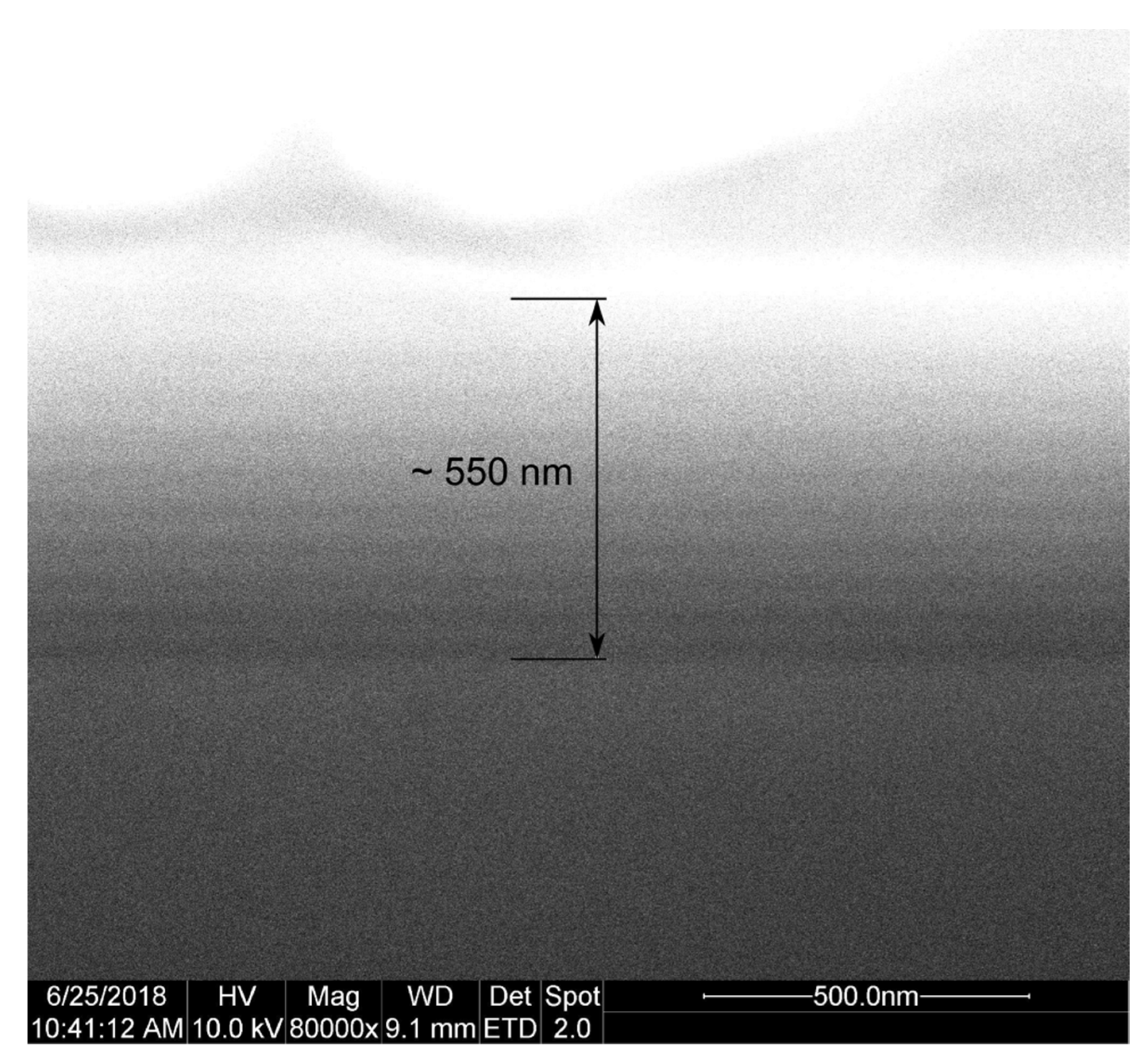
Figure 4 presents Scanning Electron Microscope image (SEM) of superlattice sample.
The difference in film thickness measurements using SEM and reflectometry is due to slight differences in film thickness across the sample surface. The samples measured using reflectometry were used for the measurements. The samples properties are presented in Table 1.

3. Theoretical Models

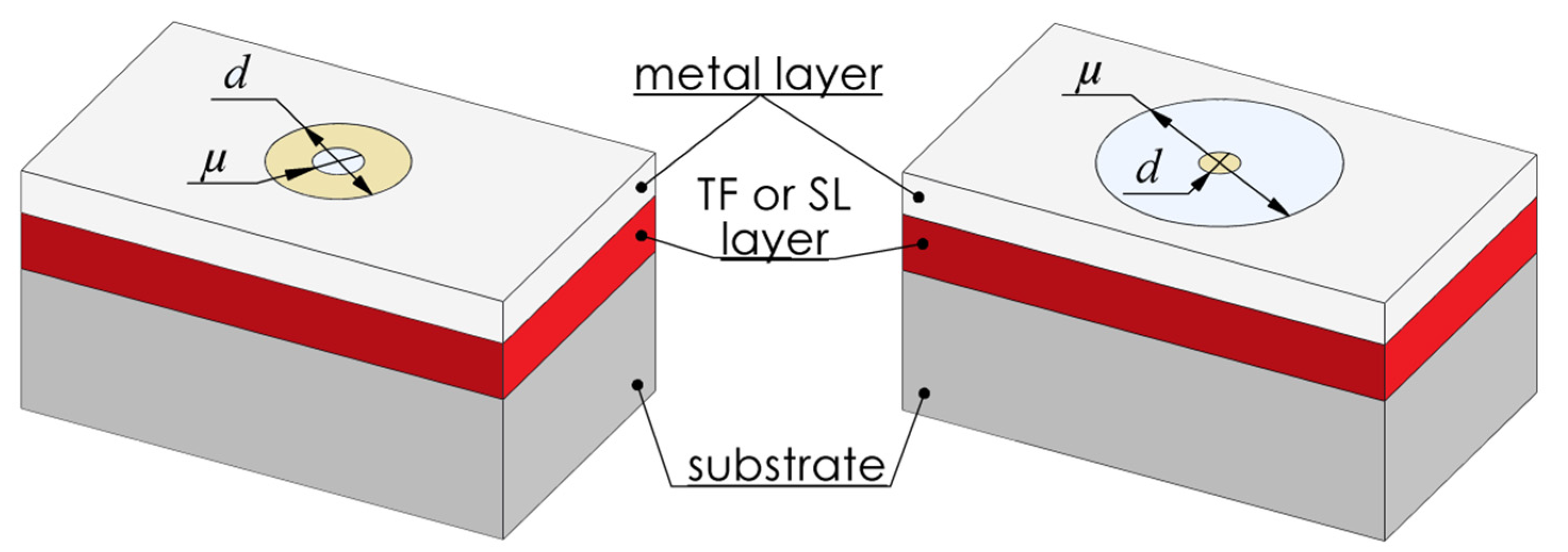
As shown in Figure 5 we used two geometries: cross and in-plane. In-plane geometry is achieved by significantly reducing the width of the excitation beam.
Although Figure 5 suggests that the lower the frequency the better the measurement of in-plane thermal conductivity, it still depends on the thermal parameters (the better the parameter determination sensitivity, range shifts toward higher frequencies, see Figure 6). The three–dimensional signal can be written based on the models already developed and published literature in [23]:
Θ ( ω , 0 ) = Q 2 π 0 D ( λ ) C ( λ ) e ( λ w 0 ) 2 8 λ d λ
where Q is the laser power and w0 is the laser spot 1/e2. The coefficient C and D can be calculated using:
[ A ( λ ) B ( λ ) C ( λ ) D ( λ ) ] = A 3   M 32 A 2 M 21 A 1
Each layer in the model is described by matrices A3, A2, A1 specified by:
A n = [ cos h ( q n d n ) 1 k zn sin h ( q n d n ) k zn q n sin h ( q n d n ) cos h ( q n d n ) ]
Here dn is the layer thickness and kzn the cross-plane thermal conductivity of the nth layer, and:
q 2 = k rn λ 2 + ρ n c n i ω k zn
where ρn is the density of the nth layer, cn is the specific heat capacity of the nth, and krn and kzn are the in-plane and cross-plane thermal conductivities of the nth layer, respectively. For calculations, we used the thermal diffusivity, defined as:
  α zn = k zn ρ n c n
The resistances of the thermal interfaces are described by matrices:
M n , n 1 = [ 1 R n , n 1 0 1 ]
where Rn,n−1 is the thermal interface resistance between the nth and the (n − 1)th layer.
In turns, one-dimensional PTR signal can be written as [24]:
θ ( ω , 0 ) = ( ( 1 R ) I o 2 k 1 σ 1 ) ( 1 + y 1 1 y 1 )
Here, y 1 is a dimensionless quantity defined and σ i = i ω / α i as:
y 1 =   e 2 L 1 σ 1 ( U 1 + U 1 )
where L 1 =   x 1 is the length of first layer and U 1 ± is another dimensionless quantity defined as:
U 1 ± = ( 1 + y 2 )   R 12 k 2 σ 2 ( y 2 1 ) ± ( k 2 σ 2 k 1 σ 1 ) ( y 2 1 )
The multi-layer solution takes the form of a recursive sequence. For the nth layer, the dimensionless quantity y n is defined as:
y n =   e 2 L n σ n ( U n + U n )
where L n = x n   x n 1 and U n ±   is a dimensionless quantity defined as:
U n ± = ( 1 + y n + 1 )   R n , n + 1 k n + 1 σ n + 1 ( y n + 1 1 ) ± ( k n + 1 σ n + 1 k n σ n ) ( y n + 1 1 )

4. Results

It is worth emphasizing that the in-plane thermal conductivity can be measured by either changing the spot-size of the laser on the sample or spatially separating the position of the pump and probe spots [21,35]. Moreover, using the TD-TR method it is not possible to measure the in-plane thermal conductivity by changing its spot size, but one can perform measurements using separation of beams or by the elliptical-beam method [36]. It was found that for time-domain methods the recommended method is to spatially separate the position of the pump and probe spots [35]. In this paper we demonstrate that, using the frequency-domain method, it is possible to measure in-plane thermal conductivity. To test that the thermoreflectance is able to measure in-plane thermal conductivity, we performed the measurement of isotropic AlGaAs thin-layer sample and calculated the sensitivity. Figure 6 shows the relation between the relative sensitivity vectors of these parameters calculated using Equation (1). These relative sensitivity vectors are calculated as SPhase, p = ∂(Phase)/∂ln(p), where SPhase,p is phase sensitivities to parameter p of the model, respectively [26].
After theoretically demonstrating that is it possible to measure in-plane thermal conductivity, we used the 2 µm thick AlGaAs sample to experimental validation of the method. 2 µm thick AlGaAs is thermallly isotropic. Figure 7 shows the measured TR phase of sample #2.
In order to decrease the number of unknown parameters, we use the cross-plane thermal conductivity, diffusivity and thermal interface boundary of the Al0.33Ga0.67As thin film from the literature (k = 12 W/mK, α = 6.5 × 10⁻⁶ m2, RAlGaAs/GaAs = 1 × 10⁻⁹ (m2 KW−1) [29,37]. The fitting results using Matlab function lsqcruvefit using Equation (1) yield the value of in-plane thermal conductivity to be 16 ± 4 W/mK. This demonstrates that the sample is thermally isotropic. It is worth to notice that the thermal boundary resistance between gold and the layer was found to be one order of magnitude higher than in the interface Ti-GaAs (RAu/AlGaAs = (2.0 ± 0.5) × 10−7 (m2 KW−1)), as expected [36].
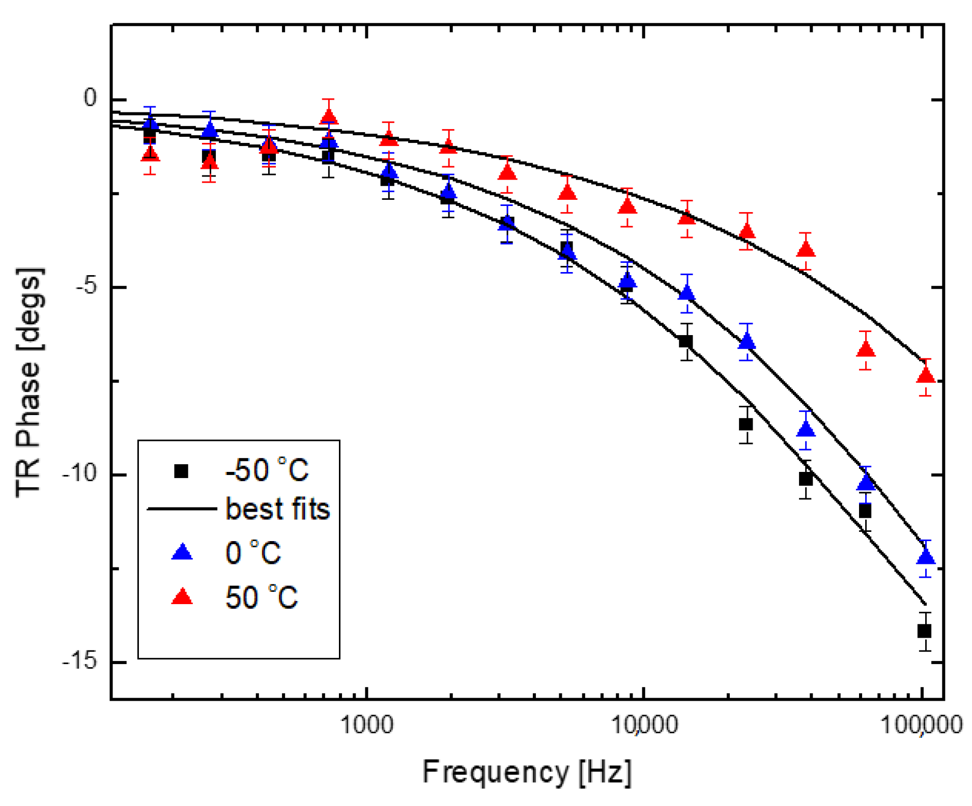
Figure 8 presents the PTR results for temperatures −50, 0 and 50 °C measured for sample #3.
The fitting procedure was identical as in our previous paper [24]. We used Matlab function lsqcurvefit for numerical calculations. First, we estimate Rth between Ti layer GaAs (sample #1). We found out that with changing temperature between −50 °C and 50 °C thermal interface boundary remains constant within the estimated error. Secondly, we use these values and data for sample #1 in estimating cross-thermal transport properties of sample #3. For the latter calculation, we used the parameters presented in Table 2.
Note that we assume that the cross-plane thermal conductivity of the gold layer and the GaAs substrate are the same thein-plane thermal conductivity at the different temperatures.
The fitting results are presented in Table 3.
The obtained results are in good agreement with the previous measurement, and some discrepancy may be due to the fact that the signal was not taken at the same location. As can be seen, all thermal transport properties decrease with increasing temperature, as expected. Only the thermal boundary resistance appears to be constant within the estimated errors. At this point, it is worth noting that the maximum observed in Figure 5 not only changes with the layer thickness (as in Figure 5 in [24]), but also with the change of the thermal transport properties. This maximum shifts to a lower frequency with increasing temperature (because the heat transport properties are deteriorated at higher temperatures).
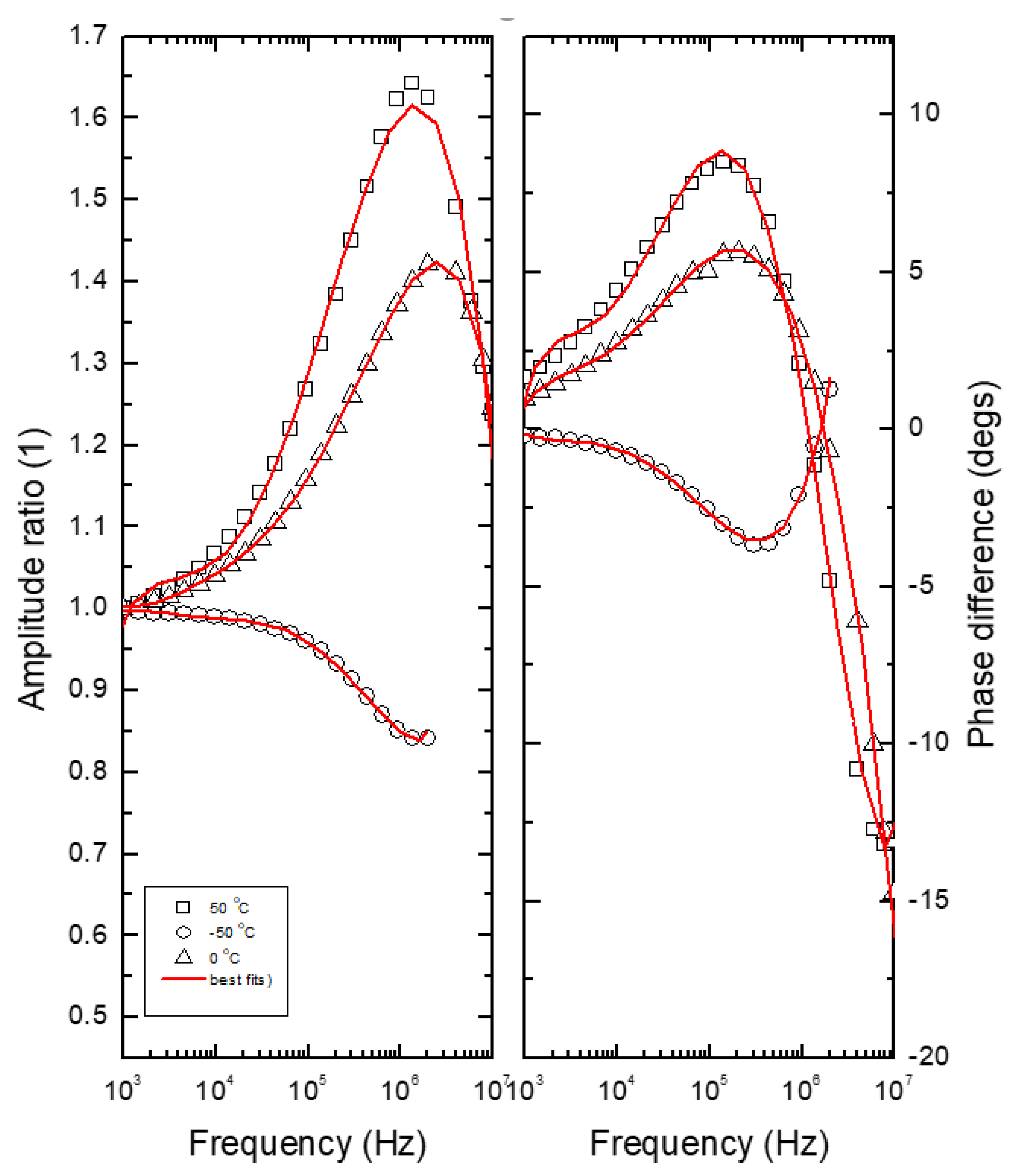
Using data presented in Table 3, the measurement of the in-plane thermal conductivity of sample #4 and the Rth between Au layer and SL layer are calculated. The obtained results are presented in Figure 9 and Table 4.
Note that the experimental results are consistent with the sensitivity analysis. The sensitivity to frequency about 1 kHz is 0, while the experimental phase to frequency of about 1 kHz is also close to 0 degs.
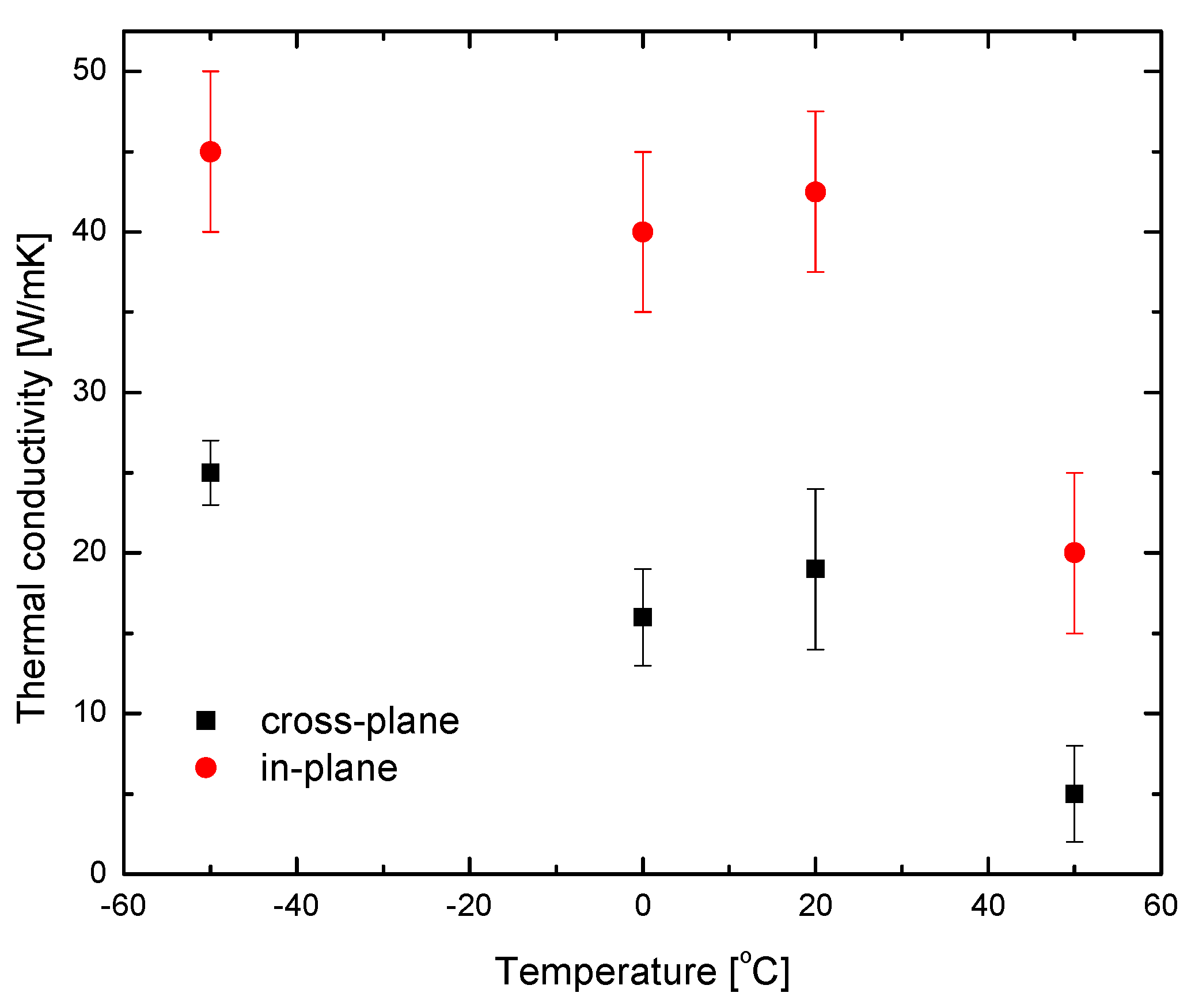
As can be seen, the in-plane thermal conductivity values are two times larger than the cross-plane thermal conductivity, as expected. The value is also consistent with those reported by authors for room temperature [36]. On the other hand, the thermal boundary resistance between gold layer and SL is within the error the same as for AlGaAs sample (sample #2). It is worth mentioning that, as with the Rth of Ti/SL layer, the thermal boundary resistance with changing temperature is constant with the estimation errors. It is also worth noting the experimental results for the same SL sample. The only difference is the metal covering the layer, but its influence is very small. Such a significant difference results from the difference in heat propagation for the one-dimensional (PTR) and three-dimensional (TR) systems.
Finally, Table 5 presents the summary in studying thermal transport properties of thin layers and superlattice using both methods frequency-domain photothermal radiometry (PTR) and frequency-domain thermoreflectance.
As one can see from Table 5, both methods complement each other rather than contend for being the most appropriate method for thermal transport parameters measurements.

5. Discussion

If we define an equivalent volumetric heat capacity ρ c eff as a weighted average of the AlAs and GaAs heat capacities, the equivalent thermal diffusivity is
α eff = k measured ( ρ c ) eff ( ρ c ) eff   ( l GaAs / l )   ρ GaAs c GaAs + ( l AlAs / l )   ρ AlAs c AlAs
where l is the superlattice period thickness.
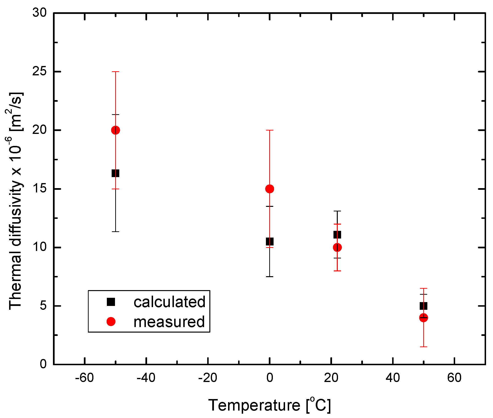
Figure 10 presents a relation between measured and calculated values of thermal diffusivity.
As can be seen in Figure 10, the measured and calculated thermal diffusivities are in good agreement. In superlattices, the in-plane thermal conductivity is two times bigger than cross-plane. Figure 11 demonstrated this relation in AlAs/GaAs superlattice sample. The thermal anisotropy of the superlattice layer confirms the expectation that the thermal conductivity is (about two times) higher in the plane than perpendicular to it which is consistent with phonon reflections at the GaAs – AlAs interfaces.
As can be observed in the figure, the tested relationship is valid for temperatures below 50 °C. In this range, the in-plane thermal conductivity is twice that of the cross-plane. For 50 °C, a slight discrepancy between the tested relationship and the obtained values can be observed, but the results are within the limits of measurement uncertainty.
Authors should discuss the results and how they can be interpreted from the perspective of previous studies and of the working hypotheses. The findings and their implications should be discussed in the broadest context possible. Future research directions may also be highlighted.

6. Conclusions

In this paper, we present the combination of two methods, FD-PTR and FD-TR, which can completely characterize the thermal properties of thin films as well as a superlattices, and experimentally verified formulas used in other studies on the thermal properties of superlattices. The results obtained are consistent with those obtained using other methods as well our previous study [21]. We found that formulas for the calculation of thermal diffusivity can be used in all studied temperature ranges. The results obtained will serve other authors to gain more confidence in the assumptions they use to calculate the specific heat of nanolayers based on their bulk material properties, perhaps in a wider temperature range.

Author Contributions

Conceptualization, M.P.; methodology, M.P., D.D.; software, M.P.; validation, M.P.; formal analysis, M.P.; investigation, M.P., N.S.; resources, A.L., T.K., A.D.W.; writing—original draft preparation, M.P.; writing—review and editing, A.L., T.K., A.D.W.; visualization, M.P.; supervision, M.P., A.D.W.; project administration, M.P.; funding acquisition, M.P., A.D.W. All authors have read and agreed to the published version of the manuscript.

Funding

This work was funded by the National Science Centre Poland grant based on Decision no. 2015/19/D/ST3/02388. A.L. and A.D.W. acknowledge the support of the DFH/UFA CDFA-05-06.

Institutional Review Board Statement

Not applicable.

Informed Consent Statement

Not applicable.

Acknowledgments

Authors would like to thank Jose Miranda-Ordonez for the help in developing the model and Nathan Jukam for discussions. We thank Nadine Viteritti for sample preparations.

Conflicts of Interest

The authors declare no conflict of interest.

References

  1. Cahill, D.G.; Goodson, K.; Majumdar, A. Thermometry and Thermal Transport in Micro/Nanoscale Solid-State Devices and Structures. J. Heat Transf. 2002, 124, 223–241. [Google Scholar] [CrossRef]
  2. Cahill, D.G. Analysis of heat flow in layered structures for time-domain thermoreflectance. Rev. Sci. Instrum. 2004, 75, 5119–5122. [Google Scholar] [CrossRef]
  3. Schmidt, A.J.; Chen, X.; Chen, G. Pulse accumulation, radial heat conduction, and anisotropic thermal conductivity in pump-probe transient thermoreflectance. Rev. Sci. Instrum. 2008, 79, 114902. [Google Scholar] [CrossRef] [PubMed] [Green Version]
  4. Hopkins, P.E.; Serrano, J.R.; Phinney, L.M.; Kearney, S.P.; Grasser, T.W.; Harris, C.T. Criteria for Cross-Plane Dominated Thermal Transport in Multilayer Thin Film Systems During Modulated Laser Heating. J. Heat Transf. 2010, 132, 081302. [Google Scholar] [CrossRef]
  5. Toberer, E.S.; Baranowski, L.L.; Dames, C. Advances in Thermal Conductivity. Annu. Rev. Mater. Res. 2012, 42, 179–209. [Google Scholar] [CrossRef]
  6. Feser, J.P.; Cahill, D.G. Probing anisotropic heat transport using time-domain thermoreflectance with offset laser spots. Rev. Sci. Instrum. 2012, 83, 104901. [Google Scholar] [CrossRef] [PubMed]
  7. Luckyanova, M.N.; Garg, J.; Esfarjani, K.; Jandl, A.; Bulsara, M.T.; Schmidt, A.J.; Minnich, A.J.; Chen, S.; Dresselhaus, M.S.; Ren, Z.; et al. Coherent Phonon Heat Conduction in Superlattices. Science 2012, 338, 936–939. [Google Scholar] [CrossRef] [Green Version]
  8. Luckyanova, M.N.; Johnson, J.A.; Maznev, A.A.; Garg, J.; Jandl, A.; Bulsara, M.T.; Fitzgerald, E.A.; Nelson, K.A.; Chen, G. Anisotropy of the Thermal Conductivity in GaAs/AlAs Superlattices. Nano Lett. 2013, 13, 3973–3977. [Google Scholar] [CrossRef] [PubMed]
  9. Favaloro, T.; Bahk, J.-H.; Shakouri, A. Characterization of the temperature dependence of the thermoreflectance coefficient for conductive thin films. Rev. Sci. Instrum. 2015, 86, 024903. [Google Scholar] [CrossRef]
  10. Cheaito, R.; Polanco, C.A.; Addamane, S.; Zhang, J.; Ghosh, A.W.; Balakrishnan, G.; Hopkins, P.E. Interplay between total thickness and period thickness in the phonon thermal conductivity of superlattices from the nanoscale to the microscale: Coherent versus incoherent phonon transport. Phys. Rev. B 2018, 97, 085306. [Google Scholar] [CrossRef] [Green Version]
  11. Jiang, P.; Huang, B.; Koh, Y.K. Accurate measurements of cross-plane thermal conductivity of thin films by dual-frequency time-domain thermoreflectance (TDTR). Rev. Sci. Instrum. 2016, 87, 075101. [Google Scholar] [CrossRef] [PubMed] [Green Version]
  12. Zevalkink, A.; Smiadak, D.M.; Blackburn, J.L.; Ferguson, A.J.; Chabinyc, M.L.; Delaire, O.; Wang, J.; Kovnir, K.; Martin, J.; Schelhas, L.T.; et al. A practical field guide to thermoelectrics: Fundamentals, synthesis, and characterization. Appl. Phys. Rev. 2018, 5, 021303. [Google Scholar] [CrossRef]
  13. Jiang, P.; Qian, X.; Yang, R. Tutorial: Time-domain thermoreflectance (TDTR) for thermal property characterization of bulk and thin film materials. J. Appl. Phys. 2018, 124, 161103. [Google Scholar] [CrossRef] [Green Version]
  14. Koh, Y.K.; Singer, S.L.; Kim, W.; Zide, J.M.; Lu, H.; Cahill, D.G.; Majumdar, A.; Gossard, A.C. Comparison of the 3ω method and time-domain thermoreflectance for measurements of the cross-plane thermal conductivity of epitaxial semiconductors. J. Appl. Phys. 2009, 105, 054303. [Google Scholar] [CrossRef]
  15. Chávez, E.; Cuffe, J.; Alzina, F.; Torres, C.S. Calculation of the specific heat in ultra-thin free-standing silicon membranes. J. Phys. 2012, 395, 012105. [Google Scholar] [CrossRef]
  16. Markushev, D.K.; Markushev, D.D.; Aleksic, S.M.; Pantic, D.S.; Galovic, S.P.; Todorovic, D.M.; Ordonez-Miranda, J. Effects of the photogenerated excess carriers on the thermal and elastic properties of n-type silicon excited with a modulated light source: Theoretical analysis. J. Appl. Phys. 2019, 126, 185102. [Google Scholar] [CrossRef]
  17. Markushev, D.K.; Markushev, D.D.; Aleksic, S.M.; Pantic, D.S.; Galovic, S.P.; Todorovic, D.M.; Ordonez-Miranda, J. Experimental photoacoustic observation of the photogenerated excess carrier influence on the thermoelastic response of n-type silicon. J. Appl. Phys. 2020, 128, 095103. [Google Scholar] [CrossRef]
  18. Korte, D.; Cabrera, H.; Toro, G.; Grima, J.; Leal, C.; Villabona, A.; Franko, M. Optimized frequency dependent photothermal beam deflection spectroscopy. Laser Phys. Lett. 2016, 13, 1–12. [Google Scholar] [CrossRef] [Green Version]
  19. Korte, D.; Pavlica, E.; Bratina, G.; Franko, M. Characterization of pure and modified TiO2 layer on glass and aluminium support by beam deflection spectrometry. Int. J. Thermophys. 2014, 35, 1990–2000. [Google Scholar] [CrossRef]
  20. Cabrera, H.; Matroodi, F.; Cabrera-Díaz, H.D.; Ramírez-Miquet, E.E. Frequency-resolved photothermal lens: An alternative approach for thermal diffusivity measurements in weak absorbing thin samples. Int. J. Heat Mass Transf. 2020, 158, 120036. [Google Scholar] [CrossRef]
  21. Cabrera, H.; Ramírez-Miquet, E.E.; Suarez-Vargas, J.J.; Ramírez, J.F.; Korte, D.; Niemela, J.J. Pump-Probe Photothermal Self-Mixing System for Highly Sensitive Trace Detection. IEEE Sens. J. 2019, 19, 2547–2552. [Google Scholar] [CrossRef]
  22. Schmidt, A.J.; Cheaito, R.; Chiesa, M. A frequency-domain thermoreflectance method for the characterization of thermal properties. Rev. Sci. Instrum. 2009, 80, 094901. [Google Scholar] [CrossRef] [PubMed]
  23. Zhu, J.; Tang, D.; Wang, W.; Liu, J.; Holub, K.W.; Yang, R. Ultrafast thermoreflectance techniques for measuring thermal conductivity and interface thermal conductance of thin films. J. Appl. Phys. 2010, 108, 094315. [Google Scholar] [CrossRef]
  24. Pawlak, M.; Jukam, N.; Kruck, T.; Dziczek, D.; Ludwig, A.; Wieck, A.D. Measurement of thermal transport properties of selected superlattice and thin films using frequency-domain photothermal infrared radiometry. Measurement 2020, 166, 108226. [Google Scholar] [CrossRef]
  25. Trefon-Radziejewska, D.; Juszczyk, J.; Fleming, A.; Horny, N.; Antoniow, J.S.; Chirtoc, M.; Kaźmierczak-Bałata, A.; Bodzenta, J. Thermal characterization of metal phthalocyanine layers using photothermal radiometry and scanning thermal microscopy methods. Synth. Met. 2017, 232, 72–78. [Google Scholar] [CrossRef]
  26. Trefon-Radziejewska, D.; Hamaoui, G.; Chirtoc, M.; Horny, N.; Smokal, V.; Biitseva, A.; Krupka, O.; Derkowska-Zielinska, B. Thermal properties of methacrylic polymer films with guest-host and side-chain azobenzene. Mater. Chem. Phys. 2019, 223, 700–707. [Google Scholar]
  27. Fuente, R.; Apiñaniz, E.; Mendioroz, A. Agustín Salazar Simultaneous measurement of thermal diffusivity and optical absorption coefficient using photothermal radiometry. I. Homog. Solids 2011, 110, 033515. [Google Scholar]
  28. Nordal, P.; Kanstad, S. Photothermal Radiometry. Phys. Scr. 1979, 20, 659–662. [Google Scholar] [CrossRef]
  29. Pawlak, M.; Pal, S.; Scholz, S.; Ludwig, A.; Wieck, A.D. Simultaneous measurement of thermal conductivity and diffusivity of an undoped Al0.33Ga0.67As thin film epitaxially grown on a heavily Zn doped GaAs using spectrally-resolved modulated photothermal infrared radiometry. Thermochim. Acta 2018, 662, 69–74. [Google Scholar] [CrossRef]
  30. Pawlak, M.; Horny, N.; Scholz, S.; Ebler, C.; Ludwig, A.; Wieck, D.A. Simultaneous measurement of infrared absorption coefficient of Carbon doped Al0.33Ga0.67As thin film and thermal boundary resistance between thin film and heavily Zn doped GaAs using spectrally-resolved modulated photothermal infrared radiometry. Thermochim. Acta 2018, 667, 73–78. [Google Scholar] [CrossRef]
  31. Malinski, M.; Chrobak, L. Investigations and modeling aspects of the influence of the high energy and high dose implantation on the optical and transport parameters of implanted layers in silicon. Phys. B Condens. Matter 2020, 578, 411851. [Google Scholar] [CrossRef]
  32. Dorywalski, K.; Chrobak, L.; Malinski, M. Comparative Studies of The Optical Absorption Coefficient Spectra in The Implanted Layers in Silicon with The Use of Nondestructive Spectroscopic Techniques. Metrol. Meas. Syst. 2020, 27, 323–337. [Google Scholar]
  33. Jiang, P.; Qian, X.; Yang, R. A new elliptical-beam method based on time-domain thermoreflectance (TDTR) to measure the in-plane anisotropic thermal conductivity and its comparison with the beam-offset method. Rev. Sci. Instrum. 2018, 89, 09490. [Google Scholar] [CrossRef]
  34. el Helou, A.; Raad, P.E.; Komarov, P. Temperature dependence of the thermoreflectance coefficient of gold by the use of a phase-locked single-point measurement approach. In Proceedings of the 2018 34th Thermal Measurement, Modeling & Management Symposium (SEMI-THERM), San Jose, CA, USA, 19–23 March 2018; pp. 161–164. [Google Scholar]
  35. Adachi, S. GaAs, AlAs, and AlxGa1-xAs: Material parameters for use in research and device applications. J. Appl. Phys. 1985, 58, R1. [Google Scholar] [CrossRef]
  36. Cardenas, C.; Fabris, D.; Tokairin, S.; Madriz, F.; Yang, C.Y. Thermoreflectance Measurement of Temperature and Thermal Resistance of Thin Film Gold. J. Heat Transf. 2012, 134, 111401. [Google Scholar] [CrossRef]
  37. Mei, S.; Knezevic, I. Thermal conductivity of III-V semiconductor superlattices. J. Appl. Phys. 2015, 118, 175101. [Google Scholar] [CrossRef] [Green Version]
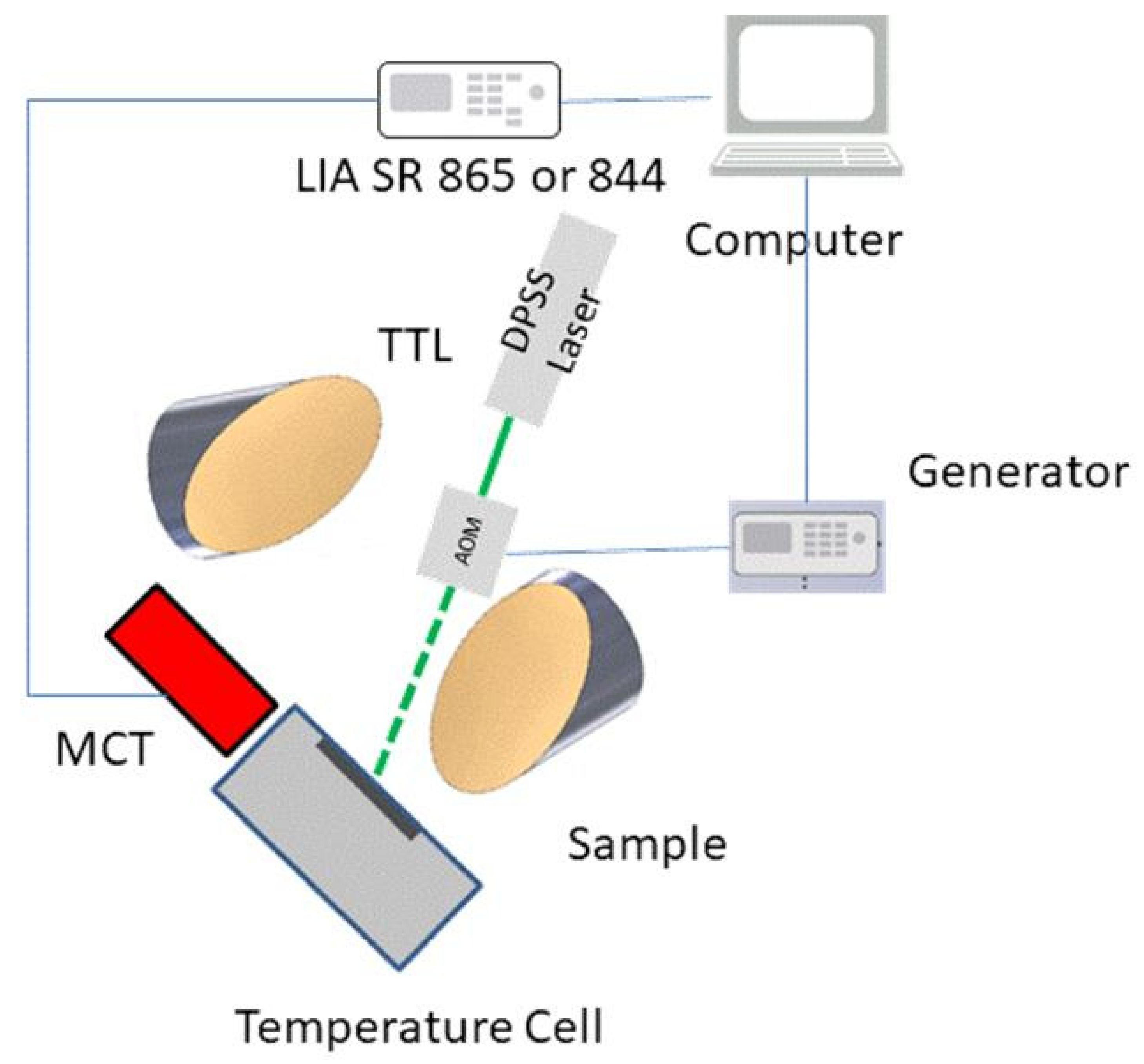
Figure 1. Frequency-domain photothermal infrared radiometry set-up with temperature cell. The beam size was 1.8 mm.
Applsci 11 06125 g001
Figure 2. Temperature-dependent of the PTR and TR amplitudes at 1 kHz for a GaAs wafer covered by 50 layer of Ti and 2 µm AlGaAs thin layer with 100 nm of gold layer, respectively. The data are not normalized. The signals were depicted for 1 kHz. Note that PTR amplitude is very stable with error bars within experimental points.
Applsci 11 06125 g002
Figure 3. FD-TR setup.
Applsci 11 06125 g003
Figure 4. SEM image of superlattice sample (samples #3 and #4).
Applsci 11 06125 g004
Figure 5. Cross-plane (left) and in-plane (right) geometry in frequency-domain methods.
Applsci 11 06125 g005
Figure 6. Phase relative sensitivities of model described by Equation (1) to the parameters (RAlGaAs/GaAs = 1.0 × 10⁻⁹ m2 2 K/W, kAlGaAs = 12 W/mK, αAlGaAs=6 × 10⁻⁶ m2 /s, L = 500 nm) and with other parameter values taken from Table 2.
Applsci 11 06125 g006
Figure 7. Measured TR phase of 2 µm AlGaAs thin layer covered by 100 nm of gold layer between 100 Hz and 500 kHz. The best fits are obtained using Equation (1).
Applsci 11 06125 g007
Figure 8. PTR experimental results (points) for sample#3 in three different temperatures: −50 °C, 0 °C and 50 °C. Additionally, the best fittings are presented as solid lines using Equation (8).
Applsci 11 06125 g008
Figure 9. TR measurement of sample #4 for different temperatures. Experimental points are circles, while fits are lines. The red (50 °C), black (−50 °C) and blue (0 °C). The best fits are obtained using Equation (1).
Applsci 11 06125 g009
Figure 10. Relation between measured and calculated values of thermal diffusivity as function of temperature.
Applsci 11 06125 g010
Figure 11. Relation between in-plane and cross-plane thermal conductivity measured for AlAs/GaAs superlattice sample as function of temperature.
Applsci 11 06125 g011
Table 1. Summary of the sample properties.
Thicknesses Estimated from Reflectivity Measurement [24]DescriptionMetalic Layer on the Top
Sample #1-Undoped GaAs used as substrate;Ti 50 nm
Sample #21980 nmThin Al0.33Ga0.67As alloyAu 100 nm
Sample #3520 nmAlAs/GaAs superlattice with period thickness of 52 nmTi 50 nm
Sample #4520 nmAlAs/GaAs superlattice with period thickness of 52 nmAu 100 nm
Table 2. Constant parameters used for calculation.
ParameterThree Layer
k1 = kTi (W/mK) at −50 °C22.9
k1 = kTi (W/mK) at 0 °C21.5
k1 = kTi (W/mK) at 50 °C21.0
α1 = αTi (m2/s) for all temperatures8 × 10−6
k1 = kau (W/mK) at −50 °C321
k1 = kAu (W/mK) at 0 °C318
k1 = kAu (W/mK) at 50 °C315
α1 = αAu (m2/s) for all temperatures127 × 10−6
RTi/GaAs (R12)2.0 × 10⁻⁸ (m2 KW−1) from reference measurement
k3 = kGaAs (W/mK) at −50 °C70
α3 = αGaAs (m2/s) at −50 °C4.2 × 10−5
k3 = kGaAs (W/mK) at 0 °C60
α3 = αGaAs (m2/s) at 0 °C3.2 × 10−5
k3 = kGaAs (W/mK) at 50 °C30
α3 = αGaAs (m2/s) at 50 °C1.7 × 10−5
Table 3. Cross-plane thermal transport parameters of the AlAs/GaAs superlattice, obtained from fits to the PTR data in Figure 5 for different temperatures.
Temperature (°C)kGaAs/AlAs (W/mK)αGaAs/AlAs (m2/s)Rth,23 (m2KW−1)
−5025 ± 2(2.0 ± 0.6) × 10−5(2 ± 0.2) × 10−8
016 ± 3(1.5 ± 0.5) × 10−5(1 ± 0.5) × 10−8
508 ± 3(4.0 ± 2.5) × 10−6(1.5 ± 0.9) × 10−8
RT [15]19 ± 5(1.0 ± 0.2) × 10−5(3.0 ± 0.8) × 10−8
Table 4. In-plane thermal transport parameters of AlAs/GaAs superlattice obtained from fits to the PTR data in Figure 5 for different temperatures.
Temperature (°C)kGaAs/AlAs (W/mK)Rth,12 (m2KW−1)
−5045 ± 5(0.9 ± 0.2) × 10−7
040 ± 5(1 ± 0.9) × 10−7
5020 ± 5(1.5 ± 0.9) × 10−7
Table 5. The summary of frequency-domain photothermal radiometry (PTR) and frequency-domain thermoreflectance.
FeatureFrequency Domain PTRFrequency Domain TR
AdvantagesDisadvantageAdvantagesDisadvantage
Measurement of cross-plane thermal transport propertiesPossible Difficult but possible
Measurement of in-plane thermal transport properties Difficult but possiblePossible
Complexity of optical systemRelatively easy Relatively difficult
Temperature-measurements at low temperaturesDifficult Possible
Temperature measurements at high temperaturesPossible Possible
Publisher’s Note: MDPI stays neutral with regard to jurisdictional claims in published maps and institutional affiliations.