Featured Application
This study allows power converters to achieve high conversion efficiency due to the low parasitic inductance of multi-chip integration technology.
Abstract
Half-bridge modules with integrated GaN high electron mobility transistors (HEMTs) and driver dies were designed and fabricated in this research. Our design uses flip-chip technology for fabrication, instead of more generally applied wire bonding, to reduce parasitic inductance in both the driver-gate and drain-source loops. Modules were prepared using both methods and the double-pulse test was applied to evaluate and compare their switching characteristics. The gate voltage () waveform of the flip-chip module showed no overshoot during the turn-on period, and a small oscillation during the turn-off period. The probabilities of gate damage and false turn-on were greatly reduced. The inductance in the drain-source loop of the module was measured to be 3.4 nH. The rise and fall times of the drain voltage () were 12.9 and 5.8 ns, respectively, with an overshoot of only 4.8 V during the turn-off period under = 100 V. These results indicate that the use of flip-chip technology along with the integration of GaN HEMTs with driver dies can effectively reduce the parasitic inductance and improve the switching performance of GaN half-bridge modules compared to wire bonding.
1. Introduction
In recent years, GaN high electron mobility transistors (HEMTs) have been widely applied in power electronic converters to improve power density and efficiency, even under harsh operating environments, thanks to their high breakdown voltage, low on-resistance, high switching speed, and high temperature capability [1,2,3,4]. However, the high switching speed of GaN HEMT results in a large and , which causes overshoot and oscillation in the gate voltage (), drain voltage ), and current () because of parasitic inductance in the driver and power loops [5,6].
To reduce parasitic inductance, new packaging methods have been reported, such as optimized printed circuit board (PCB) layouts [7,8], the optimized interconnection method [9], hybrid packaging [10,11], and integrating driver chips into modules [12,13]. Despite reduced parasitic inductance, the drivers used were all packaged chips. To further reduce the inductance between the driver chip output terminal and the GaN HEMT gate, as well as the inductance in driver grounding, drivers and GaN HEMT dies were integrated into an 8.00 × 8.00 mm quad flat no-leads (QFN) package by Texas Instruments Incorporated [14]. On the other hand, it was shown that flip-chip technology can further reduce the parasitic inductance and make modules more compact than general wire bonding [15,16].
In this paper, a GaN half-bridge module integrated with HEMTs and driver dies was fabricated using flip-chip technology. The parasitic inductance of the power loop was extracted as 3.4 nH. The switching characteristics of the module were evaluated by a double-pulse test and compared with that of a module that was packaged using the wire bonding process. The waveform of the flip-chip module showed no overshoot at the turn-on period and a small oscillation at the turn-off period, indicating that this method effectively reduced the probability of gate damage and false turn-on. In addition, the waveform of the flip-chip module was flat, with almost no overshoot and oscillation. The fall and rise times of were 12.9 and 5.8 ns, respectively. These results indicate that an integrated module with dies created using flip-chip technology can obtain superior switching characteristics.
2. Module Design and Fabrication
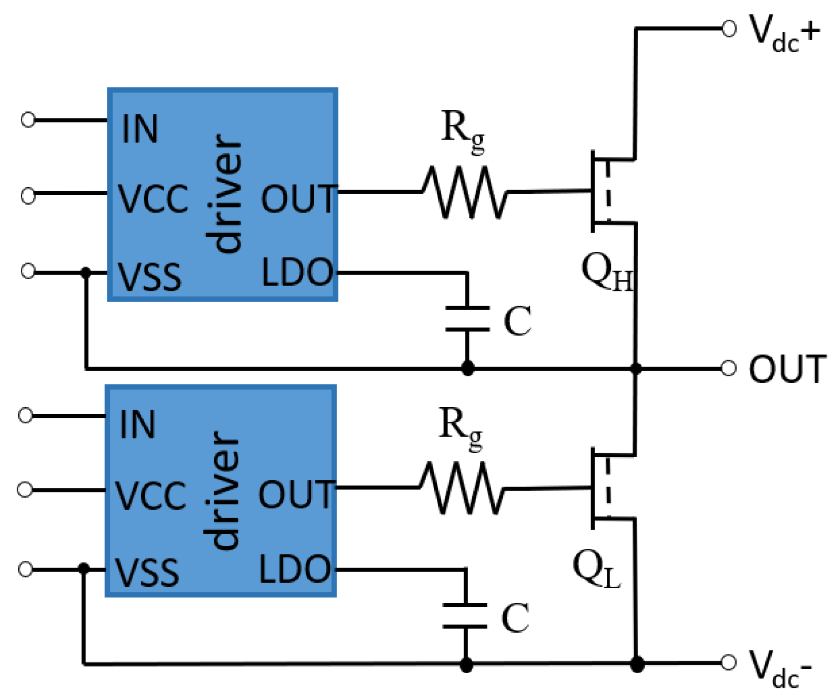
The equivalent circuit diagram of the integrated GaN half-bridge module is shown in Figure 1. Every driver loop includes a driver die, 1 Ω resistor, and 1 μF capacitor. The power loop of the module consists of GaN enhancement-mode (e-mode) HEMTs with a threshold voltage () of 1 V, breakdown voltage (BV) of 650 V, and on-resistance (Ron) of 100 mΩ. The module uses AlN as the substrate material for decent heat dissipation performance.

Figure 1.
Schematic of the integrated GaN half-bridge module.
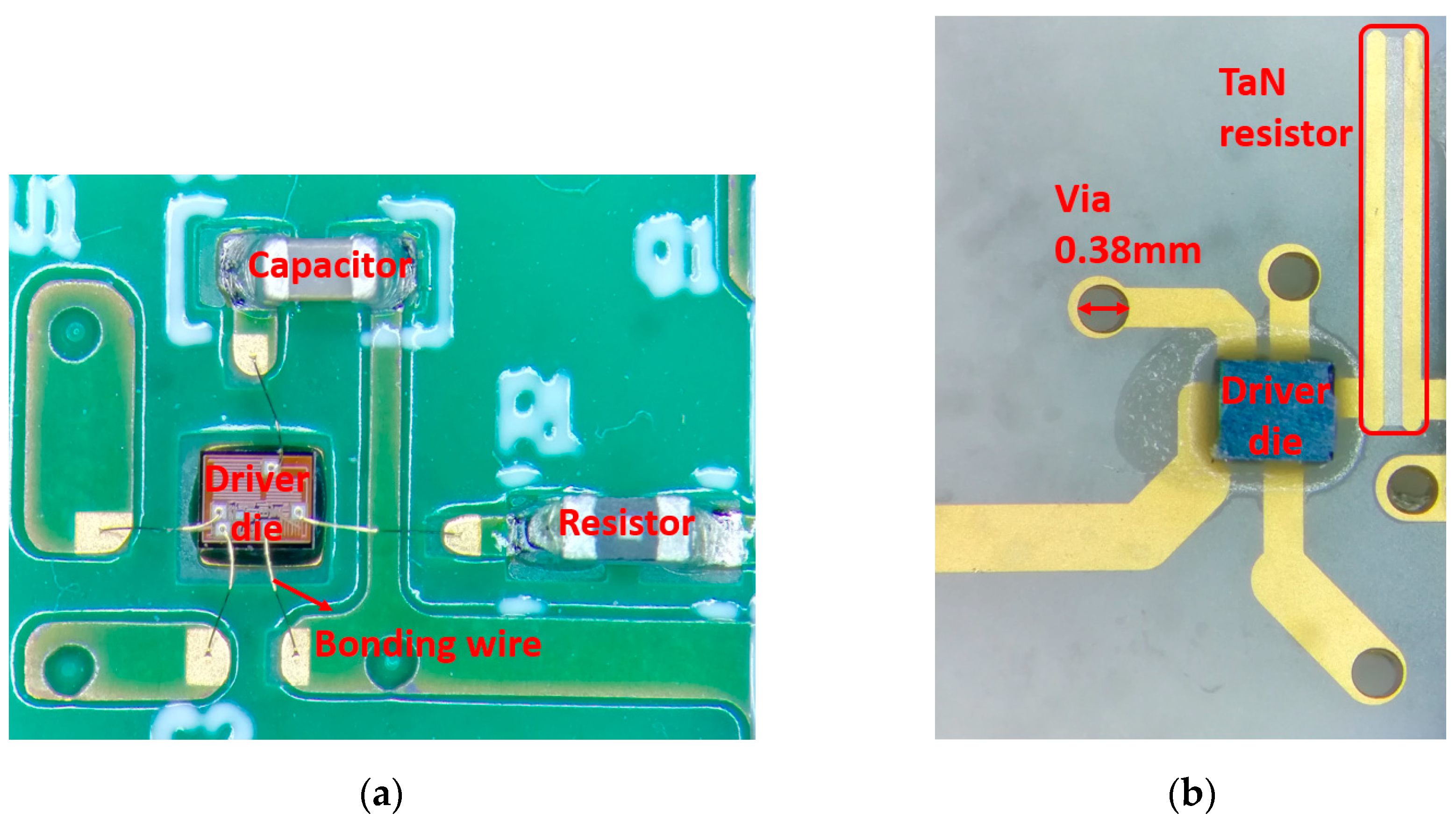
To reduce the trace length of the driver loop and obtain lower inductance, two modules were fabricated with integrated driver dies. The difference between these two modules is that the driver loops of the two modules were packaged either by the wire bonding process or using flip-chip technology. A microscope photograph of the driver loop packaged by wire bonding is shown in Figure 2a. The diameter of the bonding Au wire was 20 μm. The capacitor and resistor were interconnected with the substrate by surface mount technology (SMT) in this module. The distance between the out terminal of the driver and the gate of the HEMT device was more than 4 mm. As shown in Figure 2b, the driver die in the other module was packaged by flip-chip technology through gold balls. The diameter of the gold balls was approximately 60 μm. A capacitor was set on the reverse side of the substrate by SMT, and a tantalum nitride (TaN) film was used as the gate resistor on the substrate. The distance between the out terminal of the driver and the gate of the HEMT was as short as 1.3 mm.

Figure 2.
Microscope photograph of the driver loop (a) packaged by wire bonding technology; (b) packaged by flip-chip technology.
A microscope photograph of the power loop is shown in Figure 3. In order to reduce the parasitic inductance of the power loop, the HEMTs were packaged in the module by flip-chip technology. There were 36 gold balls on the source and drain pads, and two gold balls on the gate pad. The parasitic inductance of the power loop was extracted using an Agilent E4980A Precision LCR Meter, which was measured as 3.4 nH. This shows that the module integration achieved ultra-small parasitic inductance of the power loop.
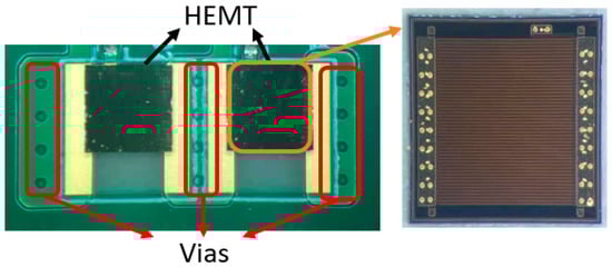
Figure 3.
Microscope photograph of the power loop and the golden ball distribution of the HEMT.
3. Switching Characteristics
The switching characteristics of the modules were evaluated using a double-pulse test circuit with a load inductor of 600 μH. In the test, the high-side input logic signal was kept at zero to ensure the high-side HEMT was used as a freewheeling channel, while the double-pulse signal was applied on the low-side HEMT. The and of the low-side HEMT were measured using a Tektronix MSO64B oscilloscope.
The waveforms of these two modules are shown in Figure 4. During the turn-on period, as the input of was 6 V, the overshoot of in the wire-bonding module was 1.24 V, while there was almost no overshoot in the module in the flip-chip package. In addition, there was strong oscillation in the wire-bonding module in the turn-off period, whose maximum amplitude was about 1.24 V. This is higher than the of the HEMT (1 V), meaning that there might be false turn-on operations in the wire-bonding module. The rise time of was 13.5 and 12.5 ns for the flip-chip and wire bonding modules, respectively. The fall time of was 10.0 and 9.1 ns for the flip-chip and wire bonding modules, respectively. These findings indicate that the parasitic inductance of the driver loop was effectively reduced by the application of flip-chip technology.
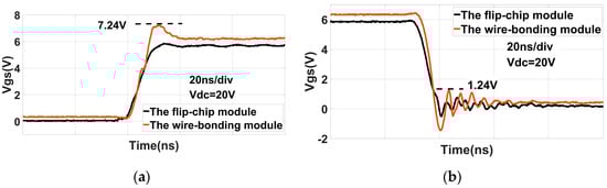
Figure 4.
Gate-source voltage waveforms of the modules prepared by different processes under : (a) turn-on period; (b) turn-off period.
The waveforms of the flip-chip module under a of 100 V are shown in Figure 5. The test was carried out under 100 V because the module had no additional insulation protection and heat sink. The fall time of was 5.8 ns, which corresponds to a dv/dt of 17.2 V/ns during the turn-on period. The rise time of was 12.9 ns for the module, with a dv/dt of 7.8 V/ns during the turn-off period. The waveform of the integrated module was stable after a small overshoot of 4.8 V during the turn-off period.
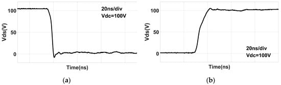
Figure 5.
Drain-source voltage waveforms of the integrated module under : (a) turn-on period; (b) turn-off period.
To illustrate the advantages of the flip-chip technology, the test results of the integrated module were compared with that of [8], whose circuit structure is similar to this work. In reference [8], a GaN half-bridge module was fabricated with integrated drivers by the wire bonding process. Under the same test conditions of 100V/2.7A, the overshoot of of the module in [8] was approximately 25V, which is four times larger than the result of this work. During the turn-off period, the current decreased gradually. Due to the existence of parasitic inductance in the power loop, a voltage in phase with was induced on it, which manifested as overshoot of . This means that the parasitic inductance of power loop in reference [8] is larger than this work, which indicates advantages of the flip-chip technology.
4. Conclusions
We designed and fabricated a half-bridge module whose gate driver dies were closely integrated with the power devices. Both the HEMTs and driver dies were flip-chip bonded onto the AlN substrate without bonding wires. The parasitic inductance of the power loop for the module was measured to be 3.4 nH. The switching performance of the module was evaluated using the double-pulse test. The module showed an ultrasmall overshoot and oscillation in the waveform as well as a high switching speed in the . The rise and fall times of the module were measured to be 5.8 and 12.9 ns, respectively. Compared with a module packaged by the wire bonding process, the flip-chip module had reduced trace length and achieved lower parasitic inductance, showing excellent switching characteristics. This work is encouraging for the realization of an integration module with low parasitic inductance and excellent switching performance.
Author Contributions
Methodology, L.W., D.-F.L. and Y.Z.; investigation, L.W. and Z.-G.Y.; validation, L.W. and Z.C.; data curation, L.W. and L.-F.J.; writing—original draft preparation, L.W.; writing—review and editing, Y.Z.; project administration, Z.L. and Y.Z. All authors have read and agreed to the published version of the manuscript.
Funding
This research was funded by the National Key Research and Development Program of China under Grant No. 2017YFB0402903, the Science Challenge Project under Grant TZ2018003, and the National Natural Science Foundation of China under Grant 61874114, 61674143 and 61974137.
Acknowledgments
The authors would like to express their appreciation for Xiamen Sanan Integrated Circuit Co., Ltd. and Qin-Song Qian of Southeast University for providing the HEMTs and driver dies, respectively.
Conflicts of Interest
The authors declare no conflict of interest.
References
- Niloufar, K.; Deqiang, W.; Bharat, A.; Ruoyu, H.; Ali, E. Current Status and Future Trends of GaN HEMTs in Electrified Transportation. IEEE Access 2020, 8, 70553–70571. [Google Scholar]
- Joshin, K.; Kikkawa, T.; Masuda, S.; Watanabe, K. Outlook for GaN HEMT Technology. Fujitsu Sci. Tech. J. 2014, 50, 138–143. [Google Scholar]
- Fletcher, A.S.A.; Nirmal, D. A survey of Gallium Nitride HEMT for RF and high power applications. Superlattices Microstruct. 2017, 109, 519–537. [Google Scholar] [CrossRef]
- De Santi, C.; Meneghini, M.; Meneghesso, G.; Zanoni, E. Review of dynamic effects and reliability of depletion and enhancement GaN HEMTs for power switching applications. Iet Power Electron. 2018, 11, 668–674. [Google Scholar] [CrossRef]
- Luo, F.; Liang, L.; Huitink, D.; Spiesshoefer, S. Advanced Power Module Packaging and Integration Structures for High Frequency Power Conversion: From Silicon to GaN. Power Electron. 2018, 52, 9–18. [Google Scholar]
- Lautner, J.; Piepenbreier, B. Analysis of GaN HEMT Switching Behavior. In Proceedings of the 2015 9th International Conference on Power Electronics and Ecce Asia, Seoul, Korea, 1–5 June 2015; pp. 567–574. [Google Scholar]
- Reusch, D.; Strydom, J. Understanding the Effect of PCB Layout on Circuit Performance in a High-Frequency Gallium-Nitride-Based Point of Load Converter. IEEE Trans. Power Electron. 2014, 29, 2008–2015. [Google Scholar] [CrossRef]
- Kuring, C.; Wolf, M.; Geng, X.; Hilt, O.; Bocker, J.; Wieczorek, N.; Wurfl, J.; Dieckerhoff, S. Evaluation of a GaN HEMT Half-Bridge embedded to a Multilayer Aluminum Nitride Substrate. In Proceedings of the CIPS 2020; 11th International Conference on Integrated Power Electronics Systems. VDE, Berlin, Germany, 24–26 March 2020; pp. 1–6. [Google Scholar]
- Liu, W.; Mei, Y.; Xie, Y.; Wang, M.; Li, X.; Lu, G.-Q. Design and Characterizations of a Planar Multichip Half-Bridge Power Module by Pressureless Sintering of Nanosilver Paste. IEEE J. Emerg. Sel. Top. Power Electron. 2019, 7, 1627–1636. [Google Scholar] [CrossRef]
- Chen, C.; Chen, Y.; Li, Y.; Huang, Z.; Liu, T.; Kang, Y. An SiC-Based Half-Bridge Module with an Improved Hybrid Packaging Method for High Power Density Applications. IEEE Trans. Ind. Electron. 2017, 64, 8980–8991. [Google Scholar] [CrossRef]
- Chen, C.; Huang, Z.; Chen, L.; Tan, Y.; Kang, Y.; Luo, F. Flexible PCB-Based 3-D Integrated SiC Half-Bridge Power Module With Three-Sided Cooling Using Ultralow Inductive Hybrid Packaging Structure. IEEE Trans. Power Electron. 2019, 34, 5579–5593. [Google Scholar] [CrossRef]
- Guo, S.; Zhang, L.; Lei, Y.; Li, X.; Xue, F.; Yu, W.; Huang, A.Q. 3.38 Mhz Operation of 1.2kV SiC MOSFET With Integrated Ultra-Fast Gate Drive. In Proceedings of the Wipda 2015 3rd Ieee Workshop on Wide Bandgap Power Devices and Applications, Blacksburg, VA, USA, 2–4 November 2015; pp. 390–395. [Google Scholar]
- Zhao, X.; Gao, B.; Zhang, L.; Hopkins, D.C.; Huang, A.Q. Performance Optimization of A 1.2kV SiC High Density Half Bridge Power Module in 3D Package. In Proceedings of the Thirty-Third Annual Ieee Applied Power Electronics Conference and Exposition, San Antonio, TX, USA, 4–8 March 2018; pp. 1266–1271. [Google Scholar]
- Chen, J.; Xie, Y.; Trombley, D.; Murugan, R. System Co-design of a 600V GaN FET Power Stage with Integrated Driver in a QFN System-in-Package (QFN-SiP). In Proceedings of the 2019 IEEE 69th Electronic Components and Technology Conference (ECTC), Las Vegas, NV, USA, 28–31 May 2019; pp. 1221–1226. [Google Scholar]
- Seal, S.; Wallace, A.K.; Dearien, A.M.; Farnell, C.; Mantooth, H.A. A Wire Bondless SiC Switching Cell With a Vertically Integrated Gate Driver. IEEE Trans. Power Electron. 2020, 35, 9690–9699. [Google Scholar] [CrossRef]
- Seal, S.; Glover, M.D.; Mantooth, H.A. 3-D Wire Bondless Switching Cell Using Flip-Chip-Bonded Silicon Carbide Power Devices. IEEE Trans. Power Electron. 2018, 33, 8553–8564. [Google Scholar] [CrossRef]


Publisher’s Note: MDPI stays neutral with regard to jurisdictional claims in published maps and institutional affiliations. |
© 2021 by the authors. Licensee MDPI, Basel, Switzerland. This article is an open access article distributed under the terms and conditions of the Creative Commons Attribution (CC BY) license (https://creativecommons.org/licenses/by/4.0/).