
Assessment of Manufacturing Parameters for New 3D-Printed Heating Circuits Based on CNT-Doped Nanocomposites Processed by UV-Assisted Direct Write

 ,
,  ,
,  ,
,  and
and 
Abstract
:1. Introduction
2. Materials and Methods
2.1. Materials
2.2. 3D Printing of Electrically Conductive Circuits
2.3. Characterization
2.3.1. Optimization of 3D-Printing Method
2.3.2. Electrical Conductivity
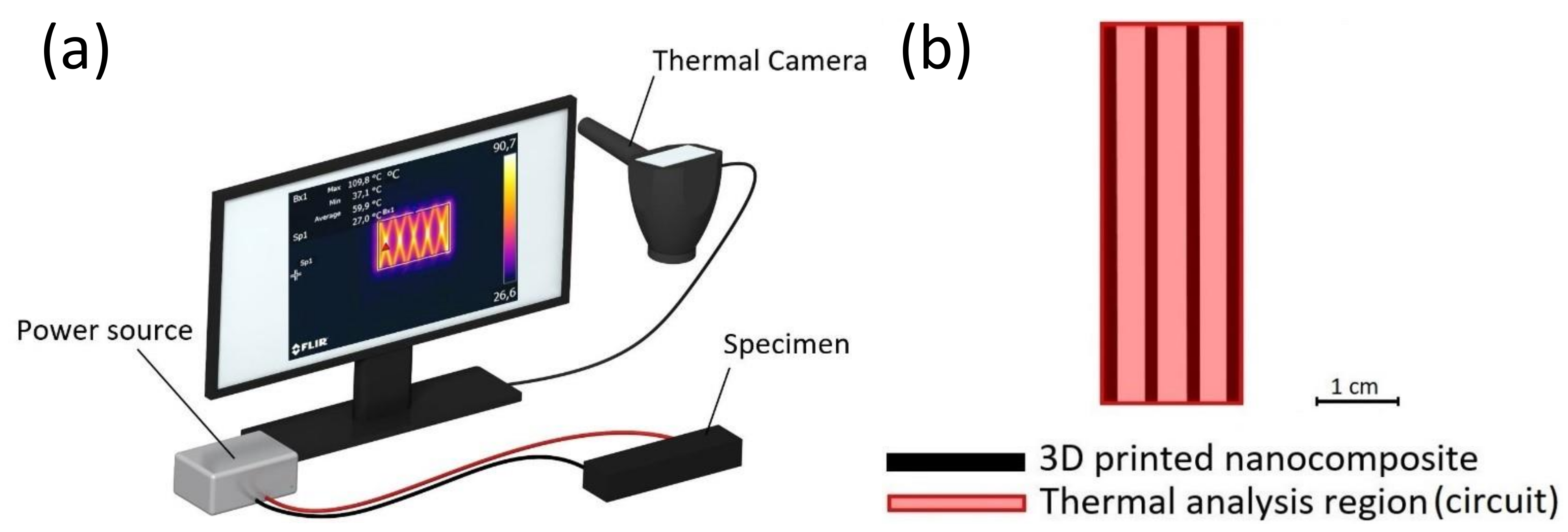
2.3.3. Self-Heating by Joule’s Effect
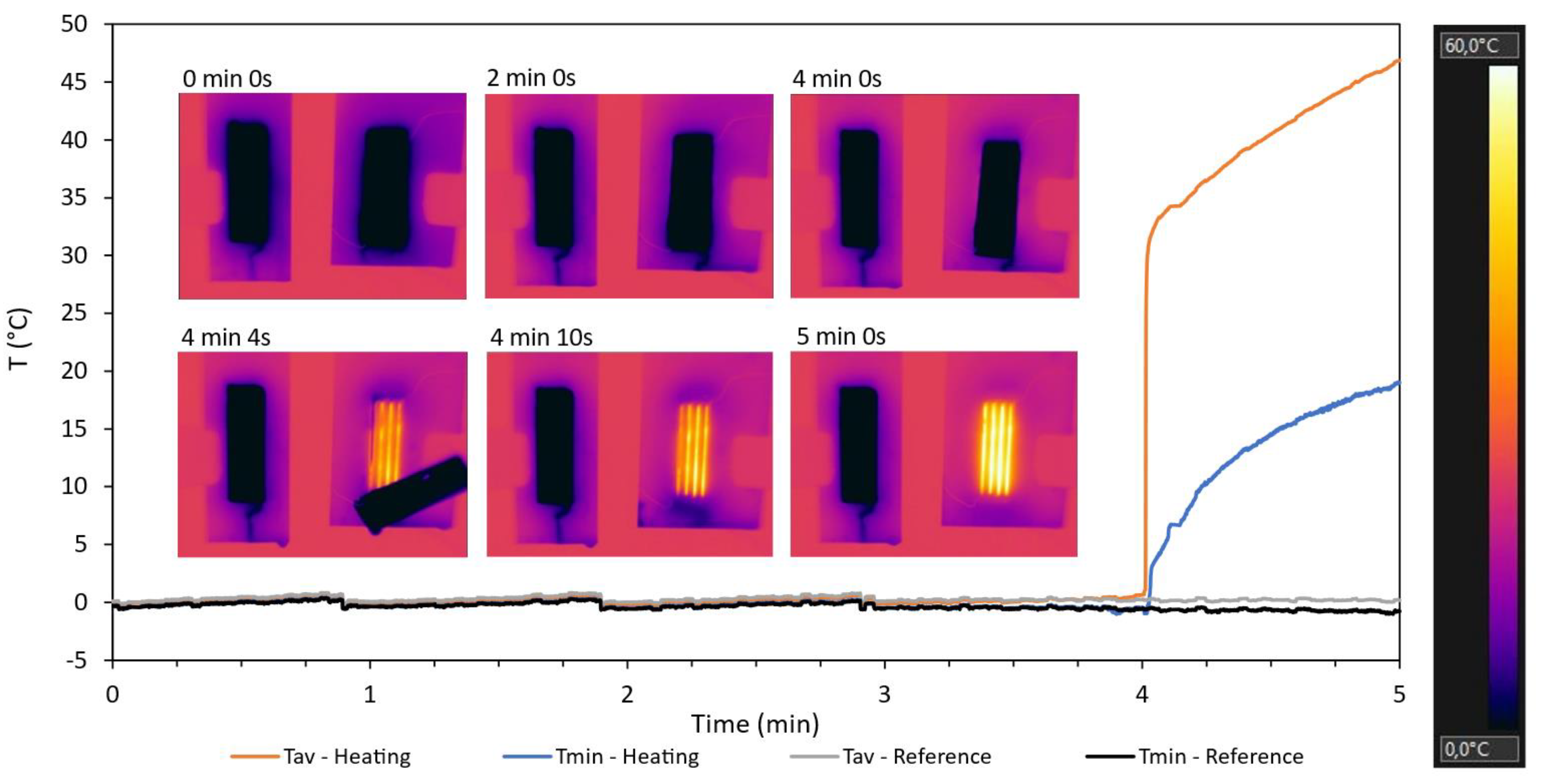
2.3.4. Deicing Test
3. Results and Discussion
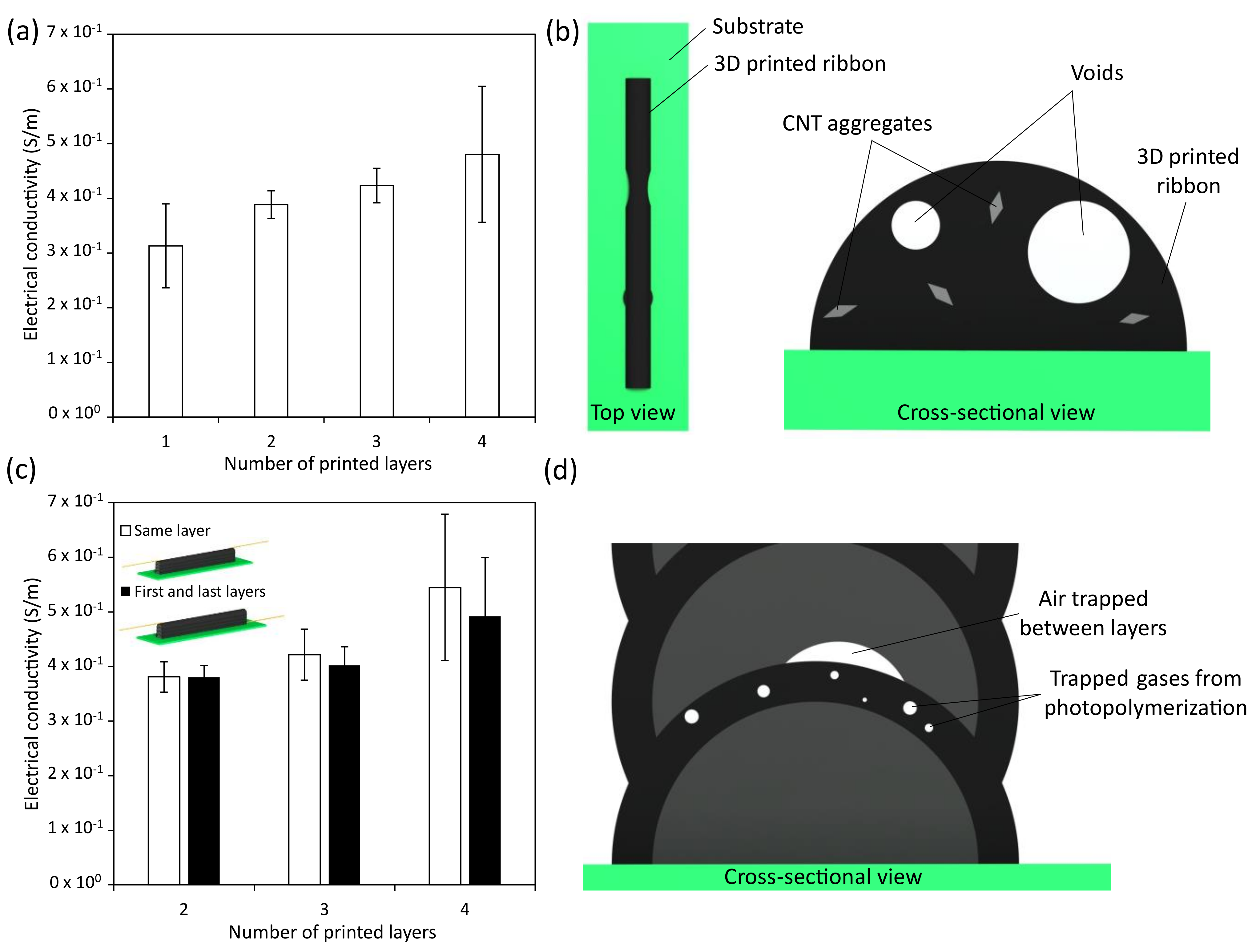
3.1. Study of 3D Printing Quality
3.2. Electrical Conductivity
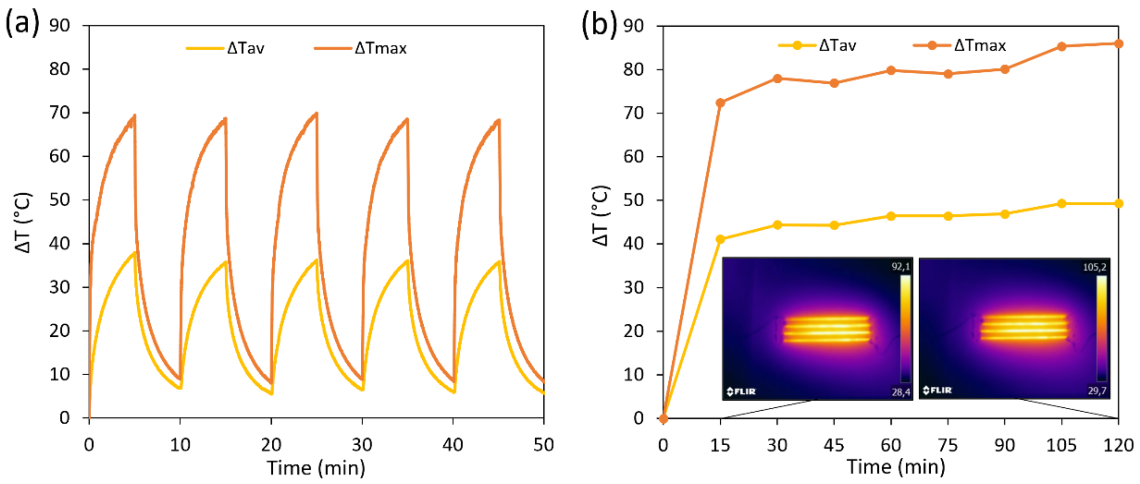
3.3. Self-Heating by Joule’s Effect
4. Conclusions
Supplementary Materials
Author Contributions
Funding
Data Availability Statement
Conflicts of Interest
References
- Thomas, D.S.; Gilbert, S.W. Costs and Cost Effectiveness of Additive Manufacturing; NIST Special Publication 1176; NIST: Gaithersburg, MD, USA, 2014. [Google Scholar]
- Singh, R.; Singh, S.; Nanak, G.; Engineering, D. Additive Manufacturing: An Overview. In Reference Module in Materials Science and Materials Engineering; Elsevier Ltd.: Amsterdam, Netherlands, 2017; pp. 1–12. ISBN 9780128035818. [Google Scholar]
- Conner, B.P.; Manogharan, G.P.; Martof, A.N.; Rodomsky, L.M.; Rodomsky, C.M.; Jordan, D.C.; Limperos, J.W. Making sense of 3-D printing: Creating a map of additive manufacturing products and services. Addit. Manuf. 2014, 1–4, 64–76. [Google Scholar] [CrossRef]
- Mehrpouya, M.; Dehghanghadikolaei, A.; Fotovvati, B.; Vosooghnia, A.; Emamian, S.S.; Gisario, A. The potential of additive manufacturing in the smart factory industrial 4.0: A review. Appl. Sci. 2019, 9, 3865. [Google Scholar] [CrossRef] [Green Version]
- Alogla, A.A.; Baumers, M.; Tuck, C.; Elmadih, W. The Impact of Additive Manufacturing on the Flexibility of a Manufacturing Supply Chain. Appl. Sci. 2021, 11, 3707. [Google Scholar] [CrossRef]
- Zhang, Y.; Xu, Y.; Simon-Masseron, A.; Lalevée, J. Radical photoinitiation with LEDs and applications in the 3D printing of composites. Chem. Soc. Rev. 2021, 50, 3824–3841. [Google Scholar] [CrossRef] [PubMed]
- Bourell, D.; Kruth, J.P.; Leu, M.; Levy, G.; Rosen, D.; Beese, A.M.; Clare, A. Materials for additive manufacturing. CIRP Ann. Manuf. Technol. 2017, 66, 659–681. [Google Scholar] [CrossRef]
- Zhang, Y.; Josien, L.; Salomon, J.-P.; Simon-Masseron, A.; Laleveé, J. Photopolymerization of Zeolite/Polymer-Based Composites: Toward 3D and 4D Printing Applications. Cite ACS Appl. Polym. Mater. 2020, 2021, 400–409. [Google Scholar] [CrossRef]
- Pezzana, L.; Riccucci, G.; Spriano, S.; Battegazzore, D.; Sangermano, M.; Chiappone, A. 3D Printing of PDMS-Like Polymer Nanocomposites with Enhanced Thermal Conductivity: Boron Nitride Based Photocuring System. Nanomaterials 2021, 11, 373. [Google Scholar] [CrossRef] [PubMed]
- Chou, P.-Y.; Chou, Y.-C.; Lai, Y.-H.; Lin, Y.-T.; Lu, C.-J.; Liu, S.-J.; Chou, P.-Y.; Chou, Y.-C.; Lai, Y.-H.; Lin, Y.-T.; et al. Fabrication of Drug-Eluting Nano-Hydroxylapatite Filled Polycaprolactone Nanocomposites Using Solution-Extrusion 3D Printing Technique. Polymers 2021, 13, 318. [Google Scholar] [CrossRef] [PubMed]
- Ngo, T.D.; Kashani, A.; Imbalzano, G.; Nguyen, K.T.Q.; Hui, D. Additive manufacturing (3D printing): A review of materials, methods, applications and challenges. Compos. Part B 2018, 143, 172–196. [Google Scholar] [CrossRef]
- Wang, X.; Jiang, M.; Zhou, Z.; Gou, J.; Hui, D. 3D printing of polymer matrix composites: A review and prospective. Compos. Part B 2017, 110, 442–458. [Google Scholar] [CrossRef]
- Ligon, S.C.; Liska, R.; Stampfl, J.; Gurr, M.; Mülhaupt, R. Polymers for 3D Printing and Customized Additive Manufacturing. Chem. Rev. 2017, 117, 10212–10290. [Google Scholar] [CrossRef] [PubMed] [Green Version]
- Valentine, A.D.; Busbee, T.A.; Boley, J.W.; Raney, J.R.; Chortos, A.; Kotikian, A.; Berrigan, J.D.; Durstock, M.F.; Lewis, J.A. Hybrid 3D Printing of Soft Electronics. Adv. Mater. 2017, 29, 1703817. [Google Scholar] [CrossRef]
- Adib, A.A.; Sheikhi, A.; Shahhosseini, M.; Simeunović, A.; Wu, S.; Castro, C.E.; Zhao, R.; Khademhosseini, A.; Hoelzle, D.J. Direct-write 3D printing and characterization of a GelMA-based biomaterial for intracorporeal tissue engineering. Biofabrication 2020, 12, 045006. [Google Scholar] [CrossRef] [PubMed]
- Yang, F.; Zhang, M.; Bhandari, B.; Liu, Y. Investigation on lemon juice gel as food material for 3D printing and optimization of printing parameters. LWT Food Sci. Technol. 2018, 87, 67–76. [Google Scholar] [CrossRef] [Green Version]
- Farahani, R.D.; Daniel, T.; Dubé, M.; Bodkhe, S.; Mahdavi, M. Additive Manufacturing of Multifunctional Nanocomposites and Composites. In Reference Module in Materials Science and Materials Engineering; Elsevier Ltd.: Amsterdam, The Netherlands, 2018; Volume 6, pp. 380–407. ISBN 9780128035818. [Google Scholar]
- Shen, A.; Bailey, C.P.; Ma, A.W.K.; Dardona, S. UV-assisted direct write of polymer-bonded magnets. J. Magn. Magn. Mater. 2018, 462, 220–225. [Google Scholar] [CrossRef]
- Thakur, A.; Dong, X. Printing with 3D continuous carbon fiber multifunctional composites via UV-assisted coextrusion deposition. Manuf. Lett. 2020, 24, 1–5. [Google Scholar] [CrossRef]
- Wei, H.; Zhang, Q.; Yao, Y.; Liu, L.; Liu, Y.; Leng, J. Direct-write fabrication of 4D active shape-changing structures based on a shape memory polymer and its nanocomposite. ACS Appl. Mater. Interfaces 2017, 9, 876–883. [Google Scholar] [CrossRef]
- Podsiadły, B.; Matuszewski, P.; Skalski, A.; Słoma, M. Carbon Nanotube-Based Composite Filaments for 3D Printing of Structural and Conductive Elements. Appl. Sci. 2021, 11, 1272. [Google Scholar] [CrossRef]
- Kim, G.; Vu, C.C.; Kim, J. Single-layer pressure textile sensors withwoven conductive yarn circuit. Appl. Sci. 2020, 10, 2877. [Google Scholar] [CrossRef]
- Rathinavel, S.; Priyadharshini, K.; Panda, D. A review on carbon nanotube: An overview of synthesis, properties, functionalization, characterization, and the application. Mater. Sci. Eng. B 2021, 268, 115095. [Google Scholar] [CrossRef]
- Cortés, A.; Jiménez-Suárez, A.; Campo, M.; Ureña, A.; Prolongo, S.G. 3D printed epoxy-CNTs/GNPs conductive inks with application in anti-icing and deicing systems. Eur. Polym. J. 2020, 141, 110090. [Google Scholar] [CrossRef]
- Hwan Kwon, O.; Kim, J.; Koh, W.G.; Kang, Y.H.; Jang, K.S.; Cho, S.Y.; Yoo, Y. Flexible and free-standing thermoelectric devices prepared from poly(vinylidene fluoride-co-hexafluoropropylene)/graphite nanoplatelet/single-walled carbon nanotube composite films. Mater. Sci. Eng. B 2019, 243, 199–205. [Google Scholar] [CrossRef]
- Luo, Y.; Wu, D.; Zhao, Y.; Chen, Q.; Xie, Y.; Wang, M.; Lin, L.; Wang, L.; Sun, D. Direct write of a flexible high-sensitivity pressure sensor with fast response for electronic skins. Org. Electron. 2019, 67, 10–18. [Google Scholar] [CrossRef]
- Farahani, R.D.; Dalir, H.; Le Borgne, V.; Gautier, L.A.; El Khakani, M.A.; Lévesque, M.; Therriault, D. Direct-write fabrication of freestanding nanocomposite strain sensors. Nanotechnology 2012, 23, 085502. [Google Scholar] [CrossRef] [PubMed]
- Aissa, B.; Therriault, D.; Farahani, D.; Lebel, L.; El Khakani, A.; Assa, B.; Therriault, D.; Farahani, R.D.; Lebel, L.L.; El Khakani, M.A. Electrical transport properties of single wall carbon nanotube/polyurethane composite based field effect transistors fabricated by UV-assisted direct-writing technology. Nanotechnology 2012, 23, 115705. [Google Scholar] [CrossRef]
- Parent, O.; Ilinca, A. Anti-icing and deicing techniques for wind turbines: Critical review. Cold Reg. Sci. Technol. 2011, 65, 88–96. [Google Scholar] [CrossRef]
- Christ, J.F.; Aliheidari, N.; Pötschke, P.; Ameli, A. Bidirectional and stretchable piezoresistive sensors enabled by multimaterial 3D printing of carbon nanotube/thermoplastic polyurethane nanocomposites. Polymers 2018, 11, 11. [Google Scholar] [CrossRef] [PubMed] [Green Version]
- Ilanchezhiyan, P.; Zakirov, A.S.; Kumar, G.M.; Yuldashev, S.U.; Cho, H.D.; Kang, T.W.; Mamadalimov, A.T. Highly efficient CNT functionalized cotton fabrics for flexible/wearable heating applications. RSC Adv. 2015, 5, 10697–10702. [Google Scholar] [CrossRef]
- Kim, H.S.; Ban, H.; Park, W.J. Deicing concrete pavements and roads with Carbon Nanotubes (CNTs) as heating elements. Materials 2020, 13, 2504. [Google Scholar] [CrossRef]
- Gohardani, O.; Elola, M.C.; Elizetxea, C. Potential and prospective implementation of carbon nanotubes on next generation aircraft and space vehicles: A review of current and expected applications in aerospace sciences. Prog. Aerosp. Sci. 2014, 70, 42–68. [Google Scholar] [CrossRef]
- Tarfaoui, M.; El Moumen, A.; Boehle, M.; Shah, O.; Lafdi, K. Self-heating and deicing epoxy/glass fiber based carbon nanotubes buckypaper composite. J. Mater. Sci. 2019, 54, 1351–1362. [Google Scholar] [CrossRef]
- Jiménez-Suárez, A.; Campo, M.; Sánchez, M.; Romón, C.; Ureña, A. Dispersion of carbon nanofibres in a low viscosity resin by calendering process to manufacture multiscale composites by VARIM. Compos. Part B Eng. 2012, 43, 3104–3113. [Google Scholar] [CrossRef]
- Cortés, A.; Sánchez-Romate, X.F.; Jiménez-Suárez, A.; Campo, M.; Ureña, A.; Prolongo, S.G. Mechanical and strain-sensing capabilities of carbon nanotube reinforced composites by digital light processing 3D printing technology. Polymers 2020, 12, 975. [Google Scholar] [CrossRef] [PubMed]
- Cortés, A.; Sánchez-Romate, X.F.; Jiménez-Suárez, A.; Campo, M.; Esmaeili, A.; Sbarufatti, C.; Ureña, A.; Prolongo, S.G. Complex Geometry Strain Sensors Based on 3D Printed Nanocomposites: Spring, Three-Column Device and Footstep-Sensing Platform. Nanomaterials 2021, 11, 1106. [Google Scholar] [CrossRef]
- Cortés, A.; Sánchez-Romate, X.F.; Jiménez-Suárez, A.; Campo, M.; Prolongo, M.G.; Ureña, A.; G Prolongo, S. 3D printed anti-icing and deicing system based on CNT/GNP doped epoxy composites with self-curing and structural health monitoring capabilities. Smart Mater. Struct. 2021, 30, 025016. [Google Scholar] [CrossRef]
- Redondo, O.; Prolongo, S.G.; Campo, M.; Sbarufatti, C.; Giglio, M. Anti-icing and deicing coatings based Joule’s heating of graphene nanoplatelets. Compos. Sci. Technol. 2018, 164, 65–73. [Google Scholar] [CrossRef]


| Parameter | Value |
|---|---|
| Layer height (mm) | 0.34 |
| Number of skirt loops | 2 |
| Printing speed (mm/s) | 7 |
| Travel speed (mm/s) | 25 |
| Extrusion multiplier | 0.6 |
| Nozzle diameter (mm) | 0.4 |
| Retraction (mm) | 0.5 |
Publisher’s Note: MDPI stays neutral with regard to jurisdictional claims in published maps and institutional affiliations. |
© 2021 by the authors. Licensee MDPI, Basel, Switzerland. This article is an open access article distributed under the terms and conditions of the Creative Commons Attribution (CC BY) license (https://creativecommons.org/licenses/by/4.0/).
Share and Cite
Cortés, A.; Jiménez-Suárez, A.; Campo, M.; Ureña, A.; Prolongo, S.G. Assessment of Manufacturing Parameters for New 3D-Printed Heating Circuits Based on CNT-Doped Nanocomposites Processed by UV-Assisted Direct Write. Appl. Sci. 2021, 11, 7534. https://doi.org/10.3390/app11167534
Cortés A, Jiménez-Suárez A, Campo M, Ureña A, Prolongo SG. Assessment of Manufacturing Parameters for New 3D-Printed Heating Circuits Based on CNT-Doped Nanocomposites Processed by UV-Assisted Direct Write. Applied Sciences. 2021; 11(16):7534. https://doi.org/10.3390/app11167534
Chicago/Turabian StyleCortés, Alejandro, Alberto Jiménez-Suárez, Mónica Campo, Alejandro Ureña, and Silvia G. Prolongo. 2021. "Assessment of Manufacturing Parameters for New 3D-Printed Heating Circuits Based on CNT-Doped Nanocomposites Processed by UV-Assisted Direct Write" Applied Sciences 11, no. 16: 7534. https://doi.org/10.3390/app11167534
APA StyleCortés, A., Jiménez-Suárez, A., Campo, M., Ureña, A., & Prolongo, S. G. (2021). Assessment of Manufacturing Parameters for New 3D-Printed Heating Circuits Based on CNT-Doped Nanocomposites Processed by UV-Assisted Direct Write. Applied Sciences, 11(16), 7534. https://doi.org/10.3390/app11167534