Article

Fast Fabrication of Conductive Copper Structure on Glass Material Using Laser-Induced Chemical Liquid Phase Deposition

1
Graduate School of NID Fusion Technology, Seoul National University of Science and Technology, 232 Gongneung-ro, Nowon-gu, Seoul 01811, Korea
2
Department of Mechanical System Design Engineering, Seoul National University of Science and Technology, 232 Gongneung-ro, Nowon-gu, Seoul 01811, Korea
*
Author to whom correspondence should be addressed.
Appl. Sci. 2021, 11(18), 8695; https://doi.org/10.3390/app11188695
Submission received: 30 June 2021 / Revised: 16 September 2021 / Accepted: 16 September 2021 / Published: 18 September 2021
(This article belongs to the Special Issue Additive Manufacturing for Composite Materials)

Abstract

:
Glass is a very stable material at room temperature and has good resistance to gas, bacteria, and organisms. Due to the development of the electronic industry, the industrial demand for creating a conductive pattern on glass is increasing rapidly. To create conductive circuit patterns on the glass surface, non-contact methods based on high energy sources or chemical methods are generally used. However, these methods have disadvantages such as low conductivity, high cost, and size limitations. Processes such as LCLD (laser-induced chemical liquid phase deposition) have been widely studied to solve this problem. However, it has a fatal disadvantage of being slow. Therefore, in this study, various process changes were attempted to improve productivity and conductivity. In particular, sufficient thermal energy was supplied with high laser power for a stable chemical reduction, and the scanning path was changed in various shapes to minimize the ablation that occurs at this time. Through this, it was possible to disperse the overlapped laser energy of high power to widen the activation area of the reduction reaction. With this proposed LCLD process, it is possible to achieve good productivity and fabricate conductive circuit patterns faster than in previous studies.

1. Introduction

Glass is widely used in various fields because it is highly light-permeable and biochemically stable. In particular, the recent development of electronic devices has led to an increasing demand for technologies to manufacture conductive circuit patterns on glass surfaces in various fields, including automobiles, shipbuilding, and aviation, as well as optical devices, displays, and biochips. Based on these technologies, a touch screen of a smartphone and a large number of applications such as defrosting of large glass and a transparent antenna is being developed. However, due to the high hardness and chemical stability, which are the advantages of glass, there are many difficulties producing conductive structures [1,2,3].
The most widely used method to form a conductive structure on glass is indium tin oxide (ITO). This is because the ITO material itself is conductive and has excellent light permeability, which conforms to the characteristics of glass. In most cases, the entire glass surface is sputtered with ITO material, and then a portion of it is removed by wet etching or laser to produce the desired conductive structure [4]. However, the conductive structure produced by this process has the disadvantage of having low conductivity and complex processes, resulting in many constrains such as size limitations and high costs [5]. On the other hand, paste printing based on inkjet technology has been recently conducted a lot of research because of the advantage of easily forming a large-area conductive pattern. In particular, various research cases are being published as it becomes possible to implement fine line widths based on continuous material development [6]. In addition, the process environment is easy to control, and the post-treatment is simple, so it has excellent productivity and economic feasibility. However, due to the limitation of the paste material, adhesion to the smooth base material is low, and the formation of the conductive structure is limited in non-planar shapes.
For this reason, a lot of research has been conducted on selectively depositing a metal after fabricating a pattern on glass using a laser [7,8,9]. Representatively, there is a case in which a pattern that has a very thin line width is fabricated on glass using a femtosecond laser. Then a conductive structure is deposited using a change in surface roughness caused by laser processing [10,11]. Since the deposition process is a parallel process, economic large-scale mass production may be possible. In addition, since a very thin line width is possible, it can be used for a micro-total analysis system (μ-TAS) or a lab-on-a-chip (LOC) in bio-nano-engineering. However, since an anchor effect performs selective deposition according to roughness change, there is a limitation that it is possible to mainly use materials with high SiO2 content. There is a limit to practical use due to the high price and low productivity of the femtosecond laser equipment. There is also a case of forming a selective conductive structure after forming a micro pattern and a metal seed on glass through a laser-induced backside wet etching (LIBWE) process based on an inexpensive nanosecond infrared laser [12]. Although the line width was somewhat wider than that of femtoseconds, it could form a more economical and stable conductive structure. However, this process has a disadvantage in that the complexity of the process is high and stability is poor because the process must be carried out in two or more steps.
Therefore, laser-induced chemical liquid phase deposition (LCLD), which integrates the deposition process after glass processing into one process, has been widely studied. This is because the process configuration is similar to that of LIBWE, so that some glass processing occurs. At the same time, by using a deposition solution containing a reducing agent as a chemical solution, the deposition of a conductive structure is carried out in one process. In other words, the laser energy activates the chemical reaction of the deposition solution on the glass surface, thereby enabling a selective conductive structure along the laser [13,14,15,16,17]. In addition, studies have been recently conducted to maximize the adhesion between glass and conductive structures by proceeding machining and deposition sequentially into a single solution [18]. However, all previous studies used a very low laser feed rate of fewer than 0.01 mm/s for sufficient chemical reaction, resulting in low productivity and some cases causing damage to the glass surface.
In this study, various processing conditions based on a 1064 nm nanosecond NIR laser, which is easy to configure economical equipment, were tested to improve the productivity and durability of the existing LCLD process. To this end, unlike previous studies, experiments were conducted based on high laser power, and various patterns were irradiated to minimize glass damage and to ensure sufficient chemical reactions. We examined whether the processing speed can be improved compared to the existing process.

2. Experimental Details

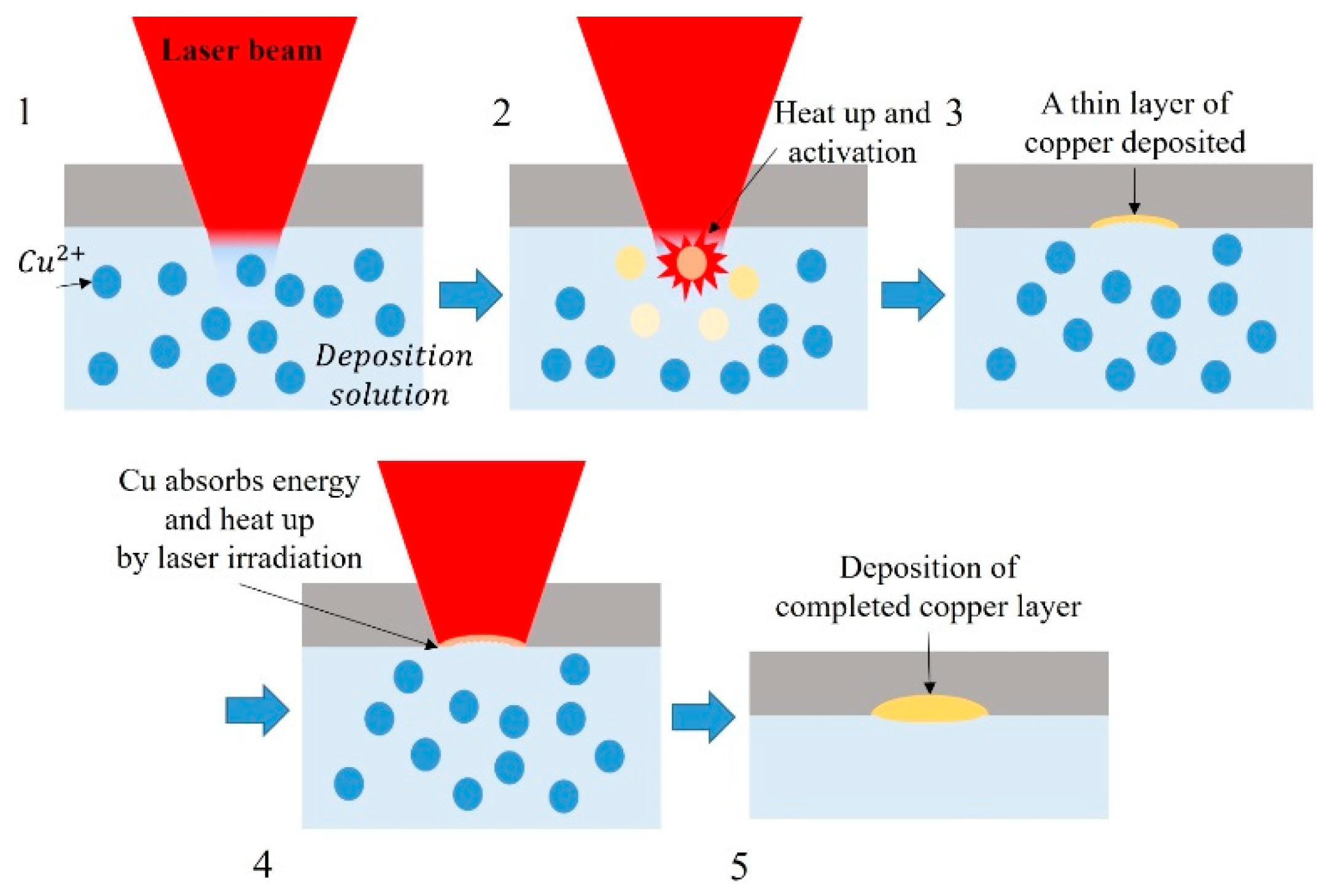
2.1. Laser-Induced Chemical Liquid Phase Deposition

Electroless plating, known as chemical or auto-catalytic plating, is a non-galvanic plating method that involves several simultaneous reactions in a chemical solution, which occur without external electrical power. Unlike electro-plating, it can be applied to various substrates, such as glass or ceramics [19,20]. For obtaining good electroless plating, the selection of deposition solution and process environment is very important.
A commonly used electroless copper deposition method is based on a reduction reaction of copper ions. The main chemical reactions are shown in Equation (1) [21]:
[ Cu ( L ) 2 ] 2 + 2 HCOH + 4 OH + Energy Cu 0 + 2 L 2 + H 2 + H 2 O + 2 HCOO
As can be seen from Equation (1), the electroless deposition reaction consists of four main elements: copper ions, ligand (L), reducing agent (HCOH), and OH-ions. Heat at 60 to 90 degrees Celsius is applied to this solution for several minutes or more to activate the chemical reduction reaction. However, in heating the entire solution in this way, it is impossible to form a selective circuit pattern unless an additional process is added. Therefore, local thermal energy can be applied to an arbitrary pattern by using a laser, thereby enabling the activation of a selective reduction reaction of copper ions within a short time [22].
Figure 1 is a schematic diagram of the LCLD process used in this study. When a near-infrared laser with a wavelength of 1064 nm is irradiated on the upper surface of the glass, it reacts with the deposition solution on the lower surface after passing through the material because of the high transmittance of glass. Accordingly, the temperature of the deposition solution in the selective area irradiated with the laser increases instantaneously, thereby activating the reduction reaction. As a result, a very thin layer of copper begins to form. Additionally, it is possible to obtain a dense copper deposition layer by continuously irradiating a laser to apply thermal energy. At this time, if the energy is excessively high, the process is performed while destroying the thinly deposited copper, so the deposition layer is not formed in the middle part of the laser beam, and the deposition layer remains only in the peripheral part. Therefore, the process was mainly carried out in previous studies with very low energy and feed rates [12,18]. However, even under high laser power conditions, a faster and more stable process will be possible if a condition that can activate the reduction reaction by the laser while diversifying the laser irradiation pattern to minimize direct damage to the copper deposition layer.
Therefore, in this study, an LCLD solution was prepared based on a common electroless plating solution, as shown in Table 1. The possibility of process speed and quality improvement through various laser pattern changes was tested using this approach. CuSO4, which is generally readily available and has excellent reactivity, was used as the main reagent for supplying copper ions. As the ligand, ethylenediaminetetraacetic acid (C10H16N2O8; EDTA) was used, and formaldehyde was chosen as the reducing agent. For a stable chemical reaction, the pH was maintained at 12.6 during the process using NaOH, and a small amount of 2.2 dipyridyl reagent was added.

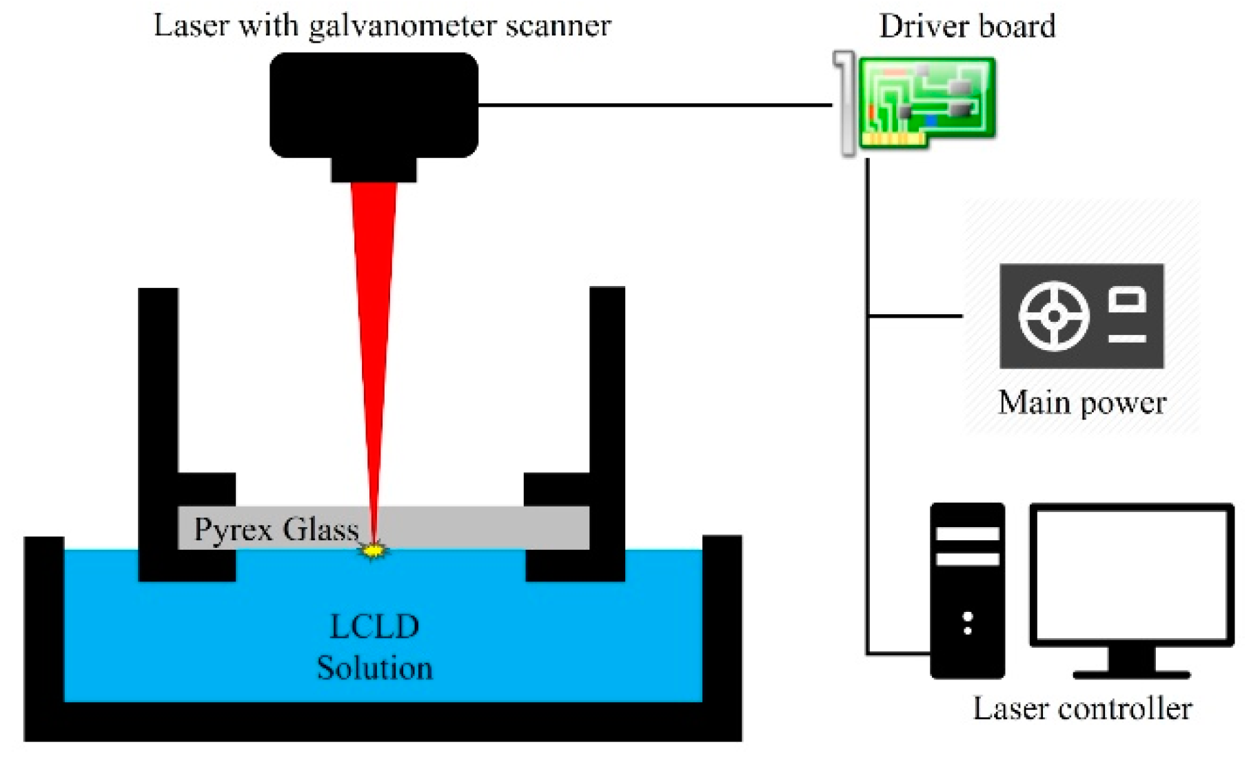
2.2. Experimental Device

A schematic diagram of the LCLD system is shown in Figure 2. A near-infrared (NIR) fiber laser (SP-20P-HS, SPI corporation, Southampton, UK) having a wavelength of 1064 nm was used as the irradiating source. This laser can be operated in either the continuous wave (CW) mode or pulse mode (PM) with a pulse width of 200 ns. The maximum output power was 20 W. A galvanometer scanner (6220H, Cambridge Technology, Bedford, MA, USA) was used to control the scanning path of the laser beam using the EzCad software (EzCad2.1.4, JCZ, Beijing, China). The scanning speed range of the laser beam was 1~1000 mm/s. An F-theta lens with a focal length of 163 mm was used to scan and focus the laser beam. Therefore, the beam spot diameter was approximately 55 µm at the optimized setting. The specifications of the laser system are given in Table 2.
A digital multi-meter (FLUKE 115, FLUKE, Everett, WA, USA) was used to identify the resistance of the specimens. A jig was used to maintain the probe spacing at 10 mm for a stable measure of resistance. A potentiostat/galvanostat (SP-50, BioLogics, Seyssinet-Pariset, France) was used to measure resistance and draw the current-voltage curve accurately. The potentiostat was operated using a scan rate of 0.02 mV/s with a resolution of 5 µV. A surface profile measuring instrument (LT-9010M, Keyence, Osaka, Japan) was used to measure the deposited and the bare surface profile. To observe the microstructure and elemental composition of the specimens, scanning electron microscopy (SEM, VEGA3 LM, TESCAN, Brno-Kohoutovice, Czech Republic) was used.

3. Results and Discussion

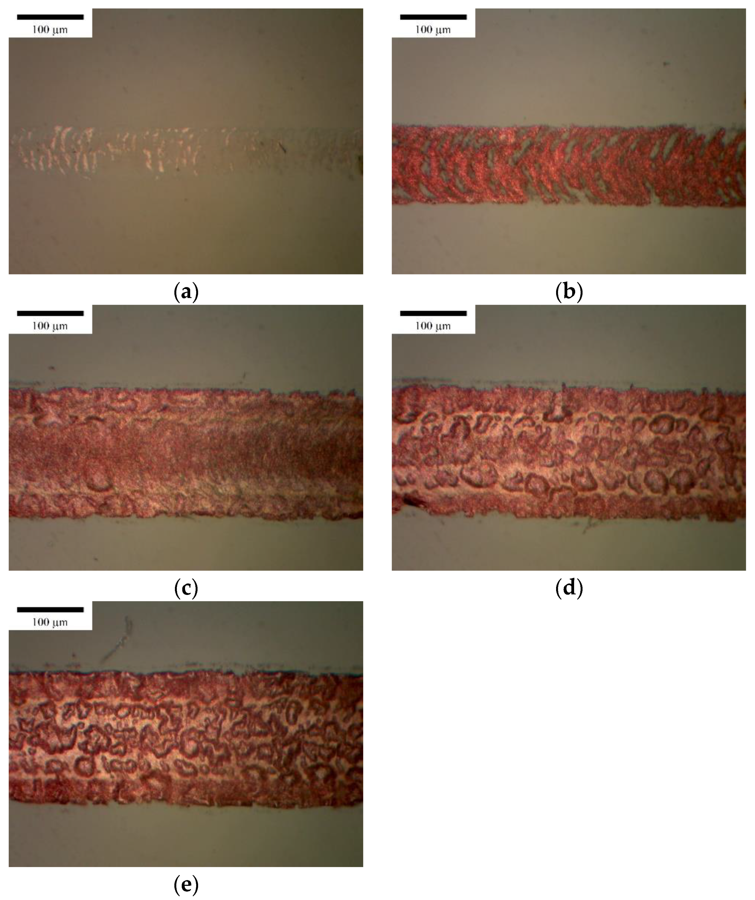
3.1. Horizontal Line
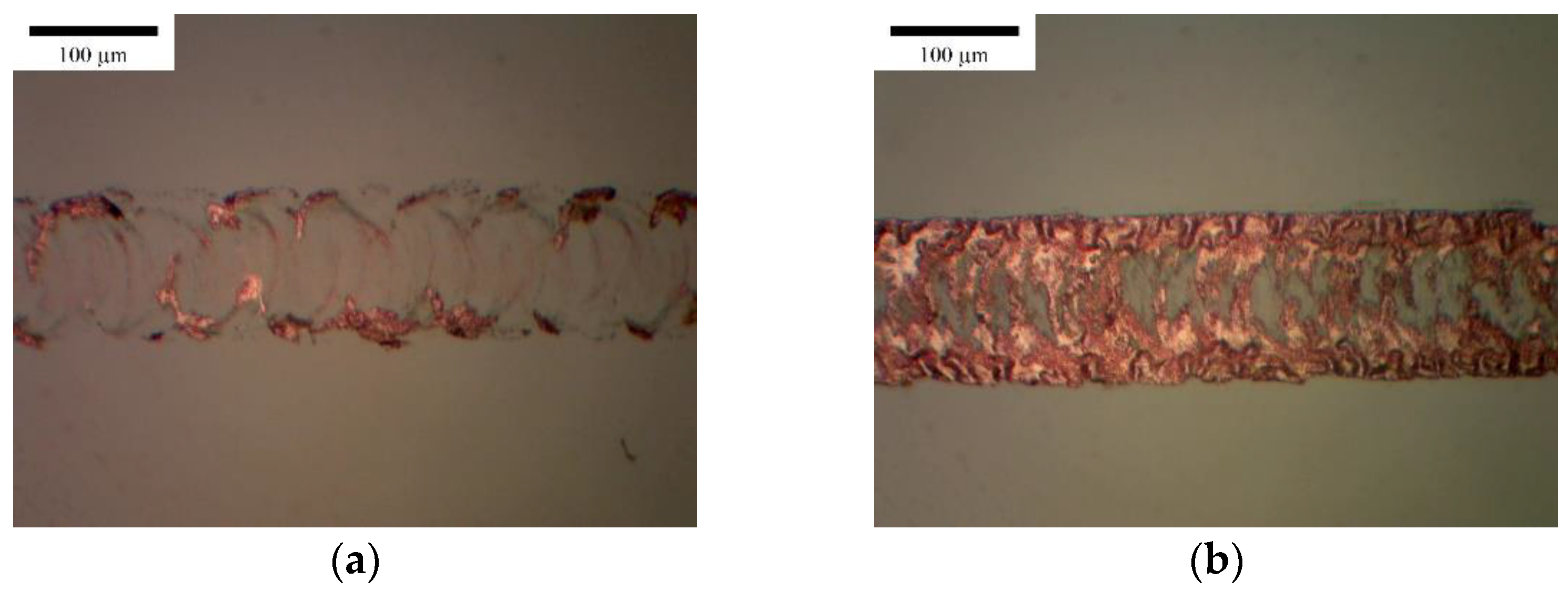
In previous LCLD studies, to minimize direct ablation of deposited copper particles by laser, most of them used low laser power of 0.1~3 W. Accordingly, the feed rate of the laser beam was very low of 0.0025 to 0.015 mm/s to activate the chemical reaction by applying sufficient thermal energy to the reaction area even with low laser power [13,16,18,23]. On the other hand, in this study, to overcome such low productivity, experiments were conducted by increasing the laser power and feed rate more than 10 times. Therefore, the average power was fixed at 20 W, the maximum power generated by the used equipment. The laser scan speed was fixed at 1 mm/s, which is the minimum feed speed of the galvanometer scanner. To maximize the thermal effect, the laser mode was set to continuous wave (CW) mode. In the case of patterning the lines repeatedly, the line interval, which is the center-to-center interval, was fixed at 20 µm so that the overlapping ratio between lines was 50% or more for dense deposition.
Compared with previous studies, the thermal energy for the reduction reaction was relatively insufficient on a single line basis, so only a small amount of copper ions were reduced and deposited, as shown in Figure 3b. Accordingly, the number of lines was increased to 3 and 5 for obtaining a dense and complete conductive line. Through this, the laser energy was repeatedly irradiated to the local area to increase the thermal energy effect, thereby obtaining a more improved deposition result, as shown in Figure 3c,d. However, it could be seen that the deposition was mainly performed on one edge of a laser-irradiated horizontal line. This was due to the following reasons. First, in this experiment, unlike existing LCLD studies, because a high-power laser was irradiated to the deposition solution, bubbles were generated, and these bubbles expanded/exploded and pushed the reduced copper atoms to the edge region. This phenomenon is also commonly observed in the LIBWE process similar to LCLD [12,24,25]. In addition, since high laser power was used in this experiment, the deposited thin copper layer during the first scan was partially ablated at the overlapping area when the next laser scan was irradiated. Thus, in this experiment, when the scan paths of the horizontal line descend in order from top to bottom, the copper was deposited on the edge of the line, but the copper formed on the lower edge of the line was ablated during the next laser scan. As can be seen from the results, the deposition area was mainly observed only at one edge of the line.

3.2. Vertical Line

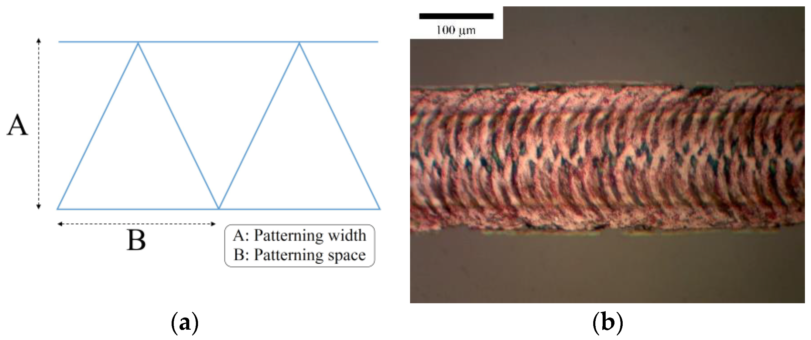
3.2.1. Effect of Patterning Space

In the previous horizontal line test, when the feed rate was increased, even though the average laser power was increased together, time and energy for the chemical reduction reaction were insufficient, indicating that the desired metal deposition was impossible. In addition, when the number of lines was increased to activate the reduction reaction, unintended ablation of the thin copper layer occurred in the overlapping region, making it difficult to obtain a stable conductive structure. Therefore, focusing on the fact that deposition was well performed on one edge where the laser was not directly overlapped according to the direction of the scan path, a vertical line shape scan path was used, as shown in Figure 4a. In this case, if the laser scan proceeded from left to right, the copper deposited on the right edge of the vertical line would continue to ablate, but the copper deposited on the left edge would continue to accumulate and be densely deposited. Accordingly, it was expected that a completed conductive line could be obtained if the vertical line scan was continuously performed. At this time, the length of the patterning width A, which determines the line width of the finally formed conductive line, was fixed to 50 μm, similar to the laser beam diameter. This made it possible to form a conductive line with a width of 100~200 μm similar to the previous studies. The process results were observed while reducing the size of patterning space B, which affected the processing speed and energy density per unit area by every half from 100 μm.
As shown in Figure 4b, when the length of B was 100 µm, traces of deposition by the copper reduction were observed, but sufficient reduction reactions did not occur stably. On the other hand, it could be seen that when the length of B was reduced, the thermal energy by the laser increased. Thus, the formation of the deposited structure by the reduction reaction was significantly improved. When B was 25 µm, the deposited structure with the connected line shape could be obtained, but the conductivity was very unstable. As shown in Figure 4d, there was a section in which unstable deposition occurred due to the excessive gap between the laser pattern and the pattern.
On the other hand, when B was reduced to 12.5 µm or less, a completely connected conductive deposition line structure could be obtained. When B was reduced to 6 µm, a denser deposited structure could be obtained, but it could be seen that the line width was irregularly formed due to excessive energy. Therefore, in this study, patterning space B was selected as 12.5 µm. The deposited line width was 185 µm, and the laser patterning time required to fabricate a 10 mm long conductive line was about 80 s. Compared to previous studies, when converted to the horizontal feed rate of one straight line, it was about 0.124 mm/s. It was found that both the energy used and the process speed increased by about 10 times compared to the previous studies.

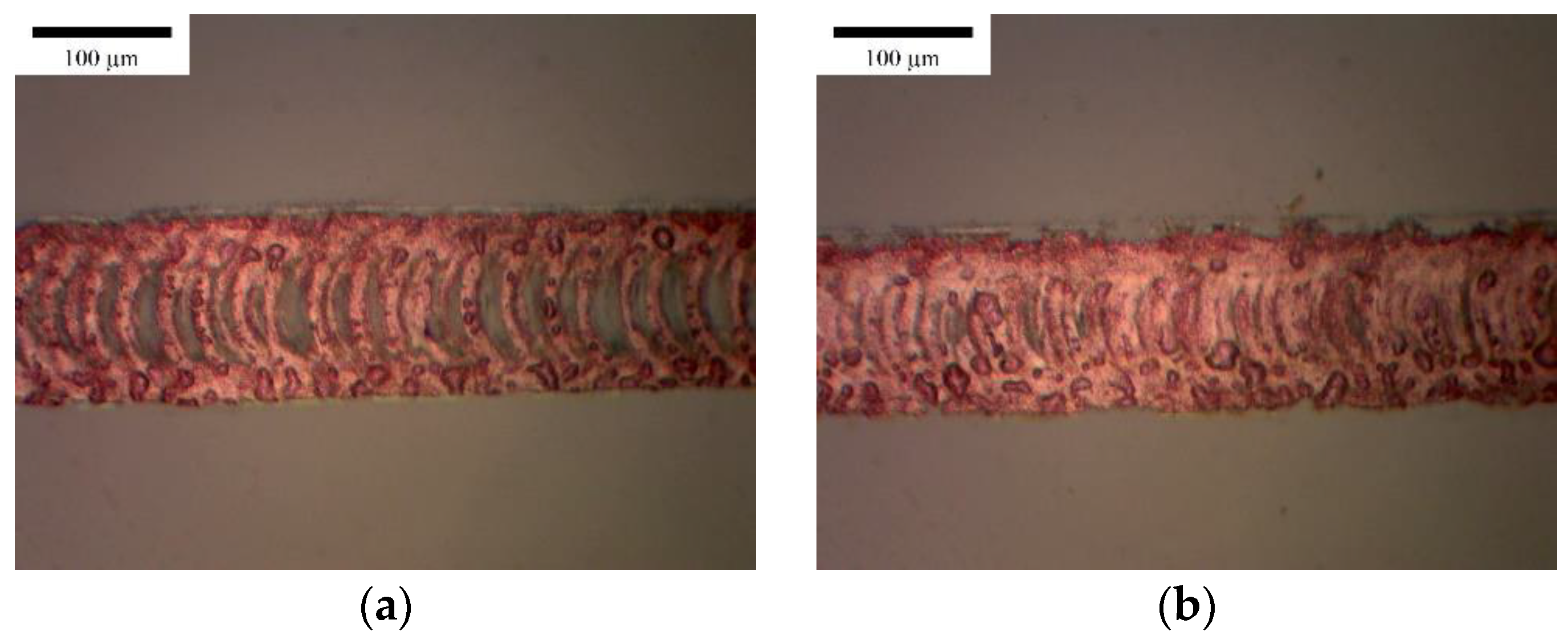
3.2.2. Effect of Frequency

Based on the results obtained from the previous experiment, the effect of the laser frequency on the deposition was examined. The laser pattern used in the experiment was applied in the same shape as in Figure 4a, and A was fixed at 50 µm and B at 12.5 µm. The average laser power was fixed at 20 W, and the scan speed was 1 mm/s, and only the frequency was changed to 25~500 kHz. In addition, the CW mode was also tested.
As shown in Figure 5, the stability of the deposited structure significantly increased as the laser frequency increased. If the laser’s average power is fixed, the laser energy per pulse is changed in inverse proportion to the frequency. Therefore, in the laser ablation process, the energy per pulse is increased by lowering the frequency for vaporizing the material with instantaneous high energy. On the other hand, heating the substrate, such as welding or chemical reaction, the high frequency or CW mode is generally used to maintain a stable temperature rise by continuously applying constant energy. In the LCLD process, it is very important to maintain a uniform temperature rise because chemical reduction is the main reaction. Therefore, in this study, stable deposition was performed when the frequency was over 250 kHz. The following experiments were carried out while fixing the laser mode as the CW, which is widely used in chemical reactions.

3.2.3. Effect of Patterning Width

As seen from the previous experiments, when the patterning width A was 50 µm, a conductive deposited structure with a line width of about 185 µm was obtained. Therefore, the experiment was conducted to obtain a conductive structure with a narrower width by reducing the patterning width A of Figure 4a, which directly affects the deposited line width to 10 µm.
As shown in Figure 6a, when the pattering width was reduced to 10 µm while the patterning space was kept at 12.5 µm, deposition structure was observed in only a few areas. This is because the horizontal feed rate of the line structure increased more than four times compared to the previous experiment as the laser scanning length decreased due to the decrease in the patterning width. That is, the reduction reaction was unstable because of the insufficient heat energy. Therefore, for selective heat energy supply and stable reduction reaction, the experiment was conducted by reducing the patterning space B to 2.5 µm, a fifth of the previous one. When the pattering space B was reduced, since the laser patterning length is increased, the horizontal feed rate of the line structure becomes 0.124 mm/s, the same value as when a stable deposition structure was formed in the previous experiment. However, even though the horizontal feed rate was kept at a low level by reducing the pattering space B in this way, a deposition structure was connected to each other only at the edge region, as shown in Figure 6b. The middle region of the line was deposited in a discontinuous structure. This was because the high-powered laser beam was excessively overlapped due to the reduced pattering space. The deposited copper thin layer was ablated in the middle region where the energy density was high, thereby preventing the formation of the stable deposited structure.

3.3. Various Scan Path

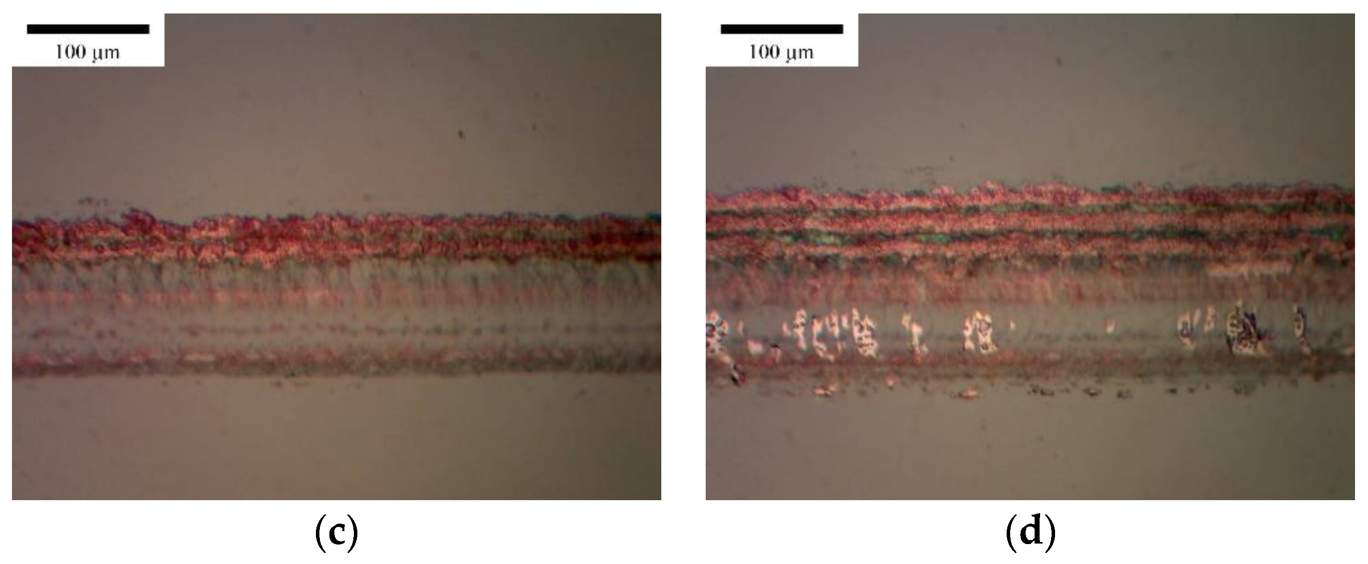
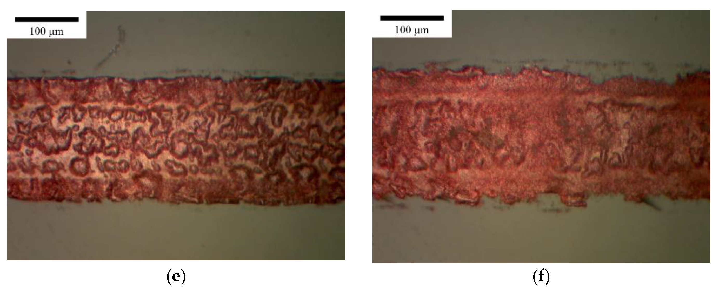
3.3.1. Deposition according to Scan Path

In the LCLD process, the horizontal feed rate of the line structure must be lowered to a certain level for sufficient selective heat energy supply and a stable reduction reaction. Therefore, to obtain a narrow line width, the patterning width and the patterning space should be reduced to maintain the horizontal feed rate. For this reason, when irradiating the laser through the vertical line shape scan path, ablation occurred due to high energy overlap in the middle region, making it impossible to form a stable deposited structure. Accordingly, the experiment was conducted by changing the scan path design to reduce the excessive overlap of the laser beam while lowering the horizontal feed rate below a certain level.
From the previous chapters, it can be seen that deposition was effectively performed mainly at the edge of the laser scan path, and ablation occurred in the middle region where the energy density was highest, which had a negative effect on the deposition. Therefore, as shown in Figure 7a, a new triangular scan path was designed by adding a scan path to the outer region of the vertical line. In this case, since the entire laser patterning proceeded while surrounding the deposited structure, the laser beam was expected to produce a stable deposited structure through indirect heating. Patterning width A and patterning space B were fixed at 50 µm and 20 µm, respectively, so that the horizontal feed rate was 0.141 mm/s. However, as shown in Figure 7b, some unstable deposition was observed in the middle region, although the deposition structure was formed. Accordingly, laser patterning was designed in a form surrounding the deposited structure. Still, the scan path was modified in an elliptical shape, as shown in Figure 8a, to minimize ablation due to excessive energy overlap in a small area.
In order to deposit a similar line width structure of the previous experiments, the major axis length A of the ellipse was set to 50 µm. In order to irradiate energy evenly over the entire pattern area, the distance between the ellipse centers was fixed at half of the length B. At this time, the major axis length B of the ellipse was set to 50 µm, so that the horizontal feed rate was 0.159 mm/s, a similar level to that of the previous experiment. As shown in Figure 8b, a conductive structure with a line width of about 180 µm, completely connected as a single line, was obtained.

3.3.2. Reduction of Line Width

In order to reduce the line width at the elliptical scan path, which was advantageous for the dispersion of laser energy, the minor axis length A was reduced to 5 µm. When the major axis length B was set to 50 µm, as shown in Figure 9a, a conductive structure with a significant incomplete deposition area in the middle of the line was formed. Accordingly, as a result of the experiment by reducing the major axis length B to 25 µm, a significant part of the incomplete deposition area was improved, as shown in Figure 9b, and a conductive structure with a line width of 130 µm was obtained. This was because the elliptical scan path was more advantageous in dispersing the laser energy than the scan path based on the previous vertical line. Even when the line width was reduced, as in this experiment, it was possible to suppress unnecessary ablation by minimizing laser beam overlapping.

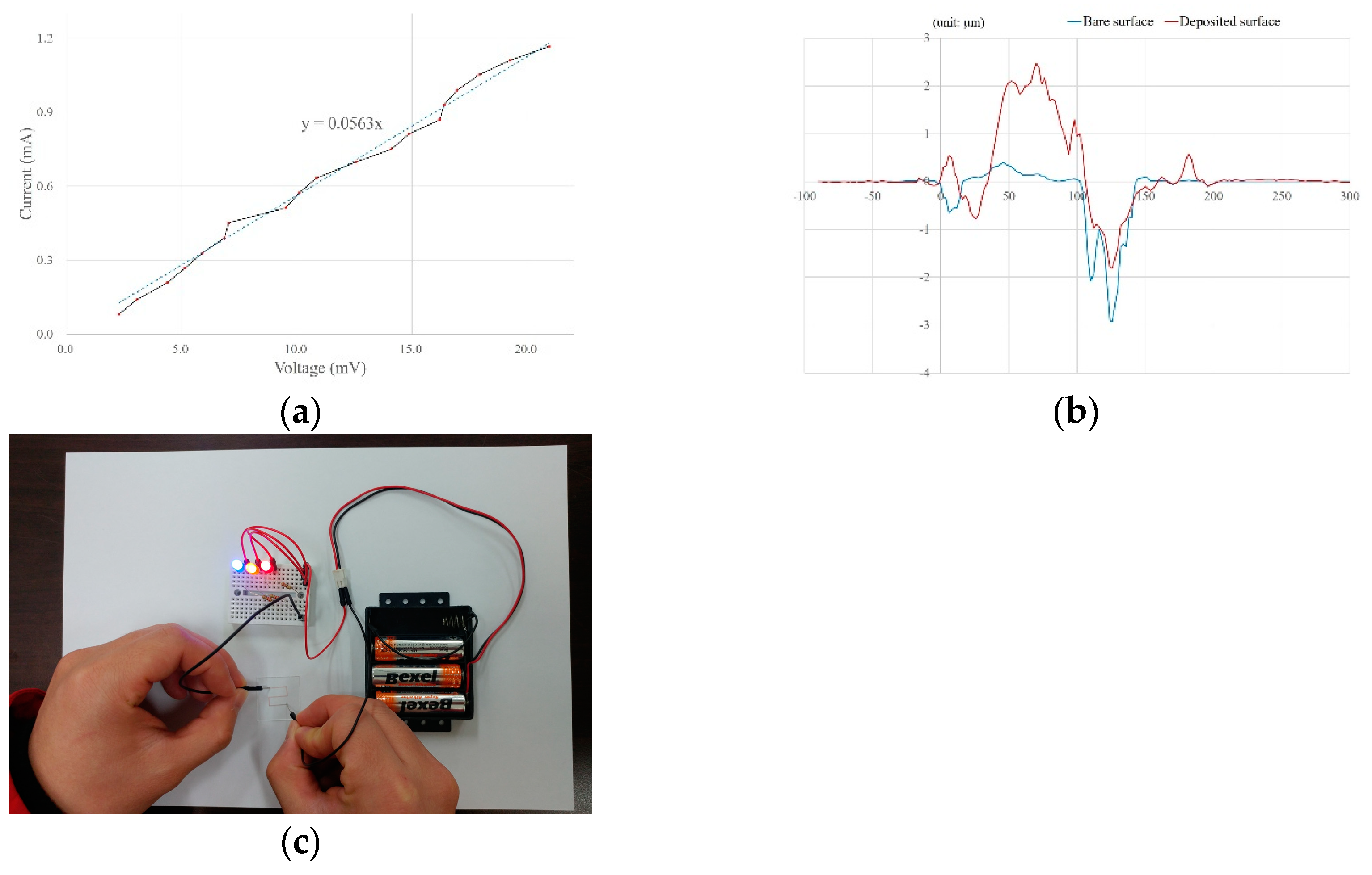
3.3.3. Specific Resistance and Applications

The previous experiments fabricated a conductive structure using the elliptical scan path in which the most stable deposition was performed, and the specific resistance was measured. The length of the major and minor axes was set equally to 50 µm, and the laser mode was set to CW. For calculating the specific resistance of the fabricated conductive structure, current-voltage curve was measured using potentiostat/galvanostat. The length of the measured conductive structure was 1.0 × 10⁻² m, and the resistance of the conductive structure was calculated as 17.762 Ω from Figure 10a. Based on this value, the specific resistance was found to be 26.1 μΩ·cm. As shown in Table 3, compared to bulk copper or common electroless plating, the specific resistance was more than 10 times higher. Still, compared to previous LCLD studies, it showed relatively superior performance [26]. In addition, the specific resistance in the LCLD is closely related to the process speed [27]. Therefore, the proposed process was more than 10 times faster than the previous LCLD process and at the same time had a low level of specific resistance, so it could be considered that the economic feasibility and quality had improved significantly.

4. Conclusions

LCLD is a well-known selective deposition process because of its simplicity and cost-effectiveness. It can also fabricate quite small-sized conductive lines based on relatively inexpensive laser equipment. Despite the many advantages of the LCLD process, since it is based on a chemical reduction reaction by local heating, it has a fatal disadvantage: the process speed is very slow. Therefore, in this study, experiments were conducted to improve the process speed through various conditions change based on relatively high laser power.
When the process speed was increased based on the horizontal line shape scan path, which was mainly used in previous studies, deposition was hardly performed due to insufficient time and thermal energy for a stable reduction reaction. When repeating the laser scan loop, it could be seen that the deposition structure was formed around the edge of the scan path. Utilizing this phenomenon, if laser scan proceeded in one direction with partially overlapped, the reduction reaction could be activated due to the increase in the thermal energy of the overlapping regions, enabling the formation of a dense deposited structure at the edge of the scan path. From this, as a result of conducting an experiment based on a scan path having a vertical line, triangular, and elliptical shape, the most stable deposition result was obtained at the elliptical scan path. The elliptical scan path was more advantageous in dispersing laser energy than the general line-based scan path. Thus, the activation region of the reduction reaction by selective heat up could be widened. This made it possible to secure the time required for the stable chemical reduction and reduce unwanted ablation phenomenon by excessive overlap. Therefore, the proposed fast LCLD process was able to fabricate a conductive line with a specific resistance of 26.1 µΩ·cm, while improving the process speed by 10 times more compared to the previous LCLD studies. It was also confirmed that the fabricated pattern could play the role of a circuit. That is, the proposed fast LCLD process was an inexpensive and low-temperature process that could quickly form a conductive pattern with a single process, and it was possible to realize excellent conductivity while minimizing the influence on other pre-mounted parts.

Author Contributions

Conceptualization, M.-S.P.; methodology, M.-S.P.; investigation, H.-G.K. and M.-S.P.; writing—original draft preparation, H.-G.K. and M.-S.P.; writing—review and editing, M.-S.P.; supervision, M.-S.P.; project administration, M.-S.P.; funding acquisition, M.-S.P. All authors have read and agreed to the published version of the manuscript.

Funding

This study was supported by the Research Program funded by SeoulTech (Seoul National University of Science and Technology).

Institutional Review Board Statement

Not applicable.

Informed Consent Statement

Not applicable.

Data Availability Statement

Not applicable.

Conflicts of Interest

The authors declare no conflict of interest. The funders had no role in the design of the study; in the collection, analyses, or interpretation of data; in the writing of the manuscript, or in the decision to publish the results.

References

  1. Crawford, G.P. Flexible Flat Panel Displays; John Wiley & Sons, Ltd.: Chichester, UK, 2005; ISBN 9780470870501. [Google Scholar]
  2. Han, M.J.; Khang, D.-Y. Glass and Plastics Platforms for Foldable Electronics and Displays. Adv. Mater. 2015, 27, 4969–4974. [Google Scholar] [CrossRef]
  3. Nam, K.G.; Cho, S.H.; Chang, W.S.; Na, S.J.; Whang, K.H.; Kim, J.G. Micromachining Characteristics inside Transparent Materials using Femtoseocond Laser Pulses. J. Korean Soc. Precis. Eng. 2006, 23, 190–196. [Google Scholar]
  4. Chen, M.F.; Chen, Y.P.; Hsiao, W.T.; Gu, Z.P. Laser direct write patterning technique of indium tin oxide film. Thin Solid Films 2007, 515, 8515–8518. [Google Scholar] [CrossRef]
  5. Wang, M.W.; Liu, T.Y.; Pang, D.C.; Hung, J.C.; Tseng, C.C. Inkjet printing of a pH sensitive palladium catalyst patterns of ITO glass for electroless copper. Surf. Coat. Technol. 2014, 259, 340–345. [Google Scholar] [CrossRef]
  6. Hon, K.K.B.; Li, L.; Hutchings, I.M. Direct writing technology-Advances and developments. CIRP Ann.-Manuf. Technol. 2008, 57, 601–620. [Google Scholar] [CrossRef]
  7. Choi, S.; Park, M. Fabrication of Conductive Patterns on 3D Printed Structure Using Photo-Polymerization Technology. Phys. Status Solidi 2019, 216, 1801017. [Google Scholar] [CrossRef]
  8. Shin, I.J.; Park, M.S. Direct Conductive Patterning on 3D Printed Structure Using Laser. Phys. Status Solidi 2018, 215, 1700597. [Google Scholar] [CrossRef]
  9. Shin, I.; Park, M. 3D printed conductive patterns based on laser irradiation. Phys. Status Solidi 2017, 214, 1600943. [Google Scholar] [CrossRef]
  10. Hanada, Y.; Sugioka, K.; Midorikawa, K. Selective metallization of photostructurable glass by femtosecond laser direct writing for biochip application. Appl. Phys. A Mater. Sci. Process. 2008, 90, 603–607. [Google Scholar] [CrossRef]
  11. Sugioka, K.; Masuda, M.; Hongo, T.; Cheng, Y.; Shihoyama, K.; Midorikawa, K. Three-dimensional microfluidic structure embedded in photostructurable glass by femtosecond laser for lab-on-chip applications. In Proceedings of the Applied Physics A: Materials Science and Processing; Springer: Berlin/Heidelberg, Germany, 2004; Volume 79, pp. 815–817. [Google Scholar]
  12. Kim, H.-G.; Park, M.S. Circuit patterning using laser on transparent material. Surf. Coatings Technol. 2017, 315, 377–384. [Google Scholar] [CrossRef]
  13. Kochemirovsky, V.A.; Fateev, S.A.; Logunov, L.S.; Tumkin, I.I.; Safonov, S.V. Laser-induced copper deposition with weak reducing agents. Int. J. Electrochem. Sci. 2014, 9, 644–658. [Google Scholar] [CrossRef] [Green Version]
  14. Kochemirovsky, V.A.; Khairullina, E.M.; Safonov, S.V.; Logunov, L.S.; Tumkin, I.I.; Menchikov, L.G. The influence of non-ionic surfactants on laser-induced copper deposition. Appl. Surf. Sci. 2013, 280, 494–499. [Google Scholar] [CrossRef]
  15. Manshina, A.A.; Povolotskiy, A.V.; Ivanova, T.Y.; Tver’Yanovich, Y.S.; Tunik, S.P.; Kim, D.; Kim, M.; Kwon, S.C. Effect of salt precursor on laser-assisted copper deposition. Appl. Phys. A Mater. Sci. Process. 2007, 89, 755–759. [Google Scholar] [CrossRef]
  16. Tumkin, I.I.; Kochemirovsky, V.A.; Bal’makov, M.D.; Safonov, S.V.; Zhigley, E.S.; Logunov, L.S.; Shishkova, E.V. Laser-induced deposition of nanostructured copper microwires on surfaces of composite materials. Surf. Coat. Technol. 2015, 264, 187–192. [Google Scholar] [CrossRef]
  17. Kochemirovsky, V.A.; Skripkin, M.Y.; Tveryanovich, Y.S.; Mereshchenko, A.S.; Gorbunov, A.O.; Panov, M.S.; Tumkin, I.I.; Safonov, S. V Laser-induced copper deposition from aqueous and aqueous–organic solutions: State of the art and prospects of research. Russ. Chem. Rev. 2015, 84, 1059–1075. [Google Scholar] [CrossRef]
  18. Seo, J.M.; Kwon, K.-K.; Song, K.Y.; Chu, C.N.; Ahn, S.-H. Deposition of Durable Micro Copper Patterns into Glass by Combining Laser-Induced Backside Wet Etching and Laser-Induced Chemical Liquid Phase Deposition Methods. Materials 2020, 13, 2977. [Google Scholar] [CrossRef]
  19. Chong, E.K.; Stevens, M.G.; Nissen, K.E. Effect of surface roughness on the adhesion of electrolessly plated platinum to poly(ethylene terephthalate) films. J. Adhes. 2003, 79, 667–681. [Google Scholar] [CrossRef]
  20. Bugaev, S.P.; Sochugov, N.S. Production of large-area coatings on glasses and plastics. In Proceedings of the Surface and Coatings Technology; Elsevier: Amsterdam, The Netherlands, 2000; Volume 131, pp. 474–480. [Google Scholar]
  21. Kochemirovsky, V.A.; Menchikov, L.G.; Kuz’Min, A.G.; Safonov, S.V.; Tumkin, I.I.; Tver’Yanovich, Y.S. Side reactions during laser-induced deposition of copper from aqueous solutions of CuII complexes. Russ. Chem. Bull. 2012, 61, 1041–1047. [Google Scholar] [CrossRef]
  22. Wang, X.C.; Zheng, H.Y.; Lim, G.C. Laser induced copper electroless plating on polyimide with Q-switch Nd:YAG laser. Appl. Surf. Sci. 2002, 200, 165–171. [Google Scholar] [CrossRef]
  23. Kochemirovsky, V.A.; Khairullina, E.M.; Safonov, S.V.; Logunov, L.S.; Tumkin, I.I.; Menchikov, L.G. Influence of surfactants on laser-induced copper deposition from solution. Russ. Chem. Bull. 2014, 62, 1570–1578. [Google Scholar] [CrossRef]
  24. Huang, Z.Q.; Hong, M.H.; Do, T.B.M.; Lin, Q.Y. Laser etching of glass substrates by 1064 nm laser irradiation. Appl. Phys. A 2008, 93, 159–163. [Google Scholar] [CrossRef]
  25. Xie, X.; Huang, X.; Jiang, W.; Wei, X.; Hu, W.; Ren, Q. Three dimensional material removal model of laser-induced backside wet etching of sapphire substrate with CuSO4 solutions. Opt. Laser Technol. 2017, 89, 59–68. [Google Scholar] [CrossRef]
  26. Zehnder, S.; Schwaller, P.; Arx, U.V.; Neuenschwander, B. Laser-Induced Chemical Liquid-Phase Deposition of Copper on Transparent Substrates. In Proceedings of the International Conference on Advanced Laser Technologies, Thun, Switzerland, 2–6 September 2012. [Google Scholar]
  27. Chen, Q.J.; Imen, K.; Allen, S.D. Laser Enhanced Electroless Plating of Micron-Scale Copper Wires. J. Electrochem. Soc. 2000, 147, 1418. [Google Scholar] [CrossRef]
  28. Li, J.; Shi, T.; Feng, C.; Liang, Q.; Yu, X.; Fan, J.; Cheng, S.; Liao, G.; Tang, Z. The novel Cu nanoaggregates formed by 5 nm Cu nanoparticles with high sintering performance at low temperature. Mater. Lett. 2018, 216, 20–23. [Google Scholar] [CrossRef]
Figure 1. Principles of the LCLD process: (1) Laser irradiates from the top; (2) The copper ion reduction reaction occurs after heating up solution; (3) A thin layer of copper is deposited on the bottom of the glass; (4) The solution and the deposited Cu absorbs the laser energy and heats up the near area; (5) Dense copper layer is deposited on the bottom of the glass.
Applsci 11 08695 g001
Figure 2. Schematic diagram of LCLD system.
Applsci 11 08695 g002
Figure 3. Horizontal scan result according to number of lines: (a) schematic diagram; (b) single line; (c) 3 lines; (d) 5 lines.
Applsci 11 08695 g003aApplsci 11 08695 g003b
Figure 4. Vertical scan result according to patterning space B: (a) schematic diagram; (b) 100 µm; (c) 50 µm; (d) 25 µm; (e) 12.5 µm; (f) 6 µm.
Applsci 11 08695 g004aApplsci 11 08695 g004b
Figure 5. Vertical scan result according to laser frequency: (a) 25 kHz; (b) 100 kHz; (c) 250 kHz; (d) 500 kHz; (e) CW mode.
Applsci 11 08695 g005
Figure 6. Result of reduced patterning width according to patterning space B: (a) 12.5 µm; (b) 2.5 µm.
Applsci 11 08695 g006
Figure 7. Deposition with triangular scan path: (a) schematic diagram; (b) experimental result.
Applsci 11 08695 g007
Figure 8. Deposition with elliptical scan path: (a) schematic diagram; (b) experimental result.
Applsci 11 08695 g008
Figure 9. Result of reducing the minor axis length according to major axis length B: (a) 50 µm; (b) 25 µm.
Applsci 11 08695 g009
Figure 10. Conductivity test of deposited structure: (a) current-voltage curve; (b) profile graph of the deposited and the bare surface; (c) simple application to LED circuit.
Applsci 11 08695 g010
Table 1. Composition of LCLD solution.
ReagentsContents
CuSO415 g/L
EDTA35 g/L
HCHO10 g/L
NaOHpH 12.6
2.2 dipyridyl10 mg/L
Table 2. Main specifications of the Nd:YAG fiber laser.
CharacteristicsTypicalUnit
Working materialNd:YAG
Mode of operationPulsed/Continuous wave
Wavelength1064nm
Maximum output power20W
Pulse width200ns
Pulse repetition rate1–500kHz
Beam quality, M22
Focused beam diameter55μm
Table 3. The specific resistance of the fabricated pattern.
Bulk CopperCommon
Electroless Plating
Cu Nanoparticles
after Sintering [28]
Previous
LCLD Process
Proposed Fast
LCLD Process
Specific resistance [μΩ·cm]1.682.004.3710~30026.1
Publisher’s Note: MDPI stays neutral with regard to jurisdictional claims in published maps and institutional affiliations.

