Article

Beam Profile Characterisation of an Optoelectronic Silicon Lens-Integrated PIN-PD Emitter between 100 GHz and 1 THz

1
ATI, University of Surrey, Guildford GU2 7XH, UK
2
National Physical Laboratory, Teddington TW11 0LW, UK
3
Fraunhofer Institute for Telecommunication, Heinrich Hertz Institute, Einsteinufer 37, 10587 Berlin, Germany
4
Institute of Solid State Physics, Technical University Berlin, Hardenbergstr. 36, 10623 Berlin, Germany
*
Author to whom correspondence should be addressed.
Appl. Sci. 2021, 11(2), 465; https://doi.org/10.3390/app11020465
Submission received: 24 December 2020 / Revised: 29 December 2020 / Accepted: 30 December 2020 / Published: 6 January 2021
(This article belongs to the Special Issue Terahertz Communications)

Abstract

:

Featured Application

This paper can be an important starting point for establishing beam profile measurements as an essential characterization tool for terahertz emitters.

Abstract

Knowledge of the beam profiles of terahertz emitters is required for the design of terahertz instruments and applications, and in particular for designing terahertz communications links. We report measurements of beam profiles of an optoelectronic silicon lens-integrated PIN-PD emitter at frequencies between 100 GHz and 1 THz and observe significant deviations from a Gaussian beam profile. The beam profiles were found to differ between the H-plane and the E-plane, and to vary strongly with the emitted frequency. Skewed profiles and irregular side-lobes were observed. Metrological aspects of beam profile measurements are discussed and addressed.

1. Introduction

In recent years, continuous-wave (CW) Terahertz (THz) radiation has become a promising candidate for short range communication links bridging between fibre-optical networks and wireless transmission, the so-called “THz bridge”. Besides this latest field of applications, THz technology is employed in a wide range of applications such as: spectroscopy [1], bio-medical imaging [2,3], reflection imaging [4], security [5,6], non-destructive testing [7], non-contact imaging for art and archaeological conservation [8,9], and wireless communication links [10,11]. CW THz spectroscopy with photomixing emitters and receivers enables compact sensor heads that cover a broad frequency range of more than 3 THz combined with high sensitivity [1,12,13,14,15,16,17]. In particular, photomixers based on indium phosphide (InP) make it possible to build CW THz systems using off-the-shelf components originally developed for fibre-based telecommunications [13,18,19]. The mature telecom technology enables the development of compact and robust THz systems and even photonic integrated circuits [14,20]. Wireless communication benefits from fibre-coupled THz transceivers since they can be integrated seamlessly into optical communication networks, because they use the same infrastructure, e.g., amplifiers or modulators [10,21,22].
High-speed photodiodes (PD), originally developed as photodetectors for optical communications [23,24], serve as an optoelectronic converter in THz emitters [25,26,27,28,29,30,31]. To produce an optical signal modulated at the desired THz frequency fTHz, two single-mode laser signals (f1, f2) are superposed. The envelope frequency of the resulting beat note is the difference frequency of the laser signals. As long as the PD is capable of following that envelope frequency, a photocurrent is generated equal to fTHZ = |f1f2|. For efficient radiation into free space, a broadband antenna is attached to the diode and the diode is mounted onto a substrate lens [32]. In this work, a waveguide-integrated PIN photodiode with attached bow-tie antenna is employed, which is mounted on a hyper-hemispheric silicon lens and packaged into a fibre-pigtailed housing. A detailed description of this emitter and its THz performance can be found elsewhere [33].
While many aspects of PD devices and THz systems as a whole have been intensively studied, the emitter radiation pattern in the THz domain is generally assumed to be Gaussian. Since mirrors or lenses are commonly employed in spectroscopic and sensing applications, the beam profile of THz emitters remains widely unknown. However, in THz communication links, no beam forming elements can be placed in the free space between the emitter and the receiver. For all applications, but particularly for those involving medium and long-range free-space propagation such as communications, it is important to have a good understanding of the spatial profile of the THz beam. Therefore, an investigation of the beam profile is urgently required to develop transmitters, i.e., antenna structures, dedicated to THz communication links. In microwave and millimetre wave communication systems, the characterization of emitter (transmitter) beam profiles has long since been accepted as an essential tool. In this field, the techniques for antenna characterisation are extensively developed and well understood [34]. Furthermore, specialized facilities are available to perform the required measurements. None of these as yet exist for THz devices. THz radiation is often assumed to propagate as a perfect Gaussian beam, which the present study shows to be inaccurate.
There is very little published literature on measurements of beam profiles of CW THz emitters, with the vast majority of beam profile data describing pulsed systems [35,36,37,38]. This is primarily due to the widespread use of pulsed THz systems for spectroscopy, where beam profile properties may give rise to errors in spectroscopic data. Moreover, pulsed THz emitters have peak powers that are 3–4 orders of magnitude higher than CW devices, facilitating beam characterisation. Of the existing literature on CW beam profiles, most are for high power laser sources with a narrow tuning range such as quantum cascade lasers (QCLs) [39,40] and gas lasers [41].
In this study we performed detailed measurements of the beam profile of a commercial THz emitter based on a PIN photodiode at frequencies between 100 GHz and 1 THz, and for both E-plane and H-plane.

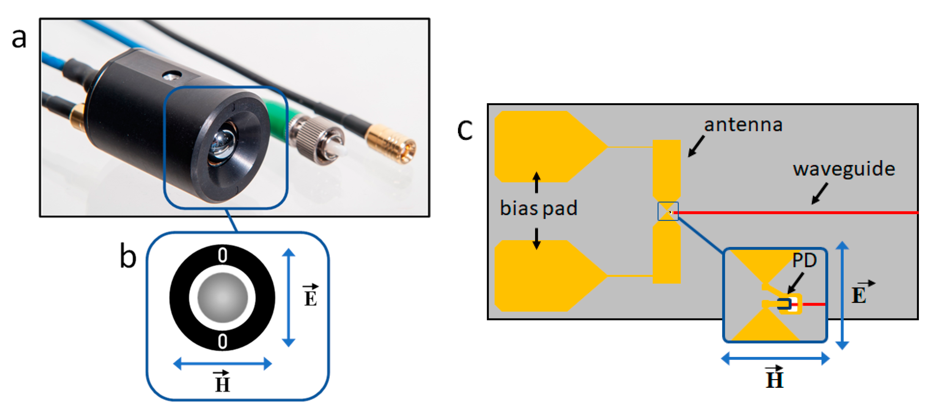
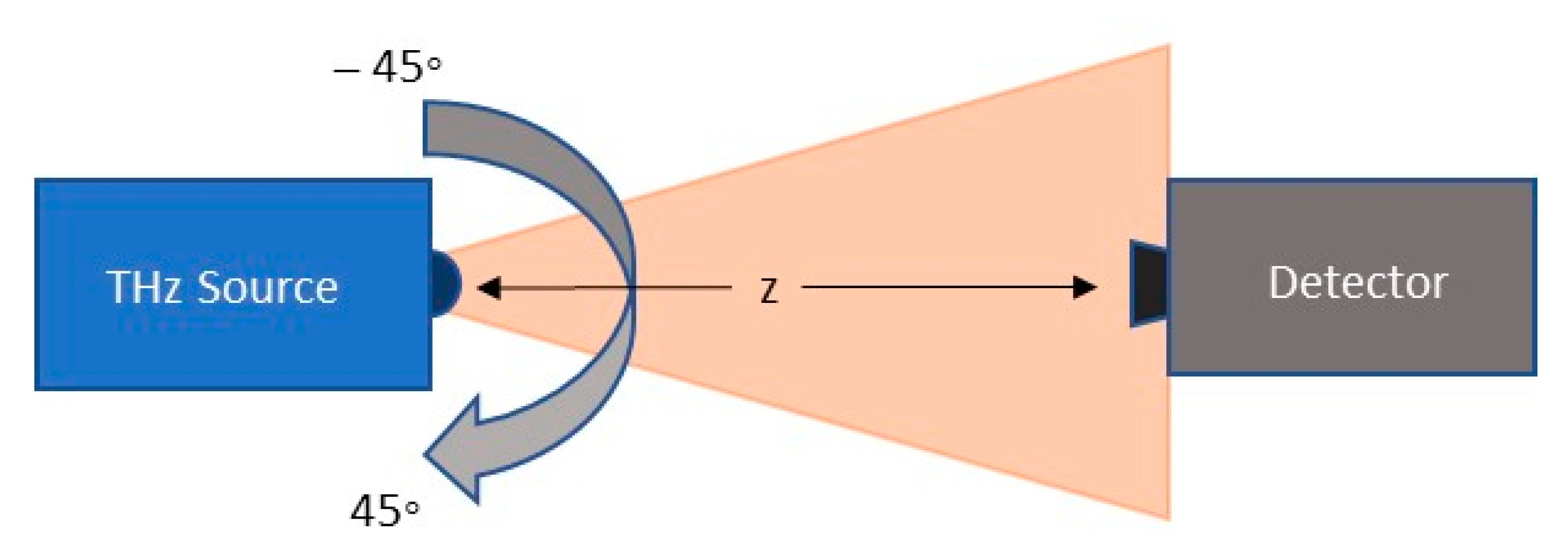
2. Materials and Methods

The PIN diode emitter was fabricated at Fraunhofer HHI in Germany [33]. A diagram of the emitter antenna is shown in Figure 1 with the E- and H- planes indicated. The emitter is mounted onto a hyper-hemispherical high-resistivity silicon (Si) lens with a diameter of 10 mm to reduce both beam divergence [32] and coupling losses (due to Fresnel reflections) from the InP substrate to air. The beam profiles were obtained using an angular mapping method, applied in two orthogonal orientations to yield beam profiles in the E-plane and H-plane. The frequency of the emitter was tuned from 100 GHz to 1 THz.
The beam profile of an emitter can be described by adopting two different approaches: (i) lateral displacement or (ii) angular displacement of the emitter with respect to the receiver. For a collimated beam where lateral dimensions and profile are preserved with distance from the source, lateral mapping is appropriate to describe the beam profile. For a divergent source, angular mapping is more appropriate, because angular spread and variation is preserved with distance from the source. Since the PIN diode emitter examined here is a divergent source, its beam profiles were measured using an angular mapping method.
The angular profiles of both orientations of the emitter were measured using the setup shown in Figure 2. The emitter was placed on a rotary stage and rotated with respect to the detector from −45° to +45° in 0.2° steps. The detector was a Tydex GC-1T Golay cell with an 11-mm aperture. The emitter was powered and controlled by a Toptica TeraScan system. The bias modulation frequency was set to 11.242 Hz, since this was the optimum modulation frequency to maximise the responsivity of the Golay detector. The output of the detector was read by a lock-in amplifier (Signal Recovery 7265 DSP).

3. Results

3.1. Power Measurements

The power output of the emitter, shown in Figure 3a, was measured for frequencies between 50 GHz and 1000 GHz using both a pyroelectric detector (Sensor- und Lasertechnik THZ 10) and a Golay cell (Tydex GC-1T). THz radiation from the emitter was collected and re-focused by two parabolic mirrors, as shown in Figure 3b. The pyroelectric detector was calibrated by the national institute for metrology of Germany (PTB) and was used to measure the emitter power at frequencies between 50 GHz and 500 GHz. Frequencies between 200 GHz and 1000 GHz were measured using the more sensitive Golay cell, and the overlapping measurements between 200 GHz and 500 GHz were used to calibrate the Golay cell responsivity. Measurements were taken in 10 GHz steps.

3.2. Beam Profiles

Angular beam profile measurements for both orientations of the PIN diode emitter were performed with the Golay cell for a frequency range of 100 GHz to 1000 GHz at 50 GHz intervals. The resulting profiles are shown in Figure 4a,b. All profiles were normalised to allow for ease of comparison, since the power ratio between the low and high frequencies is over two orders of magnitude (see Figure 3).
The H-plane profiles in Figure 4a, while not perfectly Gaussian, show a single peak centred around 0° for frequencies below 400 GHz. Between 400 GHz and 600 GHz, the single peak becomes significantly broader and shows significant small features throughout the profile. Above 600 GHz, the centre of the peak skews to the negative angles.
In Figure 4b, the E-plane profiles for frequencies below 250 GHz also show a peak centred at 0°; however, unlike the H-plane profiles, there are also significant side lobes either side of the centre. Above 300 GHz, these side lobes disappear, but the main peak becomes heavily skewed to the positive angles and highly asymmetrical.
While the bow-tie antenna itself is symmetric, the feeding lines and the InP substrate are not. When the wavelength is of a similar order as the dimensions of the feeding point structures or the substrate, those structures start to radiate or cause refraction. The influence of the feeding point geometry on the beam profile is studied in a separate publication.

3.3. Experimental Considerations

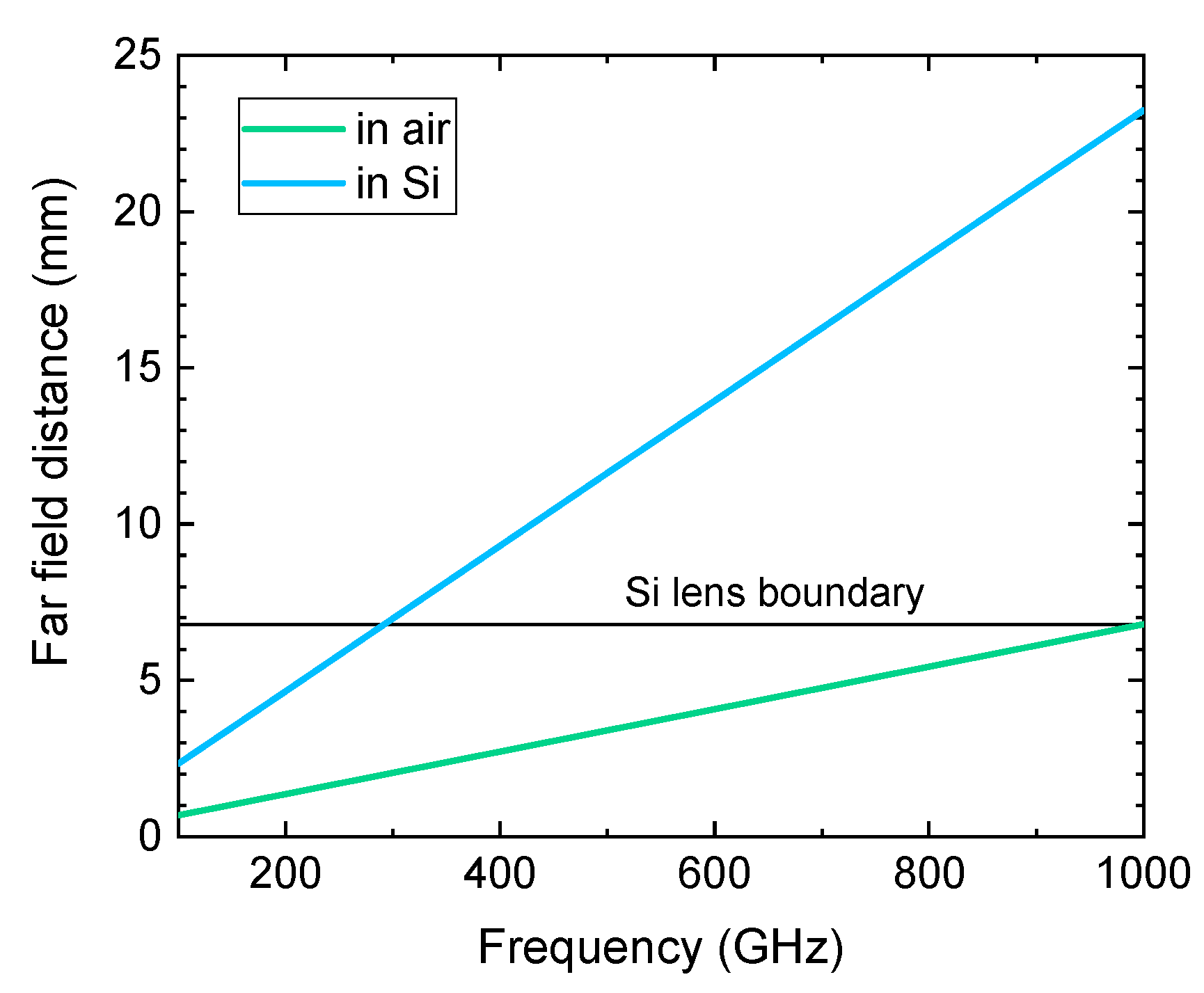
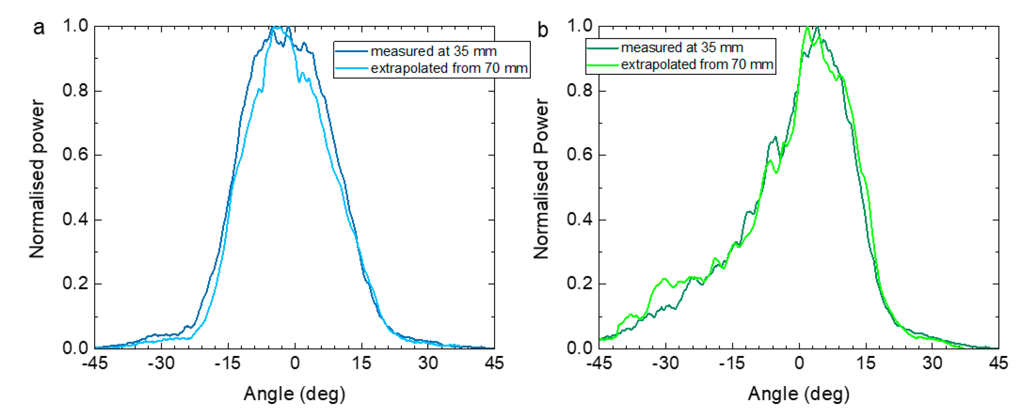
3.3.1. Near Field vs. Far Field

The electromagnetic field of an antenna is commonly described as evolving from the near field region, where the angular distribution of the field varies with distance from the antenna, to the far field region, where the angular distribution is distance-independent. The near-field region may be further divided into the reactive and radiative regions. The reactive near field region decays rapidly with distance from the antenna, and becomes negligible compared with the radiative component within one wavelength distance from the antenna. Within the radiative near field region, the distances from an observation point to two arbitrary antenna elements will generally be different, so that the relative phase and amplitude of their contributions to the field will be different. As the observation point moves further away from the antenna, the relative differences in distances between antenna elements to the observation point will decrease, and so the contributions of separate antenna elements will become more equal. Hence, in the far field, the antenna appears as a point source, and the angular distribution of the emitted field becomes independent of the distance from the antenna. Therefore, it is necessary to ensure that antenna beam profiles are measured in the far field.
The commonly used criterion for the distance from the antenna at which its radiation is considered to be far-field, Lfar, may be calculated from [42]:
For   D < λ 2   ,   L f a r > 2 λ =   2 c f ,  
For   D > λ 2     ,   L f a r   >   2 D 2 λ =   2 D 2 f c ,
where D is the emitter aperture and λ is the radiation wavelength. Equation (2) is sometimes referred to as the Fraunhofer distance. This is defined as the distance between a radiating point source and a receiving antenna of aperture D such that the spherical wavefront of the source varies by no more than π/8 radians over the entire antenna aperture. These limits for the far field distance are somewhat arbitrary, and so it is preferable to measure the beam profiles at a distance greater than that suggested by Equations (1) and (2). Figure 5 shows this distance for frequencies between 100 GHz and 1 THz for radiation travelling through both air and silicon, as calculated from Equation (2).
In the case of the PIN diode THz emitter, the aperture is the size of the bow-tie antenna, which is 1 mm. The emitter is mounted on a hyper-hemispherical Si lens having a diameter of 10 mm. The overall combined thickness of the silicon lens and InP chip is approximately 6.5 mm [32]. As the wavelength of the radiation is shorter in silicon (λSi = λ0/nSi where nSi = 3.42 is the refractive index of silicon), the far field distance in silicon is longer. It can be seen from Figure 5 that at frequencies above 300 GHz, the near-field region extends beyond the silicon lens boundary. Figure 4a,b shows peak broadening and an increase in small features in both the E- and H- plane profiles beginning at 300 GHz to 400 GHz and continuing up to 1 THz. This could indicate that the near-field extending beyond the lens has a significant effect on the profile. As stated previously, all profile measurements shown in this paper were recorded at a distance of 60 mm from the antenna; thus, they are well within the far field region for all frequencies measured.

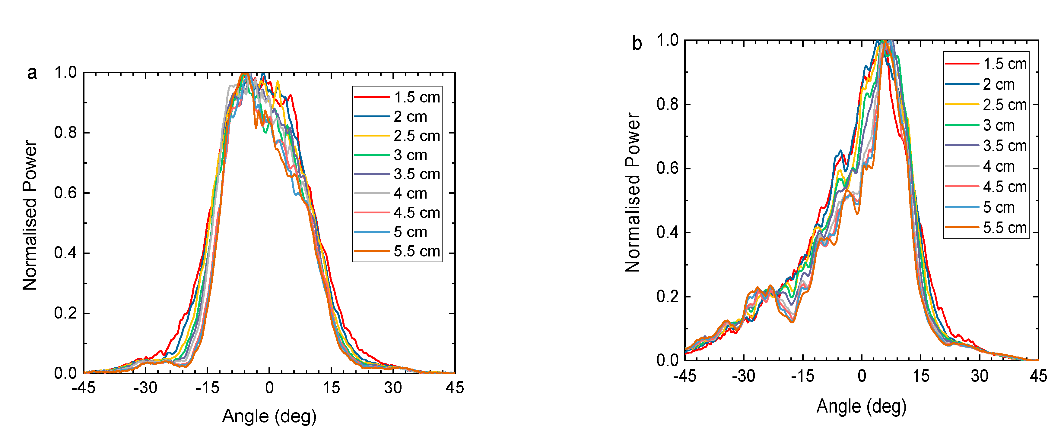
3.3.2. Dependence of Beam Profile on Distance from Detector

The validity of the angular profile measurements in this study is based on the assumption that the emitter produces a divergent beam, such that the angular profiles are distance invariant. In order to verify this assumption, angular profiles at 600 GHz were recorded at different distances from the emitter for both emitter orientations. The frequency of 600 GHz was chosen for this test and those in the following sections because at 600 GHz there is a single peak in both E-plane and H-plane, and there is sufficient THz power to provide good SNR (signal-to-noise ratio). The profiles shown in Figure 6a,b confirm good consistency, apart from minor variations in the width and height. These small features can be explained by the differences in angular resolution caused by varying the distance between the emitter and detector. The angular resolution will be discussed in detail in the next section.

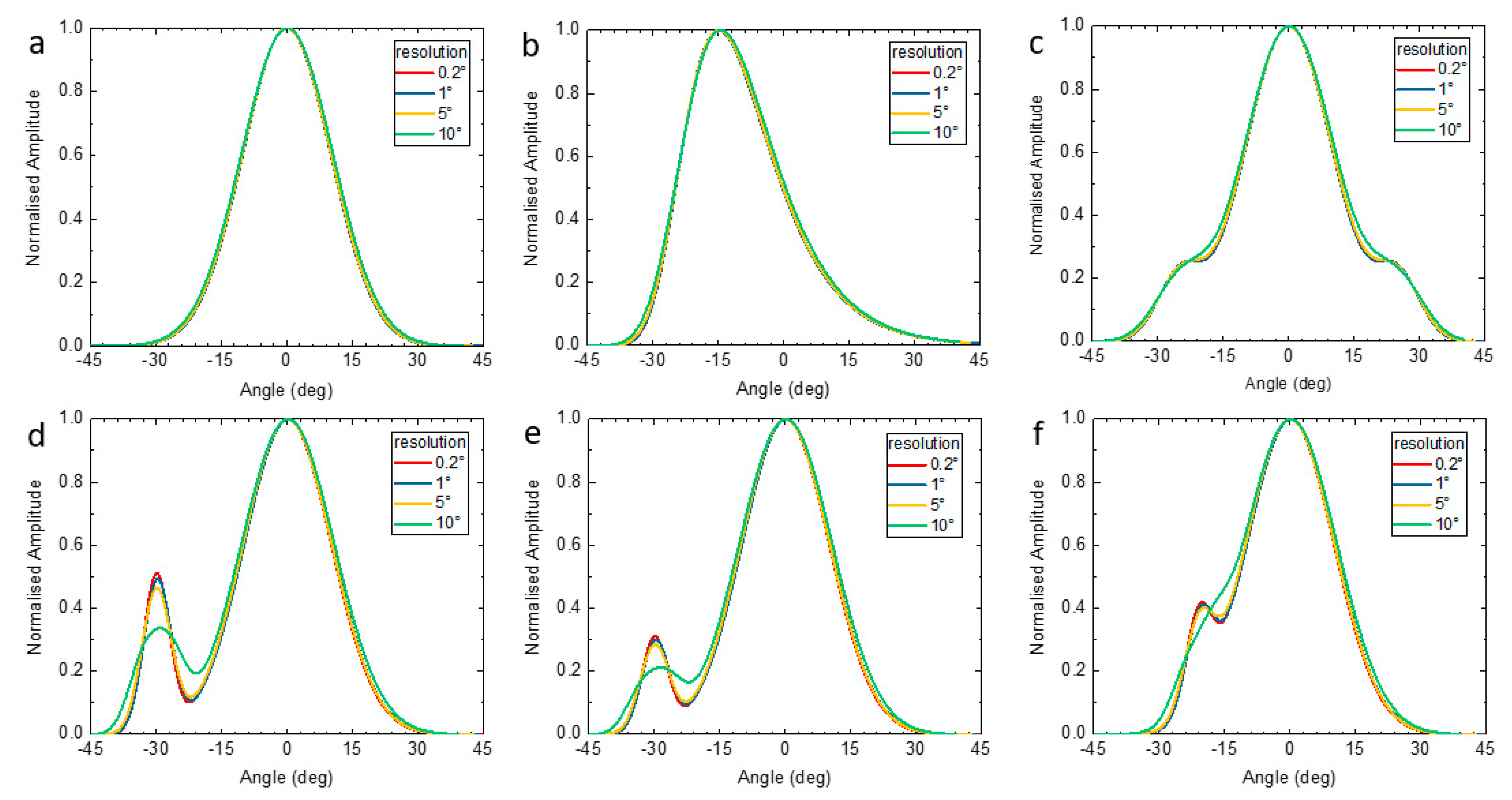
3.3.3. Angular Resolution

The step size of the rotary stage used in these measurements was 0.2°. However, as seen in Figure 2, the angular resolution θres of the measurements was limited by the diameter of the detector aperture and the distance between the emitter and detector. The aperture of the Golay detector was 11 mm and its distance from the emitter was 60 mm. Using these values, the acceptance angle of the detector is calculated to be 10.4°. To confirm this estimate, additional measurements were made at distances of 35 mm and 70 mm from the emitter, where the data at 35 mm should have an acceptance angle approximately double that at 70 mm. An extrapolation procedure was then applied to the 70 mm data to obtain an estimated profile for 35 mm, which allows to compare it with the experimental data measured at 35 mm distance. The results of this test at 600 GHz are shown in Figure 7a,b for both orientations. Both extrapolated profiles agree quite well with the measured data. Small differences in the profiles may be attributed to the aperture of the Golay being circular, whereas a square aperture was assumed in order to simplify the calculation.
Simulations of the effect of angular resolution on the observed beam profile are shown in Figure 8a–f. A variety of model beam profiles were generated with a resolution of 0.2°, including a single Gaussian, a skewed Gaussian, and Gaussians with additional lobes. These profiles were then extrapolated to show their appearance with a coarser angular resolution. The following can be concluded from these simulations:
  • In the case of a single central peak (FWHM > θres), whether a perfect (Figure 8a) or a skewed (Figure 8b) Gaussian, coarser resolution will cause negligible distortion or none, even when resolution θres is reduced by a factor of 10.
  • When narrow features are added to the curve (Figure 8c–f), then angular resolutions greater than the width of the feature (FWHM < θres) cause broadening and flattening of the feature.

3.3.4. Standing Waves

Standing waves are an important consideration in measurements of beam profiles, because they may cause errors and artefacts in the data. Standing waves are formed between the emitter and detector when their surfaces act as a resonator, supporting multiple reflections. The presence of standing waves causes significant variations in the detected signal arising from wavelength-scale changes in the relative distance between the emitter and detector. In order to understand the effect of standing waves, the beam profile at 600 GHz was mapped for both orientations over the distance equal to half-wavelength (0.25 mm). The results are shown in Figure 9a,b below. It is seen that standing waves have a negligible effect on the observed beam profile.

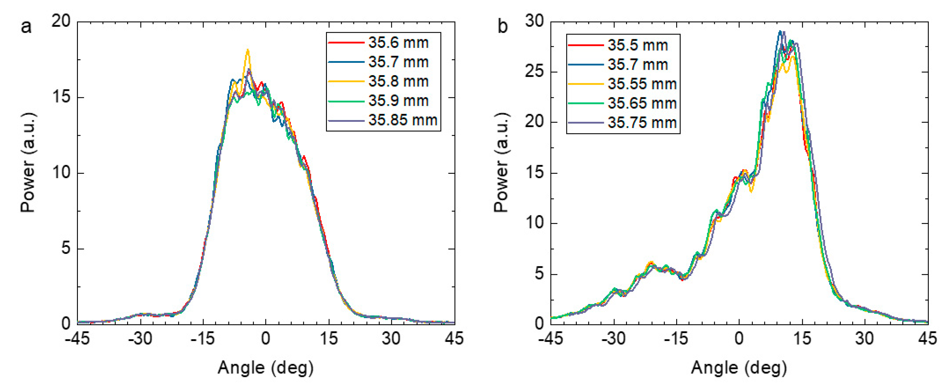
3.3.5. Repeatability of Measurements

The final experimental issue to be considered is measurement repeatability. Figure 10 shows the mean and standard deviation of five scans of the emitter at 600 GHz in the H-plane. It is seen that the noise in the data is negligible, and the error bars are too small to be distinguishable in the plot.

4. Discussion

The observed deviations in the beam profiles from a Gaussian beam may come from the coupling of the THz antenna and the Si lens [43,44,45]. It has been previously shown that small differences in the position of the lens with respect to the antenna can have significant effects on the profiles of the emitted radiation [43,44]. However, the antenna is positioned at the centre of the lens with an automated pick and place tool and the deviation from the central position is smaller than 20 µm. Hence, the effect of incorrect positioning of the chip on the lens should be of minor importance. In addition, numerical models of the beam profiles, which will be discussed in detail elsewhere, show that the emitted beam profile is expected to have a circular symmetry when the lens is perfectly centred on the emitter. However, when a small off-axis displacement (<100 μm) is present in the alignment of the lens with the centre of the emitter, both the main peak and side lobes can become asymmetrical and the main peak may become skewed. Filipovic et al. [45] showed that such a displacement can cause the peak of the radiation profile to be shifted from the centre by >10°. This type of behaviour is particularly apparent in the high frequency profiles in both orientations, as seen in Figure 4.
Internal reflections and refractions in the lens can give rise to side lobes in the beam. Although the dimensions of the silicon lens, especially the height of the hyper-hemisphere, are designed for minimal internal reflections, fabrication tolerances, which are as high as ± 50 µm, may influence the observed beam profile.
Furthermore, the features in the beam profile differ significantly between the E-plane and the H-plane, with the E-plane having more regular profiles. At lower frequencies, the features appear more pronounced. This effect is attributed to the design of the antenna structure and the feeding point geometry, which connects the diode with the bowtie antenna (see Figure 1c). The influence of the feeding point and the antenna geometry on the beam profile of PIN diode emitters is currently under further investigation.

5. Conclusions

The angular beam profiles of a THz emitter based on a PIN photodiode with attached bow-tie antenna were measured in both the E-plane and H-plane orientations at frequencies between 100 GHz and 1 THz using a Golay cell power detector. Beam profiles were recorded in the far-field of the antenna, and were found to be distance-invariant. The effects of angular resolution were examined, and it was concluded that the employed setup is capable of resolving features within 10° angular width.
For frequencies above 600 GHz, the beam profiles in the H-plane orientation were found to be significantly asymmetrical and skewed away from the centre. This may be attributed to a slight misalignment between the antenna and the centre of the lens. Moreover, the small feeding point structure that connects the photodiode and the antenna might act as a contributing radiating element and thus distort the beam profile when the wavelength becomes sufficiently small. At frequencies below 250 GHz, side lobes in the beam profiles were observed in the E-plane, and these may be attributed to internal reflections within the silicon lens.
Although some of the lower frequency profiles consist of a single peak centred around 0°, none of the measured profiles are perfectly Gaussian. This indicates the importance of acquiring accurate measurements of the radiation profiles of such emitters before considering them for use in free-space transmission systems such as those used for communications. Accurate profiles will allow for better link budget estimations in communication links. Moreover, reliable methods for beam profile measurements are essential for efficient component design. It is also important to consider the beam profile in designing optics for spectroscopy systems in order to ensure artefact-free measurements with maximum sensitivity. In addition, accurate beam profile measurements are essential for the development of broadband terahertz emitters. Hence, this paper can be an important starting point for establishing beam profile measurements as a characterization tool for terahertz emitters.

Author Contributions

Conceptualization, J.S. and M.N.; methodology, J.S., M.N., and S.N.; formal analysis, J.S. and M.N.; investigation, J.S. and M.N.; writing—original draft preparation, J.S. and S.N.; writing—review and editing, M.N., S.N., and B.G.; visualization, J.S. and M.N. All authors have read and agreed to the published version of the manuscript.

Funding

The work of J. Smith was funded by the iCASE programme of the Engineering and Physical Sciences Research Council (EPSRC), UK. The work of M. Naftaly was funded by the Horizon 2020 project “TERAPOD”, under grant agreement No. 761579. The work of S. Nellen and B. Globisch were funded by the Horizon 2020 project “TERAWAY” under grant agreement No. 871668.

Data Availability Statement

Data is contained within the article.

Conflicts of Interest

The authors declare no conflict of interest. The funders had no role in the design of the study; in the collection, analyses, or interpretation of data; in the writing of the manuscript, or in the decision to publish the results.

References

  1. Preu, S.; Döhler, G.H.; Malzer, S.; Wang, L.J.; Gossard, A.C. Tunable, continuous-wave Terahertz photomixer sources and applications. J. Appl. Phys. 2011, 109, 061301. [Google Scholar] [CrossRef] [Green Version]
  2. Wei, L.; Yu, L.; Jiaoqi, H.; GuoRong, H.; Zhang, Y.; Fu, W. Application of terahertz spectroscopy in biomolecule detection. Front. Lab. Med. 2018, 2, 127–133. [Google Scholar] [CrossRef]
  3. Yang, X.; Zhao, X.; Yang, K.; Liu, Y.; Liu, Y.; Fu, W.; Luo, Y. Biomedical Applications of Terahertz Spectroscopy and Imaging. Trends Biotechnol. 2016, 34, 810–824. [Google Scholar] [CrossRef] [PubMed]
  4. Zimdars, D.; White, J.S. Terahertz reflection imaging for package and personnel inspection. Def. Secur. 2004, 5411, 78–83. [Google Scholar] [CrossRef]
  5. Tsydynzhapov, G.E.; Gusikhin, P.A.; Muravev, V.M.; Andreev, I.V.; Kukushkin, I.V. New terahertz security body scanner. In Proceedings of the 2018 43rd International Conference on Infrared, Millimeter, and Terahertz Waves (IRMMW-THz), Nagoya, Japan, 9–14 September 2018; p. 1. [Google Scholar] [CrossRef]
  6. Trontelj, J.; Sešek, A. Electronic terahertz imaging for security applications. In Proceedings of the SPIE 9747, Terahertz, RF, Millimeter, and Submillimeter-Wave Technology and Applications IX, San Francisco, CA, USA, 13–18 February 2016; p. 974713. [Google Scholar] [CrossRef]
  7. Zhong, S. Progress in terahertz nondestructive testing: A review. Front. Mech. Eng. 2019, 14, 273–281. [Google Scholar] [CrossRef]
  8. Cosentino, A. Terahertz and Cultural Heritage Science: Examination of Art and Archaeology. Technology 2016, 4, 6. [Google Scholar] [CrossRef]
  9. Stuebling, E.-M.; Staats, N.-A.; Globisch, B.; Schell, M.; Portsteffen, H.D.; Koch, M. Investigating the layer structure and insect tunneling on a wooden putto using robotic-based THz tomography. IEEE Trans. Terahertz Sci. Technologies 2020, 10, 1. [Google Scholar] [CrossRef]
  10. Castro, C.; Nellen, S.; Elschner, R.; Sackey, I.; Emmerich, R.; Merkle, T.; Globisch, B.; De Felipe, D.; Schubert, C. 32 GBd 16QAM Wireless Transmission in the 300 GHz Band Using a PIN Diode for THz Upconversion. OFC 2019, M4F.5. [Google Scholar] [CrossRef]
  11. Ali, M.; Guzmán, R.C.; Cojocari, O.; Nellen, S.; Santamaría, G.; García-Muñoz, L.E.; Segovia-Vargas, D.; Globisch, B.; Carpintero, G. Quasi-Optic Transmitter and Receiver Modules Enabling Next-Generation Ultra-Broadband Wireless Links at Carrier-Wave Frequencies Ranging from 60 to 180 GHz. J. Infrared Millim. Terahertz Waves 2019, 40, 688–695. [Google Scholar] [CrossRef]
  12. Globisch, B.; Kohlhaas, R.B.; Liebermeister, L.; Schell, M.; Nellen, S. Recent progress of continuous-wave terahertz systems for spectroscopy, non-destructive testing, and telecommunication. In Proceedings of the Terahertz, RF, Millimeter, and Submillimeter-Wave Technology and Applications XI, San Francisco, CA, USA, 27 January–1 February 2018; Volume 10531, p. 105310C. [Google Scholar] [CrossRef]
  13. Liebermeister, L.; Nellen, S.; Kohlhaas, R.; Breuer, S.; Schell, M.; Globisch, B. Ultra-fast, High-Bandwidth Coherent cw THz Spectrometer for Non-destructive Testing. J. Infrared Millim. Terahertz Waves 2019, 40, 288–296. [Google Scholar] [CrossRef] [Green Version]
  14. Göbel, T.; Stanze, D.; Globisch, B.; Dietz, R.J.B.; Roehle, H.; Schell, M. Telecom technology based continuous wave terahertz photomixing system with 105 decibel signal-to-noise ratio and 35 terahertz bandwidth. Opt. Lett. 2013, 38, 4197–4199. [Google Scholar] [CrossRef] [PubMed]
  15. Nellen, S.; Globisch, B.; O’Gorman, J.; Anthur, A.; Vujicic, V.; Barry, L.P.; Schell, M. Fiber-coupled, photoconductive receiver for heterodyne detection up to 1 THz stabilized by an optical frequency comb. In Proceedings of the International Conference on Infrared, Millimeter, and Terahertz Waves, IRMMW-THz, Cancun, Mexico, 27 August–1 September 2017. [Google Scholar] [CrossRef]
  16. Olvera, A.F.; Lu, H.; Gossard, A.C.; Preu, S. Continuous-wave 1550 nm operated terahertz system using ErAs:In(Al)GaAs photo-conductors with 52 dB dynamic range at 1 THz. Opt. Express 2017, 25, 29492–29500. [Google Scholar] [CrossRef] [Green Version]
  17. Deninger, A.; Roggenbuck, A.; Schindler, S.; Preu, S. 2.75 THz tuning with a triple-DFB laser system at 1550 nm and InGaAs photomixers. J. Infrared Millim. Terahertz Waves 2014, 36, 269–277. [Google Scholar] [CrossRef] [Green Version]
  18. Stanze, D.; Deninger, A.; Roggenbuck, A.; Schindler, S.; Schlak, M.; Sartorius, B. Compact cw Terahertz Spectrometer Pumped at 1.5 μm Wavelength. J. Infrared Millim. Terahertz Waves 2010, 32, 225–232. [Google Scholar] [CrossRef] [Green Version]
  19. Stanze, D.; Göbel, T.; Dietz, R.; Sartorius, B.; Schell, M. High-speed coherent CW terahertz spectrometer. Electron. Lett. 2011, 47, 1292–1294. [Google Scholar] [CrossRef]
  20. Theurer, M.A.D.; Göbel, T.; Stanze, D.; Troppenz, U.; Soares, F.; Grote, N.; Schell, M. Photonic-integrated circuit for continuous-wave THz generation. Opt. Lett. 2013, 38, 3724–3726. [Google Scholar] [CrossRef]
  21. Koenig, S.C.; Lopezdiaz, D.; Antes, J.; Boes, F.; Henneberger, R.; Leuther, A.; Tessmann, A.; Schmogrow, R.; Hillerkuss, D.; A Palmer, R.; et al. Wireless sub-THz communication system with high data rate. Nat. Photon. 2013, 7, 977–981. [Google Scholar] [CrossRef]
  22. Nagatsuma, T.; Ducournau, G.; Renaud, C.C. Advances in terahertz communications accelerated by photonics. Nat. Photon. 2016, 10, 371–379. [Google Scholar] [CrossRef]
  23. Ishibashi, T.; Shimizu, N.; Kodama, S.; Ito, H.; Nagatsuma, T.; Furuta, T. Uni-Traveling-Carrier Photodiodes. In Ultrafast Electronics and Optoelectronics; The Optical Society: Washington, DC, USA, 1997; p. UC3. [Google Scholar]
  24. Bach, H.-G.; Umbach, A.; Van Waasen, S.; Bertenburg, R.; Unterborsch, G. Ultrafast monolithically integrated InP-based photoreceiver: OEIC-design, fabrication, and system application. IEEE J. Sel. Top. Quantum Electron. 1996, 2, 418–424. [Google Scholar] [CrossRef]
  25. Stanze, D.; Bach, H.-G.; Kunkel, R.; Schmidt, D.; Roehle, H.; Schlak, M.; Schell, M.; Sartorius, B. Coherent CW terahertz systems employing photodiode emitters. In Proceedings of the International Conference on Infrared, Millimeter, and Terahertz Waves, Busan, Korea, 21–25 September 2009. [Google Scholar] [CrossRef]
  26. Ishibashi, T.; Muramoto, Y.; Yoshimatsu, T.; Ito, H. Unitraveling-Carrier Photodiodes for Terahertz Applications. IEEE J. Sel. Top. Quantum Electron. 2014, 20, 79–88. [Google Scholar] [CrossRef]
  27. Nakajima, F.; Furuta, T.; Ito, H. High-power continuous-terahertz-wave generation using resonant-antenna-integrated uni-travelling-carrier photodiode. Electron. Lett. 2004, 40, 1297. [Google Scholar] [CrossRef]
  28. Renaud, C.C.; Natrella, M.; Graham, C.; Seddon, J.; Van Dijk, F.; Seeds, A.J. Antenna Integrated THz Uni-Traveling Carrier Photodiodes. IEEE J. Sel. Top. Quantum Electron. 2018, 24, 1–11. [Google Scholar] [CrossRef]
  29. Hisatake, S.; Kim, J.-Y.; Ajito, K.; Nagatsuma, T. Self-Heterodyne Spectrometer Using Uni-Traveling-Carrier Photodiodes for Terahertz-Wave Generators and Optoelectronic Mixers. J. Light. Technol. 2014, 32, 3683–3689. [Google Scholar] [CrossRef]
  30. Rouvalis, E.; Fice, M.J.; Renaud, C.C.; Seeds, A.J. Optoelectronic detection of millimetre-wave signals with travelling-wave uni-travelling carrier photodiodes. Opt. Express 2011, 19, 2079–2084. [Google Scholar] [CrossRef] [PubMed] [Green Version]
  31. Rouvalis, E.; Renaud, C.C.; Moodie, D.G.; Robertson, M.J.; Seeds, A.J. Continuous Wave Terahertz Generation From Ultra-Fast InP-Based Photodiodes. IEEE Trans. Microw. Theory Tech. 2012, 60, 509–517. [Google Scholar] [CrossRef]
  32. Van Rudd, J.; Mittleman, D.M. Influence of substrate-lens design in terahertz time-domain spectroscopy. J. Opt. Soc. Am. B 2002, 19, 319–329. [Google Scholar] [CrossRef]
  33. Nellen, S.; Ishibashi, T.; Deninger, A.; Kohlhaas, R.B.; Liebermeister, L.; Schell, M.; Globisch, B. Experimental Comparison of UTC- and PIN-Photodiodes for Continuous-Wave Terahertz Generation. J. Infrared Millim. Terahertz Waves 2019, 41, 343–354. [Google Scholar] [CrossRef] [Green Version]
  34. Balanis, C.A. Modern Antenna Handbook, 4th ed.; John Wiley & Sons: Hoboken, NJ, USA, 2011. [Google Scholar]
  35. Han, J.W.; Choi, Y.G.; Lee, J.S. Radiating pattern of surge-current-induced THz light in near-field and far-field zone. Sci. Rep. 2018, 8, 6513. [Google Scholar] [CrossRef] [Green Version]
  36. Damian, V.; Vasile, T. Techniques for THz Beams Evaluations; CAS: Sinaia, Prahova, 2017; pp. 227–230. [Google Scholar] [CrossRef]
  37. Logofătu, P.C.; Damian, V. Super resolution terahertz imaging by subpixel estimation: Application to hyperspectral beam profiling. J. Opt. 2018, 20, 055701. [Google Scholar] [CrossRef]
  38. Bitzer, A.; Helm, H.; Walther, M. Beam-Profiling and Wavefront-Sensing of THz Pulses at the Focus of a Substrate-Lens. IEEE J. Sel. Top. Quantum Electron. 2008, 14, 476–481. [Google Scholar] [CrossRef]
  39. Richter, H.; Greiner-Bär, M.; Pavlov, S.G.; Semenov, A.D.; Wienold, M.; Schrottke, L.; Giehler, M.; Hey, R.; Grahn, H.T.; Hübers, H.-W. A compact, continuous-wave terahertz source based on a quantum-cascade laser and a miniature cryocooler. Opt. Express 2010, 18, 10177–10187. [Google Scholar] [CrossRef]
  40. Steiger, A.; Gutschwager, B.; Kehrt, M.; Monte, C.; Müller, R.; Hollandt, J. Optical methods for power measurement of terahertz radiation. Opt. Express 2010, 18, 21804–21814. [Google Scholar] [CrossRef] [PubMed]
  41. Vasile, T.; Damian, V.; Coltuc, D.; Petrovici, M. Single pixel sensing for THz laser beam profiler based on Hadamard Transform. Opt. Laser Technol. 2016, 79, 173–178. [Google Scholar] [CrossRef]
  42. Balanis, C.A. Antenna Theory: Analysis and Design; John Wiley & Sons: Hoboken, NJ, USA, 2016. [Google Scholar]
  43. Ozbey, B.; Sertel, K. Distinct Gaussian Properties of Multiple Reflections in Extended Hemispherical Lenses. J. Infrared Millim. Terahertz Waves 2019, 40, 1053–1073. [Google Scholar] [CrossRef]
  44. Jepsen, P.U.; Keiding, S.R. Radiation patterns from lens-coupled terahertz antennas. Opt. Lett. 1995, 20, 807–809. [Google Scholar] [CrossRef]
  45. Filipovic, D.; Gauthier, G.; Raman, S.; Rebeiz, G. Off-axis properties of silicon and quartz dielectric lens antennas. IEEE Trans. Antennas Propag. 1997, 45, 760–766. [Google Scholar] [CrossRef]
Figure 1. (a) Photograph of the fibre-coupled PIN-PD emitter module. Optical fibre (blue cable) and SMB cable (black cable) for the electrical bias can be seen. (b) The H- and E-plane orientations are marked on the housing of the module. (c) Schematic structure of the PIN-PD emitter chip. The waveguide integrated PD is connected to an extended bow-tie antenna with a bracket-like electronic structure (inset). H- and E-field orientations are highlighted.
Applsci 11 00465 g001
Figure 2. Experimental set-up for mapping angular beam profiles. The source, mounted on a rotary stage, is rotated between −45° and 45° with respect to the detector. The detector is placed on a linear translation stage to allow variation of the distance between the emitter and detector.
Applsci 11 00465 g002
Figure 3. (a) Power output of the PIN diode as a function of frequency. Power was measured with a calibrated pyroelectric detector for frequencies below 500 GHz and with a Golay cell for 200 GHz to 1000 GHz. (b) Optical setup for power measurement.
Applsci 11 00465 g003
Figure 4. Normalized angular beam profiles of the PIN diode emitter for frequencies between 100 GHz and 1 THz at 50 GHz intervals, measured at a distance of 60 mm from the emitter for: (a) H-plane orientation and (b) E-plane orientation. All profiles are normalised for ease of comparison.
Applsci 11 00465 g004
Figure 5. The far field distance, as given by Equation (2), for frequencies between 100 GHz and 1 THz for radiation travelling through air and silicon.
Applsci 11 00465 g005
Figure 6. Beam profiles measured at varying distance between the emitter and the detector, at 600 GHz for: (a) E-plane orientation and (b) H-plane orientation.
Applsci 11 00465 g006
Figure 7. Comparison of the profile at 600 GHz measured at 35 mm from the emitter with an acceptance angle of 17.9° with the profile extrapolated from a measurement at 70 mm from the emitter with an acceptance angle of 9.0°: (a) E-plane orientation and (b) H-plane orientation.
Applsci 11 00465 g007
Figure 8. Simulations of model beam profiles as they would appear at various acceptance angles, revealing the effects of angular resolution. The initial profile has 0.2° resolution. (a) single Gaussian, (b) skewed Gaussian, (c) Gaussian with shoulders, (df) Gaussian with additional 3° wide feature of differing amplitudes and separation.
Applsci 11 00465 g008
Figure 9. Comparison of beam profiles at 600 GHz measured at various positions on a standing wave. (a) E-plane orientation where 35.6 mm and 35.9 mm are at the wave maximum. (b) H-plane orientation where 35.5 mm and 35.75 mm are at the wave maximum.
Applsci 11 00465 g009
Figure 10. The mean and standard deviation of 5 beam profile scans at 600 GHz in the H-plane orientation. The error bars are shown in pink.
Applsci 11 00465 g010
Publisher’s Note: MDPI stays neutral with regard to jurisdictional claims in published maps and institutional affiliations.

