1. Introduction
The popularity of the matrix converter increased in the last years [
1,
2] due to the possible advantages over the standard back-to-back converters (BBC). The improvement in the semiconductor industry, especially in the field of Silicon Carbide (SiC) and Gallium Nitride (GaN) transistors and the small footprint of the component, has opened new ways to build a compact and high-power density matrix converter. The main advantage of the matrix converter is the absence of the storage components (capacitor or inductor), which are getting bulkier if the output power of the standard BBC converter rises. The lack of storage components predetermines the matrix converter to applications with high-power density and it can be used in environments with low or high temperatures (for example, in aerospace applications). The market research shows that commercial products are not available nowadays for use in the matrix converter application. In the past, some power modules were designed and introduced. However, they are not available now due to the shortage of products, and researchers must design their module for the direct matrix converter (DMC) or indirect matrix converter (IMC). For the proper function of the converter, a bidirectional switch is required. The bidirectional switches are built from the discrete transistor in various configurations shown in
Figure 1.
The first device is built from one semiconductor switch and four diodes, where the diode bridge is used. The advantage is that no complex commutation algorithm is required. The main disadvantage is the higher power losses, since the load current flows through three semiconductor devices [
3]. The second configuration in
Figure 1b, called the common emitter, is widely used due to its good dynamic parameters and lower power losses in comparison to the connection in
Figure 1a [
3]. The switch in
Figure 1c is, from the loss point of view, the same as in
Figure 1b but requires less isolated power supplies in the case of a 3 × 3 converter [
3,
4]. The CC-switch configuration requires six power supplies, and the CE-switch configuration requires nine power supplies. The CC configuration has worse dynamic parameters due to the big collector parasitic inductance of the components [
1]. The last structure is shown in
Figure 1d and is represented by the RB-IGBT, which can block voltages in the reverse direction. However, their dynamic behavior in reverse recovery is very slow compared to the standard P-N diode, which can significantly raise the power losses. Because of the slow reverse recovery behavior, these types of switches are not much used in this application currently [
5]. The experiments with the relatively new GaN technology show the potential of this technology to be used in future matrix converters applications [
6,
7,
8,
9].
These publications show the effort of the researchers to build a compact sample of the bidirectional switch for the matrix converter [
10], where authors build an intelligent power switch module with implemented commutation in the module (since every module consists of a microcontroller in which the commutation algorithm is implemented). The next publications show a sample of the low parasitic inductance module based on the SiC chips from the CREE manufacturer [
11,
12]. The disadvantage of these modules is that if one device is destroyed, the whole module becomes useless, or the replacement of the broken component can be very expensive. A partial solution is presented in [
13], where authors used D2PAK IGBTs mounted at the PCB in 3 × 1 configuration. This arrangement ensures good maintenance and reparability, but using the IGBT transistor leads to higher power losses which cannot be easily dissipated through FR4 substrate. So, additional cooling is required, especially at higher power outputs. Another approach presented by the authors in [
14] offers a compact direct matrix converter using the SiC MOSFETs. The sample with a power of 2 kW was built in the PCB with dimensions of 358 × 155 × 40 mm. The high-density sparse matrix converter is presented in [
15] with a very compact design wherein SiC MOSFETs were used. The power output of the converter is 1500 W, and the demonstrated power losses by the authors are below 80 W with a switching frequency of 100 kHz.
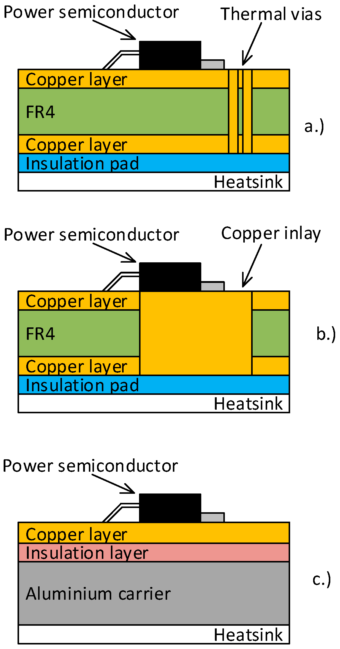
Several methods for cooling high-power surface mount technology (SMT) components are described in [
16,
17], as well as the impact of the vias placement on the cooling performance [
18]. The first uses the thermal vias in the two-layer or multilayer PCB as shown in
Figure 2a. The generated heat is dissipated through vias to the heatsink or the inner layers of the PCB. This method needs an additional insulating heat-conducting pad between the FR4 substrate and heatsink to ensure the right insulation of the board if high voltage is present. The next approach shown in
Figure 2b, which can reach potentially lower thermal resistances, is PCB with copper inlays. This method is attractive from the low thermal resistance point of view but faces the same insulation problem. Additionally, non-standard manufacturing technology must be used, which can be costly, especially in small batches. The next solution on the market is the insulated metal substrate (IMS) boards, shown in
Figure 2c, which ensure a good thermal interface between the SMT component and the heatsink with low thermal resistance provided by the metallic core. These PCBs are widely used in the automotive industry due to their good performance in the cooling of power LED modules. If electrical insulation is needed, manufacturers can offer IMS boards with an insulation voltage up to 4 kV. According to the datasheet of the used IMS board with the market name Goldenmax G11, the breakdown voltage is above 3 kV, declared by the manufacturer.
This paper focuses on the design, modeling, and practical realization of the 3 × 1 matrix converter module, with easy expandability to provide a matrix converter with various input/output configurations. According to the authors’ research, no modules with similar parameters are now commercially available. The presented module can deliver power up to 1.7 kW. The designed module is part of the research project for the control of multiphase drives and the investigation of converter efficiencies. In the five-phase application, the presented modules in this configuration can deliver up to 8.5 kW. The output power of the module is adjustable by the change of power semiconductors and can be increased up to 3.5 kW per module.
2. Structure of the Module
The module was designed to be very compact, considering the mounting of almost all required components to drive the module, with only the need for external signals to control the module. Due to this consideration, the design was separated into three parts. The block diagram with the highlighted blocks is shown in
Figure 3.
For the power part, the SiC transistors were used due to their relatively high operation temperature, high blocking voltage, and relatively small form factor. Recently, the ON-Semiconductors manufacturer released a new family of the SiC MOSFETs, which were well suited for this application. The semiconductors are in the D2PAK-7 package with a Kelvin source pin extended from the package to ensure proper driving of the device. It is important to select the right mounting of the semiconductors to ensure good electrical insulation and good heat dissipation. For this application, the best price to performance ratio is achieved by the IMS boards according to the research in the introduction. Additionally, this approach does not need an insulating pad between PCB and the heatsink, increasing thermal resistance significantly.
For the power part, the common-source configuration of the switches was selected. As described in many publications [
19,
20,
21,
22,
23,
24], the commutation algorithm must be implemented to ensure no short or open circuit development, leading to overvoltage and overcurrent generation and circuit destruction. Many commutation techniques are available where most of them are based on the output current measurement. Thus, the authors decided to implement a current direction measurement to the power board for the commutation investigation in future work. The output current direction in the matrix converter can be measured in many ways, and these methods are summarized in
Table 1, together with possible advantages and disadvantages.
Since the current direction detection circuitry is designed at the power IMS board, the authors selected a method that measures at the output diodes, offering good precision and fast reaction. The power losses can be effectively dissipated through the metal board to the heatsink. If the diodes with low drop voltage are selected, the power losses can be reduced significantly. The circuit is supplemented with the fast comparator to detect the voltage drop direction at the diodes, as shown in
Figure 4. The board was designed to one-layer IMS board with final dimensions of 129 × 58 mm. The design of the power board is shown in
Figure 4. The board consists of four mounting holes to be easily mounted to the heatsink.
The design of this board allows the change of the power devices based on the output power specification of the matrix converter. The 3D model of the power board is shown in
Figure 5.
The second board was designed for driving SiC transistors. The SiC transistors offering a high blocking voltage together with a low R
DS(on) in comparison with traditional MOSFET technology. To ensure the short signal traces to the SiC MOSFET Gate pin, the driver board is placed right above the power board. The signals are transferred through the connectors. Since the input of the converter is connected to the phase voltage and a common source of transistors floats at the high voltage potentials, the isolated gate driver is needed. For the proper supply of the secondary side of the driver, the isolated push-pull power supply is designed based on the SN6505 push-pull driver to ensure a small form factor. The secondary voltage from the power supply is 18.5 V, and this voltage is further divided into +15.5 V and −3 V to ensure proper driving of the SiC power MOSFETs. For the gate driving, the dual isolated gate driver for the H-bridge applications was used. The secondary side of this driver was designed that way so that this driver can drive two transistors connected with a common source. The driver is capable of sourcing 4 A and sinking 6 A to each MOSFET. For proper SiC driving and ensuring that the driver is not overloaded by the current, the proper external gate resistors must be selected as shown in
Figure 6. The following driving configuration was selected to ensure faster gate discharge and thus faster turn off times:
During the turn-on, only the
RON resistor applies, since diode
D is in the blocking direction. In the turn-off time, the diode is in the conducting stage and the resistors are connected in parallel, which allows reaching a higher discharge current. The resistors were selected as follows:
RON = 4.1 Ω and
ROFF = 2.8 Ω. Then, the current capacity of the driver needs to be checked [
25]:
where
ROH and
ROL represent internal driver driving MOSFETs resistances,
RNmos is internal pull-up driving resistor, and
RON,
ROFF, and
RFETin represent the turn-on, turn-off, and SiC internal resistors, respectively, according to the SiC datasheet. Diode forward voltage is represented by
VD and supply voltages are denoted in
VDD for positive rail and
VSS for negative rail. The calculated values from (1) and (2) must be lower than 4 A for turn-on current (
IPOS_MAX) and lower than 6 A for turn-off current (
INEG_MAX) according to datasheet [
25], to ensure that driver is not overloaded. In our case, the calculated results are 2.9 A and 5.2 A for
IPOS_MAX and
INEG_MAX, respectively. Calculated values are below the maximum values specified by the datasheet [
25] which confirms the correctness of the design. All circuitry in the driver board is powered from the single 5 V power supply. The board includes a voltage supervisor IC, which ensures the power supplies startup when the supply voltage reaches 4.7 V by enabling the drivers to prevent current inrush.
Together with isolated power supplies and isolated gate drivers, the current measurement was implemented on this board. Current measurement is implemented on the driver board (Top PCB). The OUT pin shown in
Figure 4 and
Figure 5 is used to conduct current from the power board to the driver board. Then, the current is flowing through the hall current sensor and then to the output phase pin shown in
Figure 7. The sensor can measure current in the range of
± 20 A, which is suitable for this application, even if the SiC devices would be changed for more powerful ones. If the output current would be bigger, the manufacturer of the sensor offers a
± 30 A version in the same package, which can be easily changed if more output power is needed. Finally, the board involves a high-speed optocoupler, which ensures galvanic isolation and transfers the direction of the output current flowing through the module. The designed driver board is shown in
Figure 7.
The power and driver board are stackable with one another. The signal connections are made through pin headers. The connection of power high-voltage lines is made through steel-tinned standoffs. On the power board, the standoffs are soldered directly to the board, and in the driver board, the mounting screw is used. The assembled 3D model of the power and driver board is shown in
Figure 8.
Due to the space limitations on the driver board, the input signal board shown in
Figure 2 must be designed on the separated PCB. This board consists of a buck power supply with an operating range from 9 V to 15 V and output power of 10 W. For the interface, three different connectors are used. For the pulse width modulation (PWM) signals, the RJ50 shielded connector is used. This connector transfers six PWM signals, and the remaining wires are used as supply voltage lines. The level shifter shifts input PWM signals to the 5 V level appropriate for the gate drivers. For the current direction and the actual measured current value, the RJ11 connector is used. The value of the output module current is transferred through the differential twisted pair to improve immunity to electromagnetic interference. Finally, the optical TOS-LINK connector is added to the board. Through this interface, the current direction is transmitted too so that the board can transmit the current direction signal in two ways. The optical interface is fast, reliable, and immune to electromagnetic interference, so it is preferred in a disturbed environment. The signal board is mounted perpendicularly to the driver board, so all connectors face upwards. The 3D model of the assembled 3 × 1 matrix converter module is shown in
Figure 9.
For further protection against the accidental touch of the high voltage connectors, the cover was designed. The finalized module with the designed cover can be seen in
Figure 10.
The final dimensions of one 3 × 1 matrix module are 130 × 54 × 43 mm (length × width × height). All PCBs were manufactured, and the final module was assembled according to designed 3D models.
3. Verification of the Operation
For the proper SiC MOSFETs driving, the isolated power supply must be capable of delivering at least 1 W of the power. The output power of the isolated power supply was measured together with an output voltage as a load current function. The efficiency was calculated from the measured data. The measured data of the power supply are shown in
Figure 11.
As shown in
Figure 11, the operating output power of approximately 1 W to 2 W converter reaches its maximum efficiency of around 82%. The converter can deliver more power in case if more powerful semiconductors are used. The output current is limited to 200 mA due to the used secondary rectification diode limitation. The thermal image of the one power supply during the output load of 2 W can be seen in
Figure 12.
After the power supply efficiency and maximum load temperature, the most important indicator of the power supply quality is the output voltage waveform, especially during the startup of the power supply and dynamic events. If the overvoltage occurs during the startup, this can lead to the destruction of the semiconductor components. Thus, measuring the quality of the output waveform is important. The waveform of all of the voltages during the converter power supplies startup sequence can be seen in
Figure 13.
The Input signal represents the 12 V supply rail provided by the laboratory power supply. The 5 V rail is measured at the output of the buck converter. The Enable signal represents the signal from the supervisor circuit monitoring the 5 V rail. Finally, the Isolated signal is the voltage at the secondary side of the isolated power supply for the gate drivers. As shown in
Figure 13, no overshoots are present, and the startup of the isolated power supply occurs after enabling signal when the 5 V supply rail is present and stable.
For the driver functionality verification, the PWM signal was applied to the input of the driver board, and the output signal was measured at the gate of the SiC MOSFET. The measured waveforms can be seen in
Figure 14.
The cyan waveform in
Figure 15 represents the output signal applied to the SiC MOSFET gate, where turn-off is represented by the −3 V and turn-on is represented by the +15 V, as was designed. In the isolated gate driver, the important parameter is the signal propagation delay from the non-isolated to the isolated side. The measured value of delay was 20 ns for the turn-on waveform and 25 ns for the turn-off waveform. These measured values correspond to the values in the driver datasheet.
One important aspect of the gate driver circuitry is the stability and the response of the isolated power supply. During the turn-on and turn-off process, the major current needs to be delivered or removed from the MOSFET gate. These currents are delivered mainly from the isolated power supply capacitors, and when the switching state is stable, the capacitors are recharged. If the voltage drop during the turn-on or turn-off transients is big, this can lead to a faulty transistor switch or can cause triggering under-voltage protection in the modern gate driver ICs. In this case, the single power supply needs to deliver the required power to the two transistors since the switch is bidirectional and constructed from two SiC devices connected by the common source. Measurement of the stability of the positive supply rail during turn-on and turn-off can be seen in
Figure 16.
As can be seen in
Figure 16, the power supply recovery from the turn-on transient last below 20 ns, with a negative overshoot of 1 V. For the turn-off process, the transient last below 50 ns with a positive overshoot of 1.9 V. At the end of turn-on or turn off process, the power supply rail is stable again.
In the next measurement, the output current detection circuit was measured. The isolated autotransformer was used to generate the AC waveform. The load for the AC waveform was a 33 Ω power resistor. The voltage oscilloscope probe measured the output of the current detector circuit, and the output current of the module was measured using a current probe (Tektronix TCP303). The current measurement designed at the board was evaluated too. The output of this sensor is the differential pair which represents the flowing current through a circuit. Differential output was selected due to its very high resistance to the surrounding interface. The measured results are shown in
Figure 17.
As shown in
Figure 17, the current detection circuit measures the direction of the output current reliably. The cyan and purple waveforms represent the differential outputs from the current value measurement circuitry. The signals are measured against the ground. For better visualization of the current detector functionality, the waveforms were measured with the same position settings, as shown in
Figure 18.
The manufactured power board on the IMS with all power semiconductors assembled can be seen in
Figure 19 at the left image. The top three spacers are used as connectors for input phases. The bottom two spacers are used as mounting and fixing supports for the higher rigidity of the module. The spacer mounted at the right side is the output phase connected to the driver board, where the current of this phase is measured. The assembled power board and the driver PCB can be seen in
Figure 19 at the right side image.
The designed cover for the compact matrix module presented in
Figure 9 was tested too. The design was manufactured with the help of a 3D printer. The cover provides additional protection against accidental contact with the live parts of the module. The assembled module with the cover can be seen in
Figure 20.


