Abstract
A systematic analysis of the performance of VCSELs, fabricated with a decreasing number of structural elements, is used to assess the complexity of fabrication (and therefore time) required to obtain sufficient information on epitaxial wafer suitability. Initially, sub-mA threshold current VCSEL devices are produced on AlGaAs-based material, designed for 940 nm emission, using processing methods widely employed in industry. From there, stripped-back Quick Fabrication (QF) devices, based on a bridge-mesa design, are fabricated and this negates the need for benzocyclcobutane (BCB) planarisation. Devices are produced with three variations on the QF design, to characterise the impact on laser performance from removing time-consuming process steps, including wet thermal oxidation and mechanical lapping used to reduce substrate thickness. An increase in threshold current of 1.5 mA for oxidised QF devices, relative to the standard VCSELs, and a further increase of 1.9 mA for unoxidised QF devices are observed, which is a result of leakage current. The tuning of the emission wavelength with current increases by 0.1 nm/mA for a VCSEL with a 16 μm diameter mesa when the substrate is unlapped, which is ascribed to the increased thermal resistance. Generally, relative to the standard VCSELs, the QF methods employed do not significantly impact the threshold lasing wavelength and the differences in mean wavelengths of the device types that are observed are attributed to variation in cavity resonance with spatial position across the wafer, as determined by photovoltage spectroscopy measurements.
1. Introduction
Vertical cavity surface emitting lasers (VCSELs) have become ubiquitous in recent years due to their use as light sources in a wide range of applications from 3D imaging to optical fibre data transmission and, with the emerging technology of LiDAR, the market is rapidly expanding [1,2,3,4]. This expansion has led wafer manufacturers to scale up production to larger substrates; currently 6-inch (152 mm) [5] and beyond [6], whilst work is also being done to maximise the uniformity over individual wafers, as well as between wafers from the same and separate growth runs. This relies on material characterisation methods that are compatible with a commercial manufacturing process, that is, rapid time-to-result with representative information output. This is typically managed with non-destructive wafer characterisation techniques such as defect scanning [7] and measurement of the reflectivity spectrum for information on the resonant wavelength of the VCSEL stack [8]. Destructive techniques such as capacitance-voltage measurements on etched VCSEL material to validate doping levels [9] and secondary ion mass spectroscopy to measure material compositions [10] are employed on sacrificial wafers. Photoluminescence spectroscopy is also often used to obtain information on quantum well (QW) layers [11], but this involves growth of a test structure or removal of the top DBR from the full VCSEL material, which is less representative of the full structure.
Ultimately, these methods of wafer characterisation aim to provide information that is used to predict yield and the final performance of fabricated VCSEL devices. Often, some VCSELs are fabricated from calibration material for light-current-voltage (L-I-V) and wavelength (λ) measurements to supplement the material characterisation. The information revealed is extremely valuable, but this can prove to be a time-consuming process. Here, we report on the development of a Quick Fabrication (QF) VCSEL test structure, that will enable epitaxial material to be characterised based on laser performance. Key figures of merit from the laser characterisation can be mapped across a wafer in the same way as commercial-standard measurements, but here we seek to assess the physical impact of a simplified (and therefore more rapid) fabrication process on performance for devices relative to typical VCSELs.
In this work, we focus on VCSELs produced on AlGaAs-based epitaxial material designed for 940 nm emission wavelengths. Infrared emitting VCSELs have been widely shown to have low threshold currents resulting from a combination of advances in epitaxial design and improved processing [12,13,14,15,16], but the threshold current of a VCSEL is highly dependent on the size of the active area [17] and the particular device structure. Thus, we assess the size-dependent threshold current for the devices produced in this study and use this as a useful way to compare different design variations.
Additionally, improved output powers have been achieved by rethinking the design and packaging of the VCSELs [18] and high single-mode output powers have been achieved at this emission wavelength by employing Zn-diffusion in the fabrication process [19,20]. However, here, we are concerned only with top-emitting oxide-confined VCSELs. The optical power of VCSELs has been shown to increase with increasing active diameter [21,22], but this has also been seen to saturate for large devices [23] and with increasing internal heating [24]. The optical power of the QF devices and the dependence on device size is examined in this study and a comparison of the relative efficiencies of the different designs is made.
Further, VCSELs inherently operate at a single longitudinal mode due to the standing wave pattern formed by the epitaxial structure [25,26] and, unlike edge-emitting lasers, the emission wavelength of a VCSEL is determined by the material cavity resonance, as opposed to the wavelength corresponding to peak gain. As a result, the emission wavelength is relatively stable but does shift with increasing temperature, with the rate of shift determined by the change in refractive index of the constituent materials [27,28,29]. The emission wavelength is also observed to redshift with increasing current [26,30] as a result of internal heating. Thus, measurement of the dependence of the emission spectrum on injection current is a useful tool to assess the self-heating properties of devices and is employed in this work to compare the various device types.
2. Materials and Methods
The epitaxial structure used in this study consists of a multiple quantum well active region sandwiched between upper p-doped and lower n-doped GaAs/AlGaAs distributed Bragg reflector (DBR) mirror pairs and is designed for 940 nm emission wavelength. A high aluminium content layer was included between the upper DBR and above the confinement layers of the active region for definition of the VCSEL aperture. The epi-structures were grown via MOCVD on n+ GaAs substrates and provided by IQE plc.
Devices from several variations on a quick fabrication process were compared with the performances of typical commercial-standard VCSELs, which we refer to as standard VCSELs. The QF structures were based on an etched-trench bridge-mesa design, whereby the central cylindrical VCSEL cavity is not fully isolated from the surrounding planar material.
The remaining material is referred to as the bridge, as this facilitates deposition of a bond pad in the same plane as the p-metal ring contact without the need for a planarisation process step. A SEM image of a QF VCSEL mesa is shown in Figure 1a, with that of a standard VCSEL in Figure 1b.
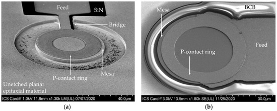
Figure 1.
(a) SEM Image of a Quick Fabrication (QF) VCSEL; (b) SEM image of a standard VCSEL.
Fabrication followed common processing techniques which, for the standard VCSEL structures was as follows: definition of the mesa by inductively coupled plasma (ICP) etch to just below the active layers, a depth of ~3 μm. Wet thermal oxidation of the samples at 400 °C to form the oxide apertures with an oxidation depth of 5.5 0.5 μm. The samples were spin-coated with benzocyclcobutane (BCB) and subsequently etched-back to planarise the material to the height of the mesas. Ti/Au (10/500 nm) p-metal ring contacts and bond pads were deposited simultaneously on the top of the samples, followed by standard AuGe/Ni/Au deposition for the global substrate-side n-metal contact.
The process for the Quick Fabrication VCSELs was as follows: a blanket-coat of 200 nm SiN was deposited and used as the etch mask for definition of the mesa by inductively coupled plasma (ICP) etch, as was done for the standard VCSELs. Here, though, the SiN was patterned to be used as an insulating layer to prevent electrical pumping underneath the bond pad, given that the mesas were not fully isolated. The samples were oxidised in the same conditions as for the standard VCSELS, but for a total oxidation length of 12 μm. The deposition for the top p-metal and substrate-side n-metal layers were the same as for the standard VCSELs. However, prior to the deposition of the n-contact, the substrate of some samples was mechanically lapped, thinning the substrate from 600 μm to approximately 150 μm, followed by a polishing process. While substrate thickness is usually reduced for ease of die singulation, for the purpose of testing QF VCSELs this step is not a necessary requirement; here, the effect of removing this step is carried out to understand the impact on device performance.
Light-current-voltage measurements were performed on a range of device sizes using a CW current source with an integrating sphere for light collection and power measurement. Spectral () measurements were done by coupling light into an optical spectrum analyser (resolution 0.1 nm) using a focusing lens and multimode fibre connect.
The VCSELs were mounted on a temperature-controlled stage to facilitate temperature dependent measurements between 23 and 80 °C. Near-field images for the devices were obtained using a focusing lens to collect light which was then detected with a CCD camera. More time-consuming measurements, such as wavelength variation with current and temperature, were performed on a reduced number of devices based on L-I-V-λ screening. Additionally, surface photovoltage spectroscopy (SPVS) [31,32,33] was used to measure the cavity mode wavelength of the epi-material. SPVS involves shining wavelength-varied monochromatic light normal to the surface of the sample and measuring the voltage induced as photogenerated electron-hole pairs are separated by the built-in field.
3. Results and Discussion
3.1. Threshold Current
We begin by analysing the performance of the full VCSEL structures, which is used as a baseline from which we compare the performance of the less complex QF device structures.
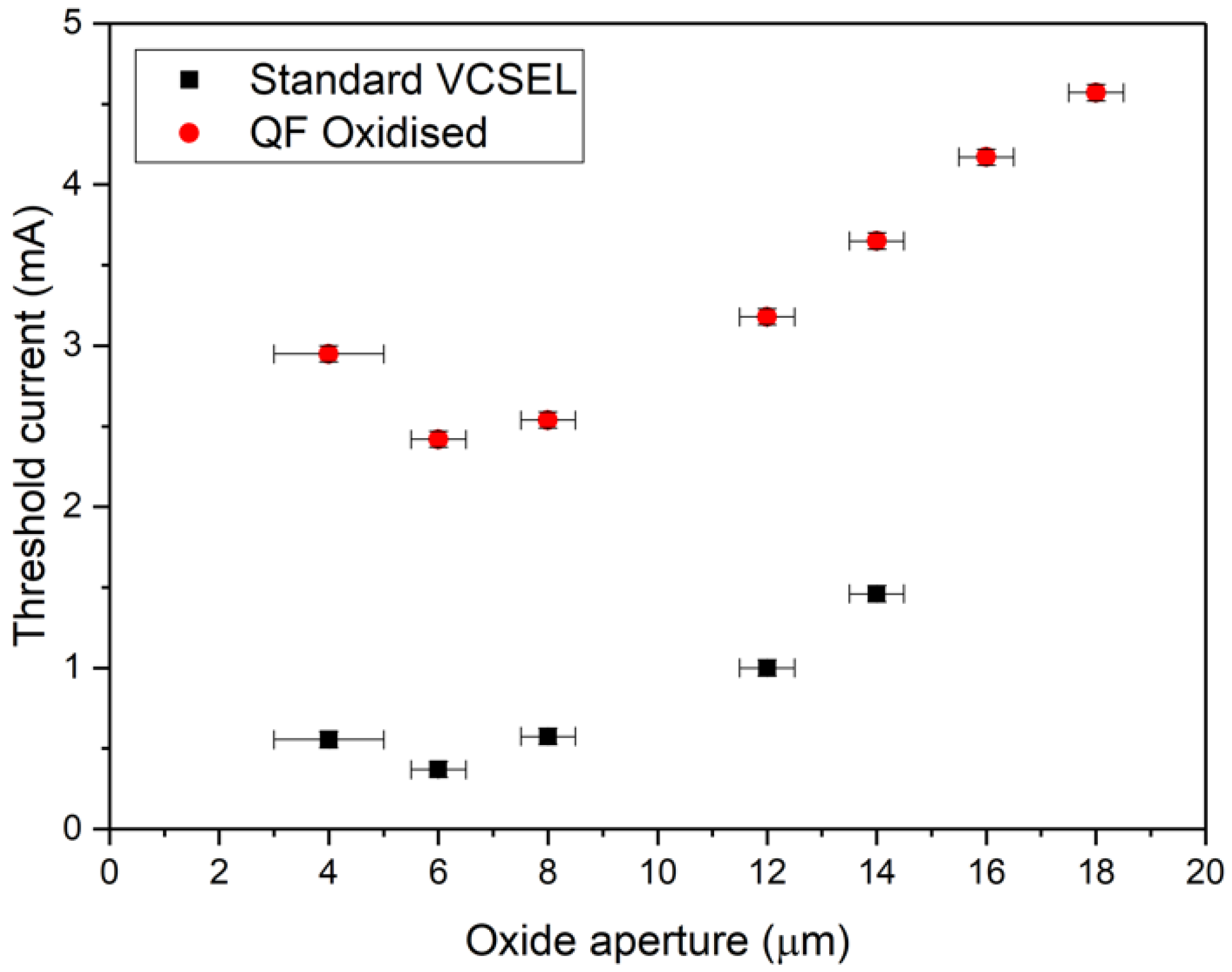
Threshold currents were found to be sub-mA for devices <10 μm diameter oxide aperture. Threshold currents for the complete set of devices ranged between 0.37 and 1.46 0.01 mA for 6–12 μm apertures. The threshold currents quoted in this work were extracted from L-I curves by the second-derivative method and the uncertainty quoted is determined by the resolution of the current source and applies to all threshold current values presented here. It is well known that the threshold current of a diode laser scales with increasing active volume [17], and this is shown in Figure 2 for these VCSEL structures, where the uncertainty in the aperture is due to the resolution of the measurement of the oxidation extent under an infrared camera. The rate of oxidation increases as the device size reduces, hence there is a greater uncertainty in the aperture diameter for the smallest mesas. Additionally, for a 4 μm aperture device, we see an increase in threshold current to 0.60 mA. This has been explained previously by an increased internal optical loss due to scattering at the oxide layers for small apertures [34,35,36], greater sidewall recombination as device diameter is reduced [17,37,38] and an increased internal temperature [28,39,40] driven by the increased series resistance of small aperture devices. The threshold currents for oxidised QF VCSELs are also plotted in Figure 2, and here we observe a minimum threshold current for a 6 μm aperture QF device, which increases to 2.9 and 4.6 mA for 4 and 18 μm aperture QF devices, respectively.

Figure 2.
Threshold currents of standard VCSELs and oxidised QF VCSELs.
The QF bridge-mesa design facilitates the deposition of a bond pad without the need for BCB planarisation and simplifies the feed metal deposition, which results in a 37% reduction in processing time. This design does, however, create a parallel current leakage path away from the cylindrical VCSEL cavity which results in the offset in threshold current that we observe for the QF devices. The effect of the leakage path is seen in the near-field imaging as light emission along the bridge, which is shown in Figure 3a, where this is not present in the standard VCSEL device (Figure 3b).
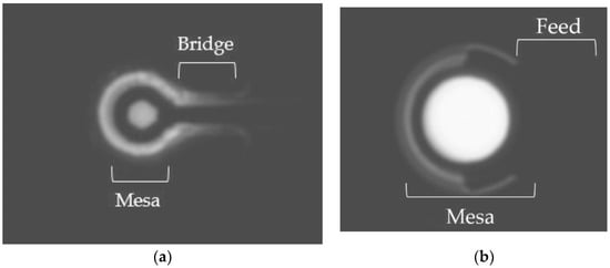
Figure 3.
Near-field images of (a) pumped QF VCSEL, showing light emission along the bridge due to leakage current; (b) pumped standard VCSEL, for comparison.
The increase in threshold current for the 4 μm aperture QF device in comparison to the 6 μm aperture QF device is due in part to the loss mechanisms previously described, however, there is also a proportionally greater leakage current along the bridge due to the high series resistance of the VCSEL in comparison to the larger aperture devices. This explains why the size of the increase with respect to the 6 μm aperture threshold current minimum is greater for the QF devices (0.5 mA) than for the standard VCSELs (0.2 mA), the magnitude of which lies outside the margin of uncertainty determined by the threshold current value calculations.
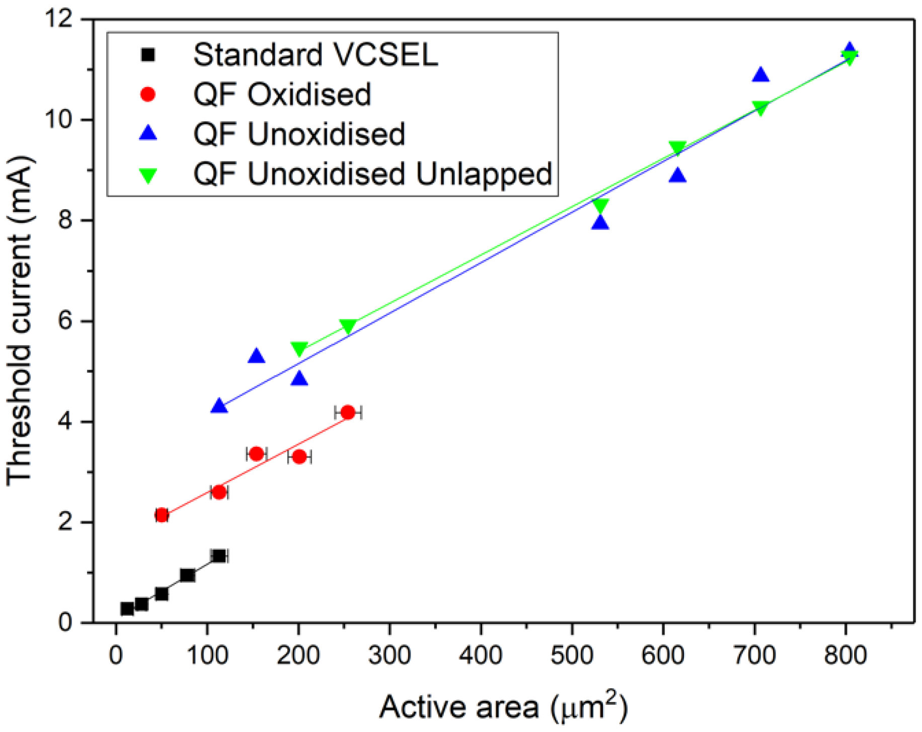
An estimate of the leakage current associated with the bridge-mesa design was made by evaluating the offset in the linear plots of threshold current versus active area, defined here as the area of the oxide aperture. These plots are shown in Figure 4. We exclude outlying high threshold current devices for the evaluation of the leakage offset. By comparing intercepts of the fits, we find a 1.5 0.02 mA offset, which gives the lower limit to the bridge leakage current. There is also an enhancement of surface recombination given that the QF VCSEL mesa sidewalls are exposed relative to the BCB-passivated standard VCSEL mesas, however, this can be treated as another contribution to the leakage current. The leakage current value is calculated from a difference in threshold current, hence the quoted uncertainty is determined by the error in both in threshold current values.
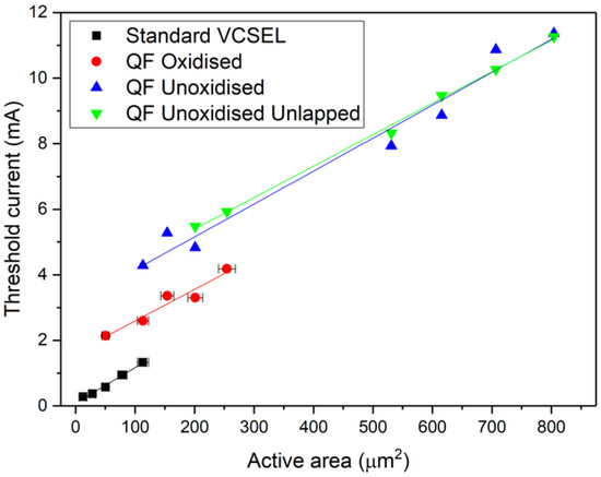
Figure 4.
Lowest measured threshold currents as a function of active area.
We also considered the relative change in performance for QF bridge-mesa devices without an oxide aperture, resulting in a 54% reduction in fabrication time relative to the standard VCSELs. For these devices, there is no insulating oxide layer to channel the injected current and, as such, the leakage current is greater than that of oxidised QF devices. Threshold currents range from 4.3 mA for a 12 μm mesa device, to 11.4 mA for a 32 μm mesa. By, again, comparing the offset in intercepts of the linear plots of threshold current as a function of active area in Figure 4, we find the increase in leakage current to be a further 1.9 0.02 mA relative to an oxidised QF device, where here the active area for unoxidised QF devices is defined as the cross-sectional area of the mesa. Relative to the oxide aperture diameter, the uncertainty in the mesa diameter of the unoxidised devices is negligible, hence we omitted error bars in the plot for these devices.
Finally, we also considered the impact of substrate lapping on the performance of the unoxidised bridge-mesa structures, with the processing time for these devices being reduced by 63% compared to the standard VCSELs. Applying the same treatment as above, we find that lapping does not have a significant impact on threshold current. Values are seen to range from 5.5 mA, for a 12 μm mesa, up to 11.3 mA for a 32 μm mesa, which very closely matches the values for the lapped structures. Additionally, in Figure 4, the dependence on active area is seen to be equivalent to the other structures and there is no offset in intercept relative to the lapped material. This is expected given that the bridge leakage current is independent of the substrate thickness.
Hence, we find that the threshold current of the QF devices is degraded relative to standard structures and, as such, the applicability of this performance characteristic to the application of QF VCSELs for epi-material characterisation in a manufacturing setting is limited by the assumption of a linear offset in threshold behaviour. For greater confidence in the use of QF VCSELs to predict the performance of standard VCSELs, this observed degradation in threshold behaviour should be minimised, however, we are still able to assess device yield and material uniformity with the current form of the QF structures, which will be valuable in manufacturing.
3.2. Output Power
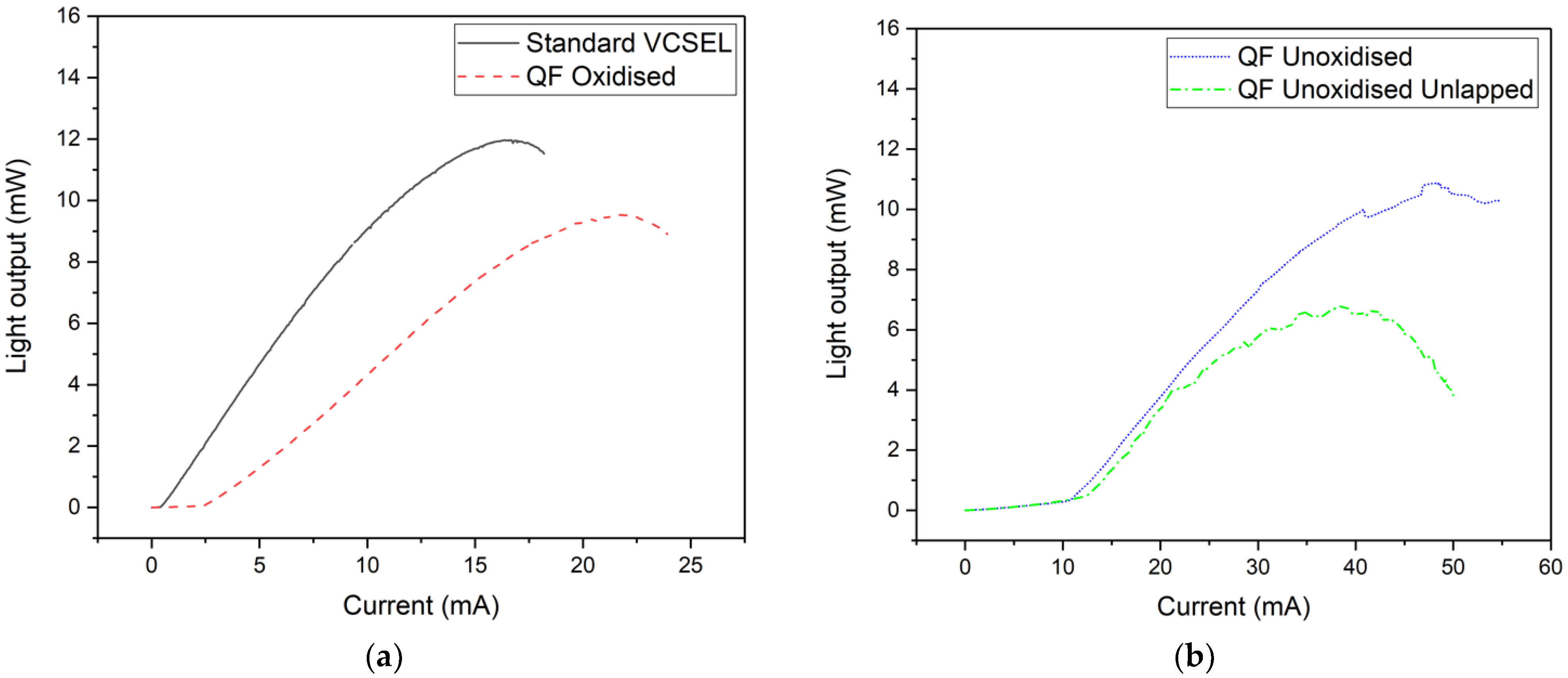
Another important characteristic of VCSEL performance is the emitted optical power. In Figure 5a we compare the light-current characteristics of 6 μm aperture standard and QF devices. The standard VCSEL has a slope efficiency of 0.89 0.04 W/A and produces a peak output power of 12.0 0.36 mW, which is ~3 mW greater than that of the oxidised QF VCSEL, which has a slope efficiency of 0.60 0.03 W/A. The uncertainty in the power measurement is taken from the 3% uncertainty of the integrating sphere at this wavelength range and this, with the resolution of the current source, combines to give the uncertainty in the extracted slope efficiency. We observe the current at which the light output peaks to be greater for the QF VCSEL and we find this to be generally true for the QF devices. This is likely due to the leakage current of the QF VCSELs which, even when comparing equivalent active areas, results in a larger pumped area relative to the standard devices and hence results in a higher current at thermal rollover.
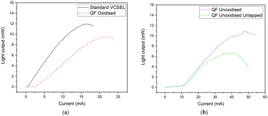
Figure 5.
Light–current characteristics for (a) 6 μm aperture standard and QF VCSEL; (b) 30 μm mesa lapped and unlapped unoxidised QF VCSEL.
In Figure 5b we compare the light-current characteristics of 30 μm mesa lapped and unlapped unoxidised QF VCSELs. The slope efficiency for the unoxidised devices are similar with values of 0.37 and 0.39 0.02 W/A for the lapped and unlapped device, respectively. However, we see that the peak output power is greatest for the lapped device at 11.0 0.33 mW and this is ~4 mW higher than that of the unlapped device. Additionally, the current at which thermal rollover occurs is higher for the lapped device and given that the bridge leakage current of these device is equivalent, we find that the improved heat-sinking properties facilitates higher power output. Additionally, we observe features of instability in the L-I characteristics, occurring around thermal rollover for the lapped device but at much lower currents for the unlapped device. This is likely due to heating-induced mode instability, which we refer to in more detail in the later section on wavelength current tuning.
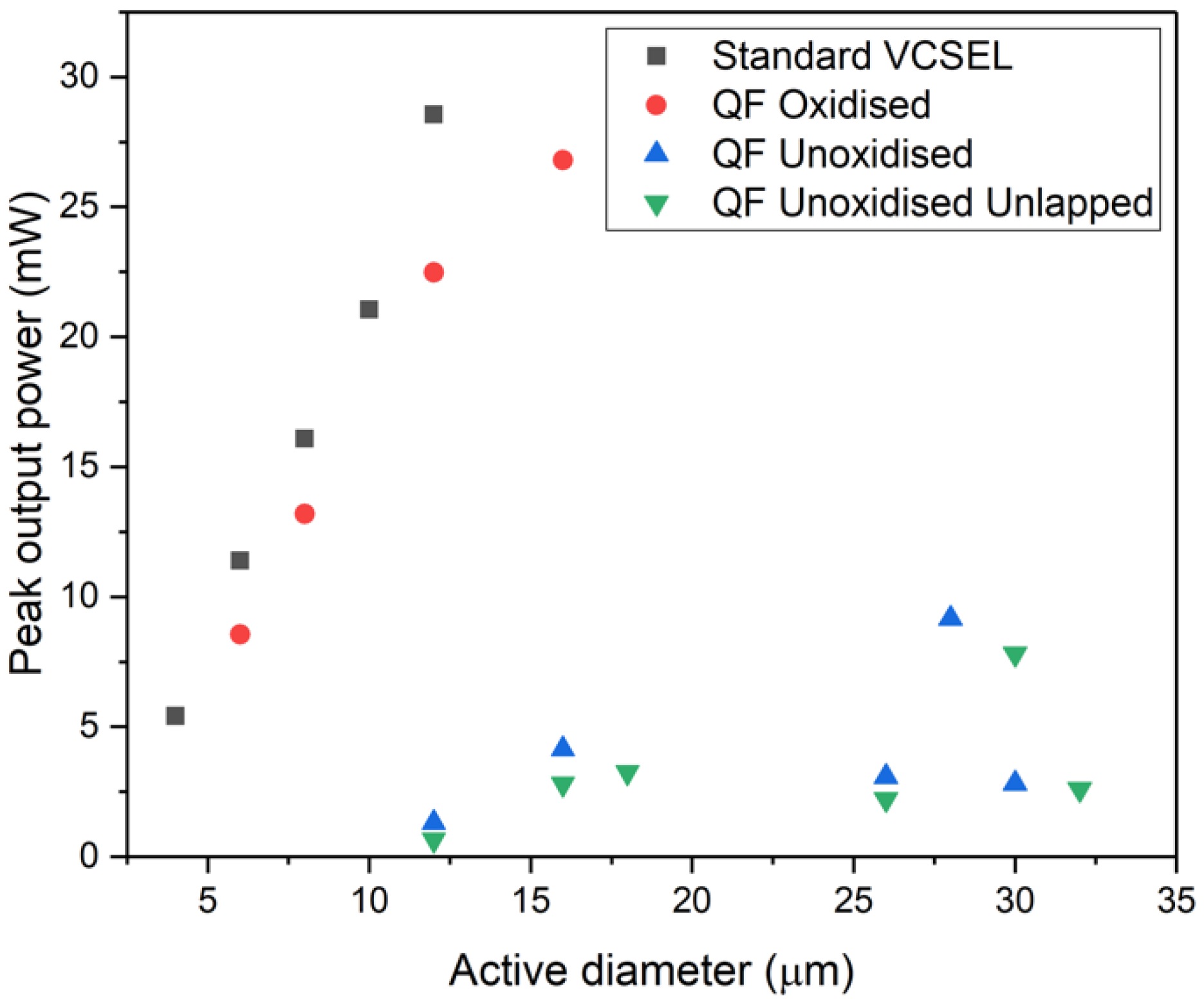
Further, in Figure 6, we compare the mean peak output power as a function of device size for each of the device types. We see a separation between the oxidised and unoxidised devices, with the oxidised devices producing much higher output powers.

Figure 6.
Comparison of peak output power as a function of device size.
In general, the power output of the unoxidised devices is low (<10 mW) and, in comparison to the clear increase with aperture size for the oxidised devices, this remains approximately constant for the full range of device sizes. This may be due to high threshold currents of the unoxidised devices driving internal heating, thus limiting the power output and greater non-radiative recombination at exposed sidewalls.
Although we find that the output characteristics of the QF devices suffer with the rapid fabrication process relative to the standard VCSELs, we still obtain moderate optical powers that would be sufficient for the use of these devices in manufacturing. The mechanisms that result in the observed difference in performance between the QF and standard devices are not immediately observable, hence the predictability of standard device performance from measurements of these QF structures alone is difficult. However, analysis of changes in relative performance across a single wafer, or between wafers with modified epitaxial structures, would still provide valuable information for the purpose of material characterisation in manufacturing.
3.3. Emission Spectra
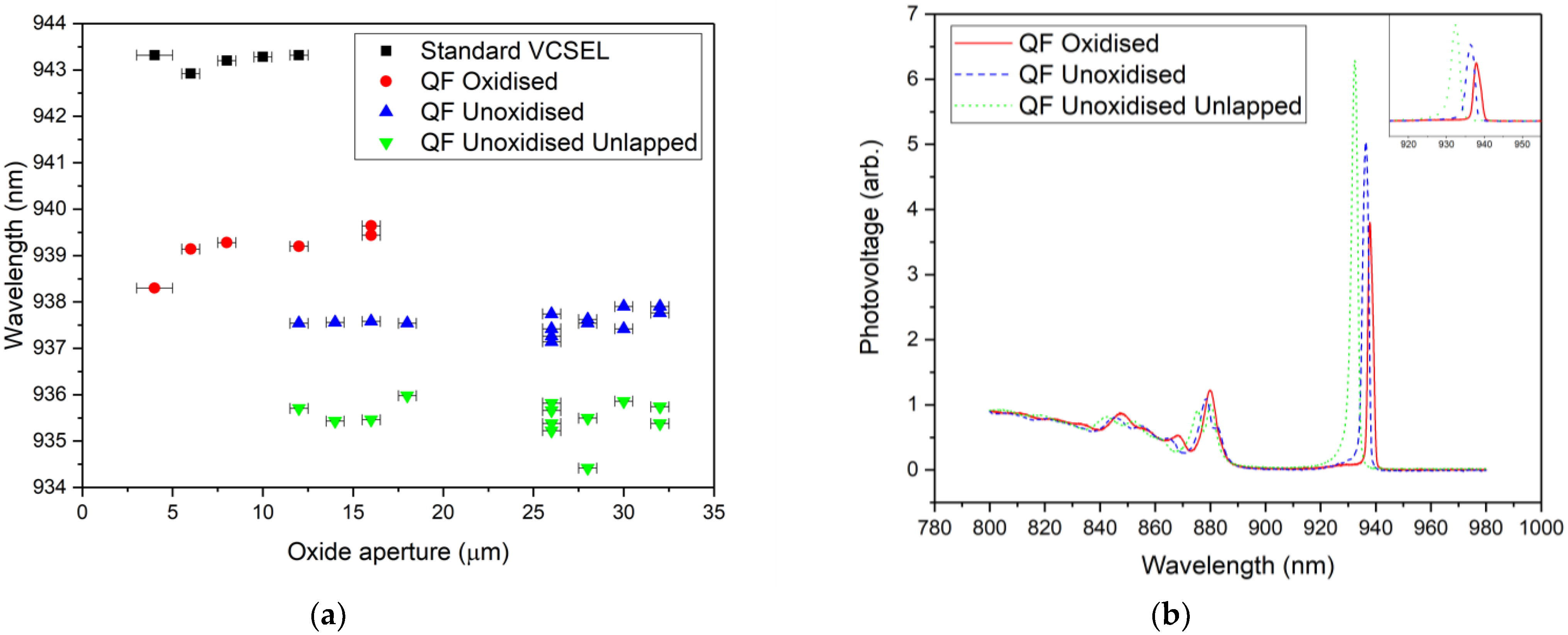
The fundamental mode wavelength for a range of device sizes was extracted from spectral measurements and the resulting plots are shown in Figure 7a. We see that for both the standard VCSELs and QF devices the wavelength remains approximately constant with varying active diameter. We find the mean wavelengths of the standard VCSELs to be 943.2 0.2 nm, and 939.2 0.5 nm for the oxidised QF VCSELs. The error quoted here is given by the standard deviation of the measured wavelengths, quantifying the variation for the different devices driven by spatial variation of the epitaxial material. The mean values differ by ~4 nm and this difference is approximately 6 and 10 nm for the unoxidised and unlapped QF VCSELs, respectively. This is much greater than the measured spread, hence we are confident that this variation across the different device types is driven by spatial variation of the cavity resonance wavelength over the wafer, as opposed to the different fabrication processes. This is also evident in the photovoltage spectra shown in Figure 7b, where the measured material resonance wavelength trends as the measured emission wavelength.
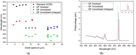
Figure 7.
(a) Lasing wavelengths for all devices; (b) photovoltage spectra for QF VCSEL samples showing the variation in cavity resonance wavelength.
Comparing the mean emission wavelength at threshold of the QF devices to the room temperature cavity resonance wavelength from SPVS measurements, we observe a redshift of 1.4 and 1.2 0.2 nm for the oxidised and unoxidised QF devices, respectively, however, the threshold emission wavelength of the unlapped QF devices is redshifted by 3.1 0.2 nm relative to the cavity resonance. Here, the uncertainty results from the combination of resolutions of the optical spectrum analyser for the wavelength measurement and of the monochromator in the PVS setup. We attribute the observed difference in magnitude of redshift to be a result of self-heating due a combination of high threshold currents and larger thermal resistances associated with the unlapped substrate. Therefore, although the bridge-mesa design incurs a higher threshold current due to the leakage path, this does not translate into a large internal temperature increase for the lapped devices and the impact on the emission wavelength is minimal, however, the effects of greater self-heating are evident in the performance of unlapped devices.
3.4. Wavelength Tuning
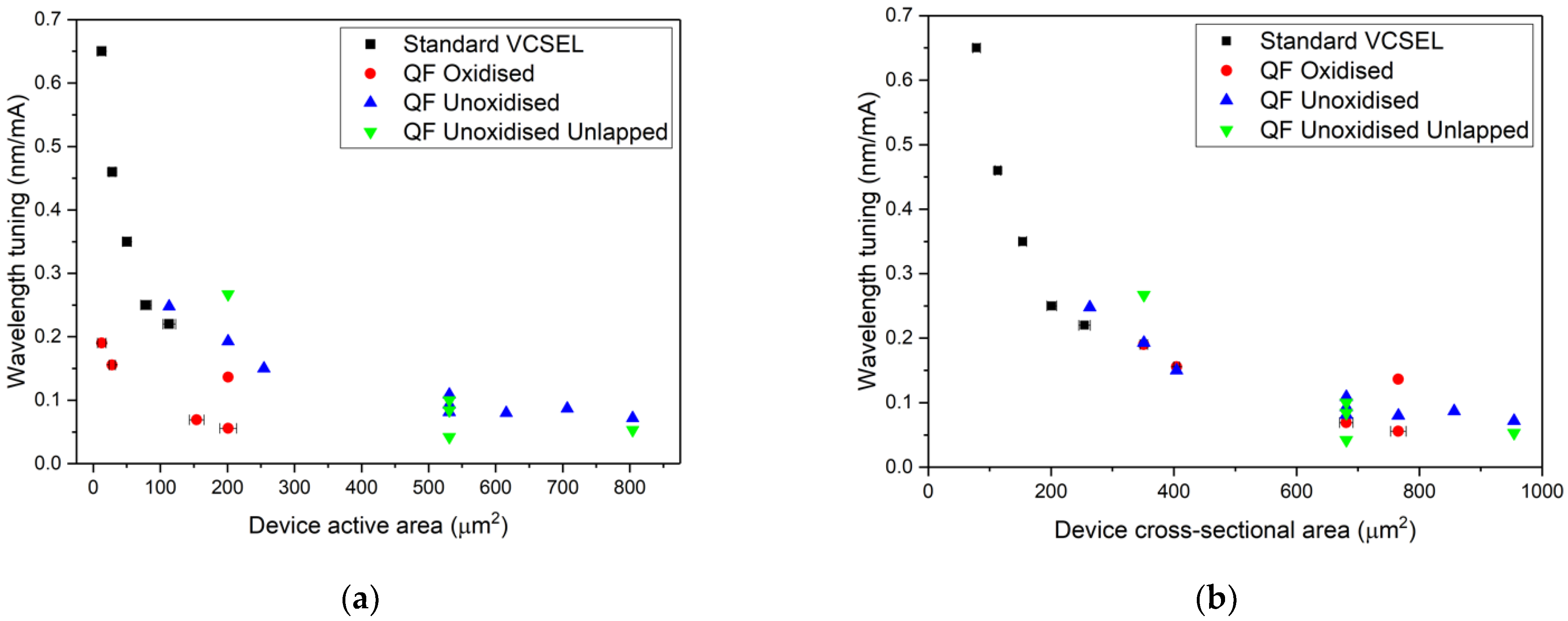
We measured the wavelength shift as a function of temperature for standard VCSEL devices to be 0.07 0.02 nm/K which is in good agreement with the temperature-induced refractive index shift of the epitaxial material [29] and this is expected for all device types given that the constituent materials of the epi-structures are the same. The uncertainty here represents the standard deviation as the spread in measured values. Further, we measured the tuning of the fundamental mode wavelength with increasing injection current and a plot comparing these values for each device type is shown in Figure 8a. Comparing a 4 μm aperture standard VCSEL with a 4 μm aperture QF device we find the redshift in wavelength is 0.65 0.02 and 0.22 0.05 nm/mA, respectively. Using the measured wavelength shift with temperature, these values can be converted to a temperature shift per unit current of 9.3 0.5 K/mA for the standard VCSEL and 2.7 0.7 K/mA for the QF VCSEL. Thus, we find that the standard VCSEL types suffer from greater self-heating which is driven by a combination of an increased electrical and thermal resistance. This uncertainty here derives from the combination of the resolution of the spectrum analyser and that of the current source. In addition, the spread of the measured values of the wavelength shift with temperature combines with that of the wavelength tuning with current to give the uncertainty in the values of temperature shift per unit current.
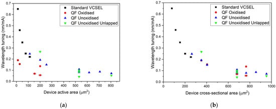
Figure 8.
Tuning of the fundamental mode wavelength with injection current as a function of (a) device active area; (b) total device cross-sectional area, including the oxidised and bridge regions for the QF VCSELs.
The series resistance of the QF VCSELs is reduced compared to the standard VCSELs due to the leakage path along the bridge, which reduces the degree of Joule heating. Additionally, the thermal resistance of the QF VCSELs is reduced due to the significant difference in cross-sectional areas of the devices. This latter point can be seen in Figure 8b where the wavelength tuning with current is plotted as a function of total device cross-sectional area, including the oxidised regions and the bridge regions. The degree of tuning is seen to be proportional to the inverse of the total cross-sectional area, with a much better fit than when only considering the aperture regions of the QF devices. Furthermore, there is an additional contribution to the reduced thermal resistance from the substrate lapping. For the unoxidised QF devices, the wavelength tuning with current for a 12 μm mesa is 0.22 0.04 nm/mA, and the temperature shift with current is then calculated as 3.5 0.7 K/mA—which is similar to the temperature shift of a 4 μm oxide-aperture QF device and within the margin of uncertainty. Although the Joule heating is much greater for the oxidised devices due to the large electrical resistance, the total device cross-sectional area is much greater and hence the thermal resistance is comparatively smaller.
This allows heat to flow away from the active region more easily and facilitates a reduced relative temperature increase for the oxidised device, despite the much smaller active area. Additionally, comparing the wavelength tuning of a 16 μm unlapped unoxidised QF VCSEL to a 4 μm aperture standard device (equivalent mesa diameters), we find the redshift of the emission wavelength to be approximately twice as large for the standard VCSEL. Given that the two devices are of equivalent thermal mass, this difference is attributed to the reduced series resistance, and thus Joule heating, in the QF devices.
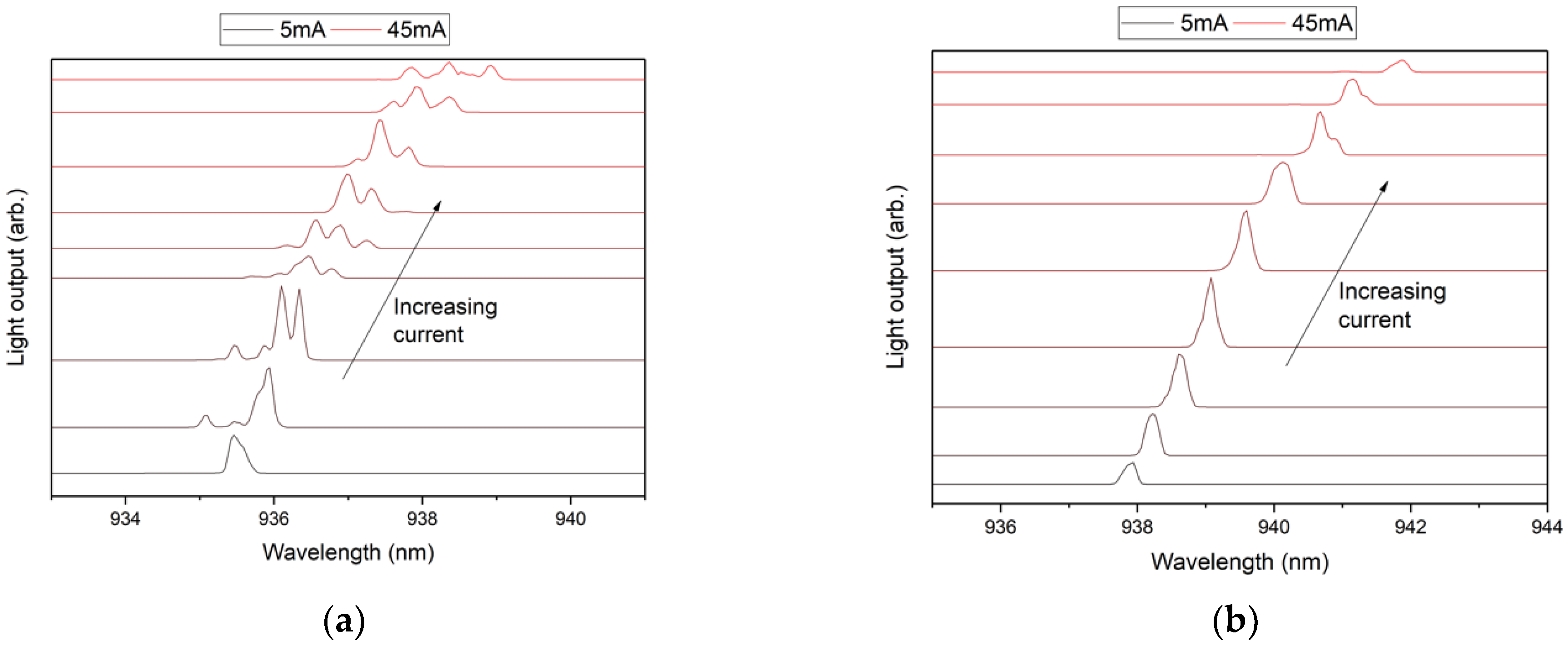
We also compare the wavelength tuning with current for both the lapped and unlapped QF devices. The tuning ranges from 0.05 0.01 nm/mA for a 32 μm mesa device, up to 0.27 0.05 nm/mA for a 16 μm mesa, seen in Figure 8a. This measured wavelength shift is greater than that of a 16 μm mesa lapped device and, given the high threshold currents of the unoxidised QF VCSELs, contributes to the increased redshift of the emission wavelengths at threshold of the unlapped devices. We find that the temperature increase per unit current for a 16 μm mesa diameter (smallest measured unlapped device) is 3.9 0.8 K/mA, which is approximately 1 K/ma higher than that of a 16 μm mesa lapped device, with a temperature shift of 0.19 0.01 K/mA. Hence, we see that lapping has a significant effect on the internal heating of the VCSELs, however, from Figure 8b it is clear that this becomes less significant as the mesa diameter is increased. The variation in uncertainty for the calculated wavelength tuning and temperature shifts is a result of the variation in current ranges used in each measurement, which was dependent on device size and threshold current. Additionally, we observe a difference in the spectral shape between the lapped and unlapped VCSELs. As the CW injection current is increased, we see transverse mode-hopping in the unlapped devices, as shown in the spectra for a 26 μm diameter mesa in Figure 9a. In contrast to this, in Figure 9b, we find that the dominant mode for lapped devices is stable as the injection current is increased, although, at high current some mode-hopping is seen, but this occurs less frequently than for the unlapped devices.
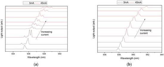
Figure 9.
Emission spectra taken at 5 mA intervals above threshold current for (a) a 26 μm diameter unoxidised unlapped QF VCSEL and (b) a 26 μm diameter unoxidised lapped QF VCSEL, showing mode-hopping in the unlapped device as injection current is increased.
We find this mode-hopping effect to be heating-related by measuring the spectrum of the lapped and unlapped VCSELs above threshold with a pulsed current source. As the pulse length is increased from 5 to 100 μs, with a fixed pulse delay of 200 ns, new peaks in the spectra are observed, corresponding to different transverse modes and the dominant peak is seen to change through the pulse length sweep. Conversely, the dominant mode of the unlapped VCSEL remains constant as the pulse length is increased.
With the analysis of the wavelength tuning of the different device types we observed a favourable thermal resistance for the QF VCSELs, due to reduced electrical and thermal resistance, which has implications for spectral performance at high current. However, we do find that a lack of substrate lapping appreciably degrades the emission spectra at high current.
4. Conclusions
The performance of VCSELs with a simplified fabrication process based on a trench-etch bridge-mesa design was evaluated and compared with that of standard VCSELs based on BCB-planarised isolated mesas. We found that the Quick Fabrication bridge-mesa VCSELs gave emission wavelength data that was representative of the epitaxial material, as shown by photovoltage spectroscopy measurements. The bridge-mesa VCSELs incurred a relative increase in threshold current of 1.5 0.1 and 3.4 0.1 mA for the oxidised and unoxidised structures, respectively. This increase in threshold current was principally driven by the parallel leakage path associated with the bridge design, but also includes the effect of increased surface recombination due to the unpassivated mesa sidewalls. Additionally, the QF VCSELs suffered with reduced slope efficiencies relative to standard devices and, despite the onset of thermal rollover occurring at higher injection currents, the peak output powers were also less than that of the standard VCSELs. We found the effect of substrate lapping to be significant for high current performance, with a high degree of mode hopping seen for unlapped QF VCSELs, a comparatively large wavelength redshift with increasing bias, reduced peak output powers and thermal rollover consistently occurring at lower currents above threshold.
In summary, we find that these Quick Fabrication VCSELs can provide some valuable information about the constituent epitaxial material and in a time reduced by up to 63% relative to the standard VCSELs, and, in this respect, this fabrication method can be implemented in a commercial setting with minimal impact. As variations due to the fabrication are no more prominent than for standard VCSEL devices, analysis of relative changes in performance of the QF VCSELs across a wafer would still be useful for the assessment of device yield and material uniformity on a given wafer, and to assess reactor drift across a growth campaign. However, the employment of a bridge-mesa design results in a reduction in electro-optic performance, primarily an increase in threshold current and reduced efficiency, and, although the impact on the spectral properties is minimal, we conclude that these QF structures can only be applied to the prediction of standard device performance in a limited way. For full application of this method, the degradation of the QF VCSEL performance relative to standard devices, principally driven by the leakage current, should be mitigated. However, in this study the fundamental knowledge required for implementing these methods of producing stripped-back devices capable of predicting performance of typical structures was laid out. Finally, though this work was performed on epitaxial material designed for 940 nm emission, the fabrication method employed is not limited to the epi-structure used and therefore can be adopted for other VCSEL structures (using equivalent p-i-n layout), for various applications and emission wavelengths.
Author Contributions
Conceptualisation, S.S. and P.M.S.; methodology, J.B., C.P.A., S.-J.G. and S.S.; validation, J.B., C.P.A., D.G.H., C.H., S.-J.G., S.S. and P.M.S.; formal analysis, J.B.; investigation, J.B, R.F., J.N., D.G.H., S.-J.G. and C.H.; resources, J.I.D.; data curation, J.B., R.F, J.N., C.H. and C.P.A.; writing—original draft preparation, J.B.; writing—review and editing, J.B., C.P.A., S.-J.G., S.S. and P.M.S.; visualisation, J.B., C.P.A. and S.S.; supervision, S.S. and P.M.S.; project administration, S.S. and P.M.S.; funding acquisition, S.S. and P.M.S. All authors have read and agreed to the published version of the manuscript.
Funding
This research forms part of the Future Compound Semiconductor Manufacturing Hub, funded by the Engineering and Physical Sciences Research Council (EPSRC), grant number EP/P006973/1. The APC was provided by a UKRI research fund. Funding was also provided in the form of an EPSRC-funded iCASE PhD studentship, co-sponsored by IQE plc., grant number EP/T517525/1.
Institutional Review Board Statement
Not applicable.
Informed Consent Statement
Not applicable.
Data Availability Statement
Due to confidentiality agreements with research collaborators, supporting data can only be made available to bona fide researchers subject to a non-disclosure agreement. Details of the data and how to request access are available at the Cardiff University Research Data Archive at http://doi.org/10.17035/d.2021.0140858939.
Acknowledgments
The authors would like to acknowledge support from IQE plc in the supply of epitaxial material and technical support from the Institute for Compound Semiconductors at Cardiff University for device fabrication.
Conflicts of Interest
The authors declare no conflict of interest. The funders had no role in the design of the study; in the collection, analyses, or interpretation of data; in the writing of the manuscript, or in the decision to publish the results.
References
- Iga, K. Vertical-Cavity Surface-Emitting Laser: Its Conception and Evolution. Jpn. J. Appl. Phys. 2008, 47, 1–10. [Google Scholar] [CrossRef]
- Koyama, F. Recent Advances of VCSEL Photonics. J. Light. Technol. 2006, 24, 4502–4513. [Google Scholar] [CrossRef]
- Liu, A.; Wolf, P.; Lott, J.A.; Bimberg, D. Vertical-cavity surface-emitting lasers for data communication and sensing. Photonics Res. 2019, 7, 121–136. [Google Scholar] [CrossRef]
- Khan, Z.; Shih, J.-C.; Chao, R.-L.; Tsai, T.-L.; Wang, H.-C.; Fan, G.-W.; Lin, Y.-C.; Shi, J.-W. High-brightness and high-speed vertical-cavity surface-emitting laser arrays. Optica 2020, 7, 267. [Google Scholar] [CrossRef]
- Hayes, D.G.; Peach, T.; Baker, J.; Gillgrass, S.J.; Allford, C.P.; Sobiesierski, A.; Eng, C.; Shabbir, S.; Thomas, S.; Hentschel, C.; et al. 150 mm full wafer fabrication and characterization of 940nm emitting VCSELs for high-volume manufacture. In Vertical-Cavity Surface-Emitting Lasers XXV; Society of Photo-Optical Instrumentation Engineers (SPIE): San Francisco, CA, USA, 2021; Volume 11704, p. 1170406. [Google Scholar] [CrossRef]
- Johnson, A.; Joel, A.; Clark, A.; Pearce, D.; Geen, M.; Wang, W.; Pelzel, R.; Lim, S.W. High performance 940nm VCSELs on large area germanium substrates: The ideal substrate for volume manufacture. In Vertical-Cavity Surface-Emitting Lasers XXV; Society of Photo-Optical Instrumentation Engineers (SPIE): San Francisco, CA, USA, 2021; Volume 11704, p. 1. [Google Scholar] [CrossRef]
- Bowen, D.K.; Wormington, M.; Feichtinger, P.; Joyce, D.E. Full-Wafer Defect Identification using X-ray Topography. AIP Conf. Proc. 2003, 683, 284–288. [Google Scholar] [CrossRef]
- Hou, H.; Chui, H.; Choquette, K.; Hammons, B.; Breiland, W.; Geib, K. Highly uniform and reproducible vertical-cavity surface-emitting lasers grown by metalorganic vapor phase epitaxy with in situ reflectometry. IEEE Photonics Technol. Lett. 1996, 8, 1285–1287. [Google Scholar] [CrossRef]
- Lei, C.; Deng, H.; Dudley, J.; Lim, S.; Liang, B.; Tashima, M.; Herrick, R. Manufacturing of oxide VCSEL at Hewlett Packard. In 1999 Digest of the LEOS Summer Topical Meetings: Nanostructures and Quantum Dots/WDM Components/VCSELs and Microcavaties/RF Photonics for CATV and HFC Systems (Cat. No. 99TH8455); IEEE: San Diego, CA, USA, 1999; pp. 11–12. [Google Scholar] [CrossRef]
- Kim, Y.K.; Choquette, K.D.; Baker, J.E.; Allerman, A.A. Secondary ion mass spectrometry analysis of vertical cavity surface-emitting lasers. J. Vac. Sci. Technol. B Microelectron. Nanometer Struct. 2004, 22, 949. [Google Scholar] [CrossRef]
- Singh, J.; Bajaj, K.K.; Chaudhuri, S. Theory of photoluminescence line shape due to interfacial quality in quantum well structures. Appl. Phys. Lett. 1984, 44, 805–807. [Google Scholar] [CrossRef]
- Huffaker, D.L.; Deppe, D.G.; Kumar, K.; Rogers, T.J. Native-oxide defined ring contact for low threshold vertical-cavity lasers. Appl. Phys. Lett. 1994, 65, 97–99. [Google Scholar] [CrossRef]
- Lear, K.; Choquette, K.; Schneider, R.; Kilcoyne, S.; Geib, K. Selectively oxidised vertical cavity surface emitting lasers with 50% power conversion efficiency. Electron. Lett. 1995, 31, 208–209. [Google Scholar] [CrossRef]
- MacDougal, M.; Dapkus, P.; Pudikov, V.; Zhao, H.; Yang, G.M. Ultralow threshold current vertical-cavity surface-emitting lasers with AlAs oxide-GaAs distributed Bragg reflectors. IEEE Photonics Technol. Lett. 1995, 7, 229–231. [Google Scholar] [CrossRef]
- Geels, R.; Corzine, S.; Scott, J.; Young, D.; Coldren, L. Low threshold planarized vertical-cavity surface-emitting lasers. IEEE Photonics Technol. Lett. 1990, 2, 234–236. [Google Scholar] [CrossRef]
- Chua, C.; Thornton, R.; Treat, D. Planar laterally oxidized vertical-cavity lasers for low-threshold high-density top-surface-emitting arrays. IEEE Photon- Technol. Lett. 1997, 9, 1060–1062. [Google Scholar] [CrossRef]
- Coldren, L.A.; Corzine, S.W.; Mashanovitch, M. Diode Lasers and Photonic Integrated Circuits; Wiley: Hoboken, NJ, USA, 2012. [Google Scholar]
- Grabherr, M.; Jager, R.; Miller, M.; Thalmaier, C.; Herlein, J.; Michalzik, R.; Ebeling, K. Bottom-emitting VCSEL’s for high-CW optical output power. IEEE Photonics Technol. Lett. 1998, 10, 1061–1063. [Google Scholar] [CrossRef]
- Khan, Z.; Shih, J.-C.; Cheng, C.-L.; Shi, J.-W. High-Power and Highly Single-Mode Zn-Diffusion VCSELs at 940 nm Wavelength. In 2019 IEEE Photonics Conference (IPC); IEEE: San Antonio, CA, USA, 2019. [Google Scholar] [CrossRef]
- Khan, Z.; Ledentsov, N.; Chorchos, L.; Shih, J.-C.; Chang, Y.-H.; Shi, J.-W. Single-Mode 940 nm VCSELs With Narrow Divergence Angles and High-Power Performances for Fiber and Free-Space Optical Communications. IEEE Access 2020, 8, 72095–72101. [Google Scholar] [CrossRef]
- Chaqmaqchee, F.; Lott, J. Impact of oxide aperture diameter on optical output power, spectral emission, and bandwidth for 980 nm VCSELs. OSA Contin. 2020, 3, 2602–2613. [Google Scholar] [CrossRef]
- Das, N.C.; Chang, W. Mesa-size dependence characteristics of vertical surface-emitting lasers. J. Electron. Mater. 2004, 33, 972–976. [Google Scholar] [CrossRef]
- Wipiejewski, T.; Peters, M.; Thibeault, B.; Young, D.; Coldren, L. Size-dependent output power saturation of vertical-cavity surface-emitting laser diodes. IEEE Photonics Technol. Lett. 1996, 8, 10–12. [Google Scholar] [CrossRef]
- Baveja, P.P.; Kögel, B.; Westbergh, P.; Gustavsson, J.S.; Haglund, Å.; Maywar, D.; Agrawal, G.; Larsson, A. Assessment of VCSEL thermal rollover mechanisms from measurements and empirical modeling. Opt. Express 2011, 19, 15490–15505. [Google Scholar] [CrossRef]
- Sale, T.E. Vertical Cavity Surface Emitting Lasers. Ph.D. Thesis, University of Sheffield, Sheffield, UK, 1993. [Google Scholar]
- Michalzik, R. VCSELs: Fundamentals, Technology and Applications of Vertical-Cavity Surface Emitting Lasers; Springer: Berlin/Heidelberg, Germany, 2012. [Google Scholar]
- Koyama, F.; Kinoshita, S.; Iga, K. Room-temperature continuous wave lasing characteristics of a GaAs vertical cavity surface-emitting laser. Appl. Phys. Lett. 1989, 55, 221–222. [Google Scholar] [CrossRef]
- Tell, B.; Brown-Goebeler, K.F.; Leibenguth, R.E.; Baez, F.M.; Lee, Y.H. Temperature dependence of GaAs-AlGaAs vertical cavity surface emitting lasers. Appl. Phys. Lett. 1992, 60, 683–685. [Google Scholar] [CrossRef]
- Khan, N.I.; Choudhury, S.H.; Roni, A.A. A comparative study of the temperature dependence of lasing wavelength of conventional edge emitting stripe laser and vertical cavity surface emitting laser. In Proceedings of the International Conference on Optical Communication Systems, Seville, Spain, 18–21 July 2011. [Google Scholar]
- Jung, C.; Jäger, R.; Grabherr, M.; Schnitzer, P.; Michalzik, R.; Weigl, B.; Müller, S.; Ebeling, K. 4.8 mW singlemode oxide confined top-surface emitting vertical-cavity laser diodes. Electron. Lett. 1997, 33, 1790–1791. [Google Scholar] [CrossRef]
- Ashkenasy, N.; Leibovitch, M.; Rosenwaks, Y.; Shapira, Y. Characterization of quantum well structures using surface photovoltage spectroscopy. Mater. Sci. Eng. B 2000, 74, 125–132. [Google Scholar] [CrossRef][Green Version]
- Liang, J.S.; Huang, Y.S.; Tien, C.W.; Chang, Y.M.; Chen, C.W.; Li, N.Y.; Li, P.W.; Pollak, F.H. Surface photovoltage spectroscopy characterization of a GaAs/GaAlAs vertical-cavity-surface-emitting-laser structure: Angle dependence. Appl. Phys. Lett. 2001, 79, 3227–3229. [Google Scholar] [CrossRef][Green Version]
- Huang, Y.S.; Malikova, L.; Pollak, F.H.; Debray, J.-P.; Hoffman, R.; Amtout, A.; Stall, R.A. Surface photovoltage spectroscopy and normal-incidence reflectivity characterization of a 1.3 μm InGaAlAs/InP vertical-cavity surface-emitting laser structure. J. Appl. Phys. 2002, 91, 6203–6205. [Google Scholar] [CrossRef]
- Thibeault, B.J.; Strand, T.A.; Wipiejewski, T.; Peters, M.G.; Young, D.B.; Corzine, S.W.; Coldren, L.A.; Scott, J.W. Evaluating the effects of optical and carrier losses in etched-post vertical cavity lasers. J. Appl. Phys. 1995, 78, 5871–5875. [Google Scholar] [CrossRef]
- Choquette, K.D.; Chow, W.W.; Hadley, G.R.; Hou, H.Q.; Geib, K.M. Scalability of small-aperture selectively oxidized vertical cavity lasers. Appl. Phys. Lett. 1997, 70, 823–825. [Google Scholar] [CrossRef]
- Jungo, M.; Di Sopra, F.M.; Erni, D.; Baechtold, W. Scaling effects on vertical-cavity surface-emitting lasers static and dynamic behavior. J. Appl. Phys. 2002, 91, 5550–5557. [Google Scholar] [CrossRef]
- Young, D.; Scott, J.; Malhotra, V.; Coldren, L.; Kapila, A. Reduced threshold vertical-cavity surface-emitting lasers. Electron. Lett. 1994, 30, 233–235. [Google Scholar] [CrossRef]
- Naidu, D. Characterisation of Lateral Carrier Out-Diffusion and Surface Recombination in Ridge Waveguide Devices-ORCA. Ph.D. Thesis, Cardiff University, Cardiff, UK, 2009. [Google Scholar]
- Sale, T.E.; Roberts, J.S.; David, J.P.R.; Grey, R.; Woodhead, J.; Robson, P.N. Temperature effects in VCSELs. In Vertical-Cavity Surface-Emitting Lasers; Society of Photo-Optical Instrumentation Engineers (SPIE): San Jose, CA, USA, 1997; Volume 3003, pp. 100–110. [Google Scholar] [CrossRef]
- Chen, C.; Leisher, P.; Allerman, A.A.; Geib, K.; Choquette, K. Temperature Analysis of Threshold Current in Infrared Vertical-Cavity Surface-Emitting Lasers. IEEE J. Quantum Electron. 2006, 42, 1078–1083. [Google Scholar] [CrossRef]
Publisher’s Note: MDPI stays neutral with regard to jurisdictional claims in published maps and institutional affiliations. |
© 2021 by the authors. Licensee MDPI, Basel, Switzerland. This article is an open access article distributed under the terms and conditions of the Creative Commons Attribution (CC BY) license (https://creativecommons.org/licenses/by/4.0/).


