Article

The Effect of an Ag Nanofilm on Low-Temperature Cu/Ag-Ag/Cu Chip Bonding in Air

1
Department of Manufacturing Systems and Design Engineering, Seoul National University of Science and Technology, Seoul 01811, Korea
2
Department of Semiconductor Engineering, Seoul National University of Science and Technology, Seoul 01811, Korea
*
Author to whom correspondence should be addressed.
Appl. Sci. 2021, 11(20), 9444; https://doi.org/10.3390/app11209444
Submission received: 7 September 2021 / Revised: 5 October 2021 / Accepted: 8 October 2021 / Published: 12 October 2021

Abstract

:
Low-temperature Cu-Cu bonding technology plays a key role in high-density and high-performance 3D interconnects. Despite the advantages of good electrical and thermal conductivity and the potential for fine pitch patterns, Cu bonding is vulnerable to oxidation and the high temperature of the bonding process. In this study, chip-level Cu bonding using an Ag nanofilm at 150 °C and 180 °C was studied in air, and the effect of the Ag nanofilm was investigated. A 15-nm Ag nanofilm prevented Cu oxidation prior to the Cu bonding process in air. In the bonding process, Cu diffused rapidly to the bonding interface and pure Cu-Cu bonding occurred. However, some Ag was observed at the bonding interface due to the short bonding time of 30 min in the absence of annealing. The shear strength of the Cu/Ag-Ag/Cu bonding interface was measured to be about 23.27 MPa, with some Ag remaining at the interface. This study demonstrated the good bonding quality of Cu bonding using an Ag nanofilm at 150 °C.

1. Introduction

Although semiconductor devices have achieved remarkable performance improvement and miniaturization of integrated circuits according to Moore’s law, semiconductor devices have reached a physical limit in miniaturization, and device scaling means it becomes very difficult to improve the degree of integration due to the rapidly increasing number of inputs/outputs. To improve the degree of integration of semiconductor devices, 3D packaging technologies such as wafer stacking and die stacking are becoming increasingly important, especially in recent heterogeneous integration, and many studies on 3D packaging have been conducted that cover high performance, miniaturization, reliability, and low manufacturing cost [1,2]. Si forming and filling, wafer thinning, and the bonding process are required for 3D packaging fabrication, and the most important unit process is currently the Cu bonding process due to the fine pitch structure and high-performance demands. Although Cu has a relatively low cost, fine pitch pattern-ability, and good electrical and thermal conductivities, Cu suffers from needing a high bonding temperature, which is typically higher than 400 °C, and of forming a natural oxide film even with low oxygen content [3]. If the Cu bonding process takes place at above 400 °C, the device performance can potentially degrade because the device is made of many metal interconnects. In addition, if Cu oxide is formed on the Cu surface before bonding, Cu bonding is not well formed, and electrical failure occurs in the bonded interconnect.
Many low-temperature Cu bonding studies have been actively published [3,4,5,6,7,8,9,10,11,12,13,14]. Tan et al., reported the results of low-temperature Cu bonding at 250 °C after preventing oxidation of the Cu surface using a self-assembled monolayer surface treatment [4], and more recently, the use of a mixed gas plasma of argon (Ar) and nitrogen (N2) [5] prior to Cu bonding has been reported to prevent Cu oxidation. Elsewhere, Kim et al., presented sequential two-step Ar and N2 plasma surface treatments to form uniform copper nitride (Cu4N) as an antioxidant layer on the Cu surface and allow Cu bonding at 260 °C and 300 °C [6,7]. To lower the Cu bonding temperature below 200 °C, the use of various metal passivation layers has been reported. Huang et al., reported oxidation prevention and low-temperature Cu bonding at 180 °C using an ultra-thin Ti layer [8], and Vanjari et al., reported Cu bonding at 160 °C using an ultra-thin Ti layer [9]. Bonan et al., reported low-temperature Cu bonding at 140 °C using an Au passivation layer [10]. Chen et al., presented Cu chip bonding at 180 °C using an Ag thin film deposited by sputtering [11]. In addition, Cu bonding research using Ag nanoparticles has been conducted because of the nanoparticles’ high specific surface area, high diffusion rate, and low deformation. Liu et al., and Hu et al., reported Cu bonding results without voids at the bonding interface at 180 °C using Ag nanoparticles deposited by pulsed laser deposition [12,13].
Cu bonding at 150 °C and 180 °C and solid-state diffusion using an Ag nanofilm without forming an intermetallic compound were studied herein. Ag nanofilm deposited by an evaporation process produces a porous film and has a high surface area, and evaporation is a more CMOS-compatible process than are other nanoparticle or nanotube processes. The solid-state diffusion of the Ag nanofilm was investigated, and low-temperature Cu bonding using an Ag nanofilm was evaluated for 3D system-in-package applications.

2. Materials and Methods

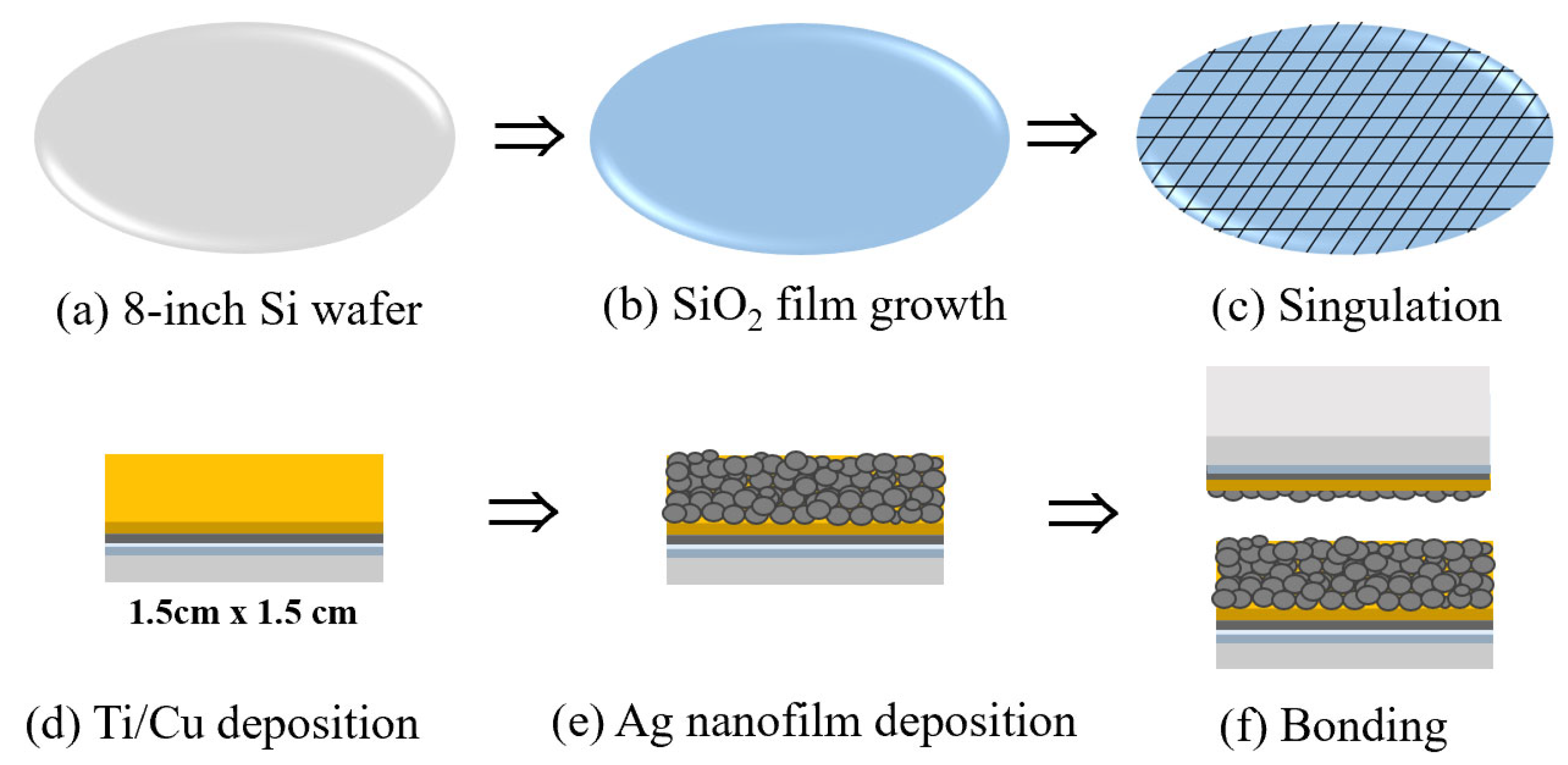
A 700-nm-thick silicon oxide (SiO2) film using an oxidation furnace was grown on an 8 inch silicon wafer (p-type, 100). Then, the Cu wafer was singulated into 1.5 cm (W) × 1.5 cm (L) chips. The 50-nm-thick Ti and 1-μm-thick Cu thin films were sequentially deposited on diced Si wafers by DC sputtering at a power of 2500 W under a pressure of 3.7 × 10⁻³ torr. Thereafter, a porous Ag nanofilm with an average thickness of about 15 nm was deposited over the Cu film using an e-beam evaporator; the deposition rate of Ag was about 1 nm/s. After dissolving about 70% of the Ag in 3–5 nm granules in the e-beam evaporator, Ag nanofilm deposition was undertaken at a working pressure below 2.7 × 10⁻⁶ torr. A low working pressure is required for preventing contaminations and minimizing scattering due to Ag colliding with molecules in the vapor phase. The solid-state diffusion behavior of the Ag nanofilm on Cu was evaluated by heating each sample on a hot plate in air and by analyzing depth profiles using high performance X-ray photoelectron spectroscopy (HPXPS; K-Alpha, Thermo Fisher Scientific, Waltham, MA, USA). HPXPS was pe rformed at KBSI (Korea Basic Science Institute) and the measurement resolution was less than 0.5 eV FWHM (full width at half maximum).
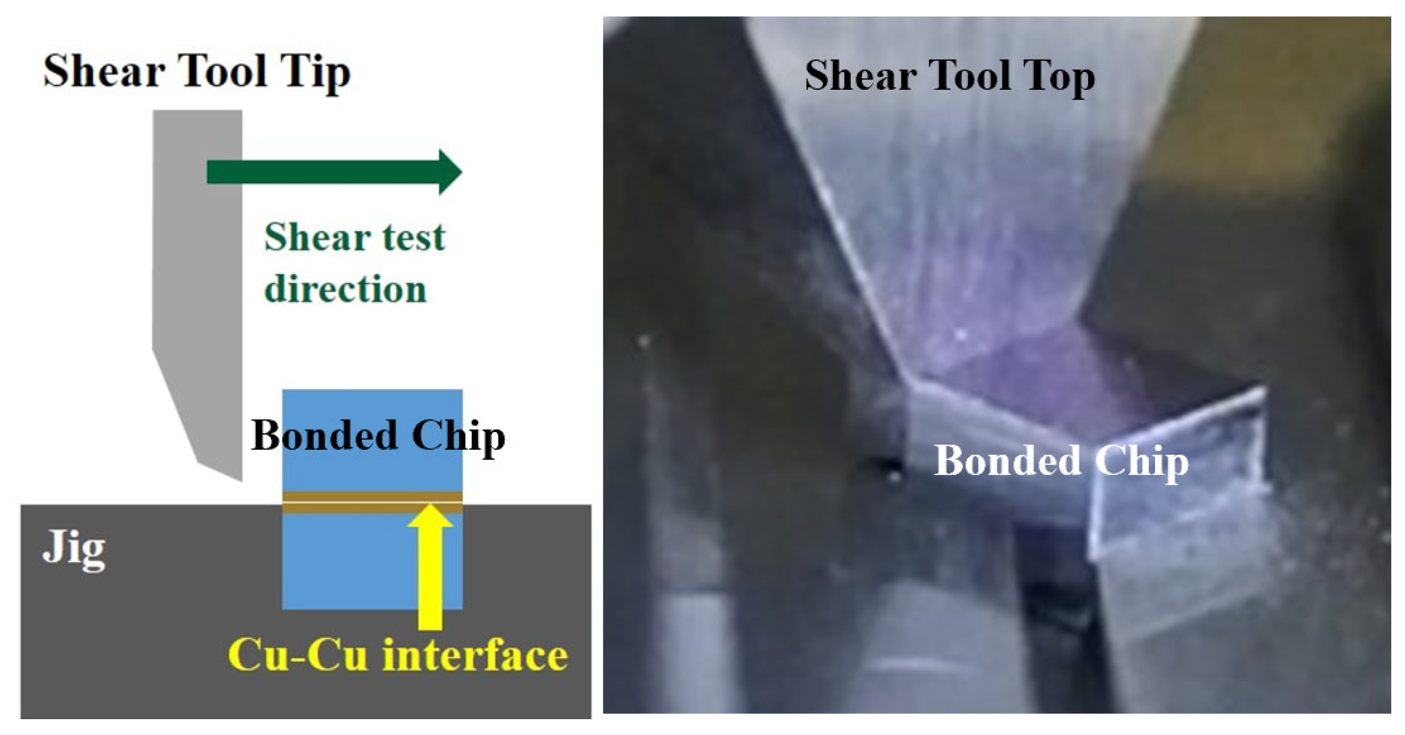
For the Cu bonding using the Ag nanofilm, the top and bottom chips were bonded using a heating press (D3p-05j, Daeheung Science) at 150 °C and 180 °C under 30 MPa pressure for 30 min as shown in Table 1. The sample preparation process is schematically illustrated in Figure 1. The quality of the bonding interface was analyzed by shear measurement (DAGE 4800, DAKO). For the shear measurement, the bonded chips were singulated into 2 × 2 mm size. Photographic images of the shear test are presented in Figure 2. In addition, the bonding interface was evaluated structurally by field-emission scanning electron microscopy (FESEM; Apreo S HiVac, FEI), energy dispersive spectroscopy (EDS; Xflash 6-100, BRUKER), and transmission electron microscopy (TEM; TM 80-300, Titan).

3. Results and Discussion

3.1. Ag Diffusion into Cu

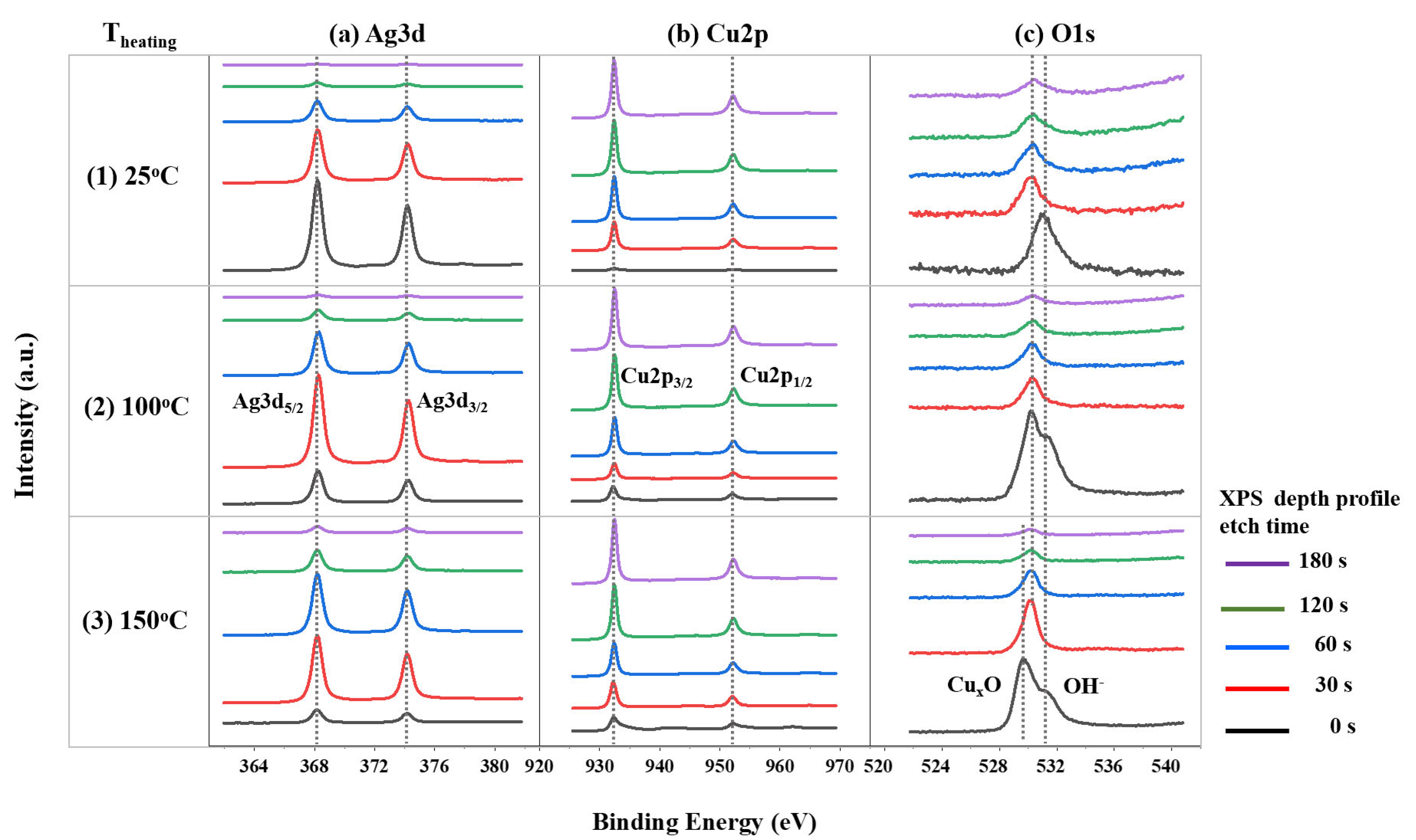
The Ag nanofilm deposited on the Cu(111) was about 15 nm thick, and was deposited as a rather porous film, not in the form of a uniform and dense crystalline thin film [14]. As shown in Figure 3, the Ag3d and Cu2p XPS profiles at the surface (i.e., the profile of XPS etch time at 0 s) show no oxidation of Cu, which indicates that the porous Ag nanofilm was sufficient in preventing oxidation of the Cu surface at room temperature.
The Ag nanofilms on the Cu samples were maintained at RT (25 °C), 100 °C, 150 °C, and 200 °C for one hour on a hot plate to analyze the diffusion behavior of Ag and Cu. Then, XPS depth profiling was performed, and the results are presented in Figure 3. As the temperature increased, the Ag concentration on the surface decreased and the Cu concentration increased. Even in the O1s profile, surface oxidation by the Ag nanofilm hardly occurred at room temperature, but as the temperature increased, Cu diffused to the surface and surface oxidation occurred rapidly. The activation energy of Ag to Cu was about 3.95 times higher than that of Cu to Ag [14]. According to our previous study [14], the activation energy and the pre-exponential factor were 17,876 J/mol and 0.064 m2/s, respectively. Therefore, the diffusion coefficient of Ag to Cu at 180 °C was determined to be 5.56 × 10⁻⁴ m2/s, which is much faster than the diffusion of 200 nm Ag into single crystal Cu or bulk Ag into Cu [15,16]. This is explained by the rapid progress of Cu diffusion into the porous Ag nanofilm. This is in reasonable agreement with Ag diffusion into Cu at high temperature. But, unlike the lattice diffusion between bulk Ag and Cu at high temperature, Ag nanofilm diffusion into Cu occurs mostly through grain boundary diffusion, indicating a high diffusion coefficient and low activation energy [16]. At high temperatures, atomic diffusion occurs generally by substitutional diffusion, but at low temperatures, atomic diffusion occurs mostly by grain boundary diffusion rather than bulk diffusion because the activation energy of grain boundary diffusion is generally half that for bulk diffusion [16,17].

3.2. Cu/Ag-Ag/Cu Bonding

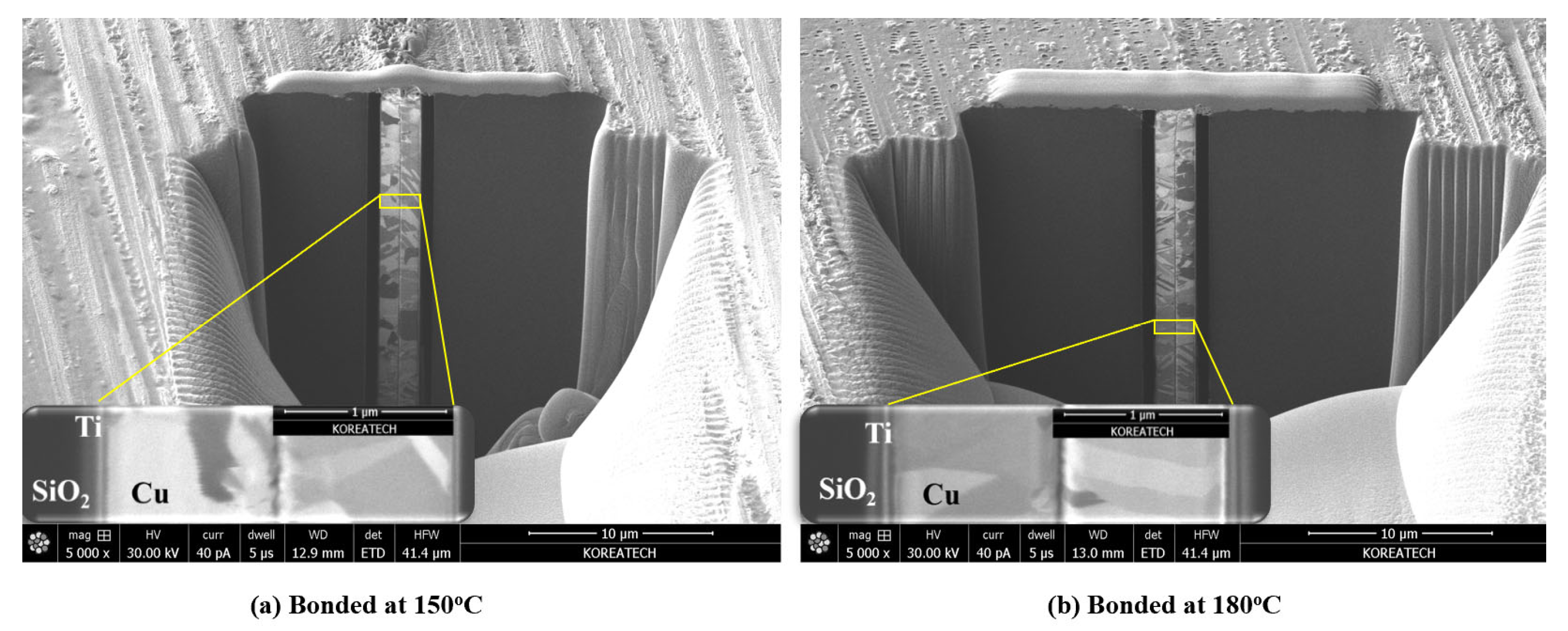
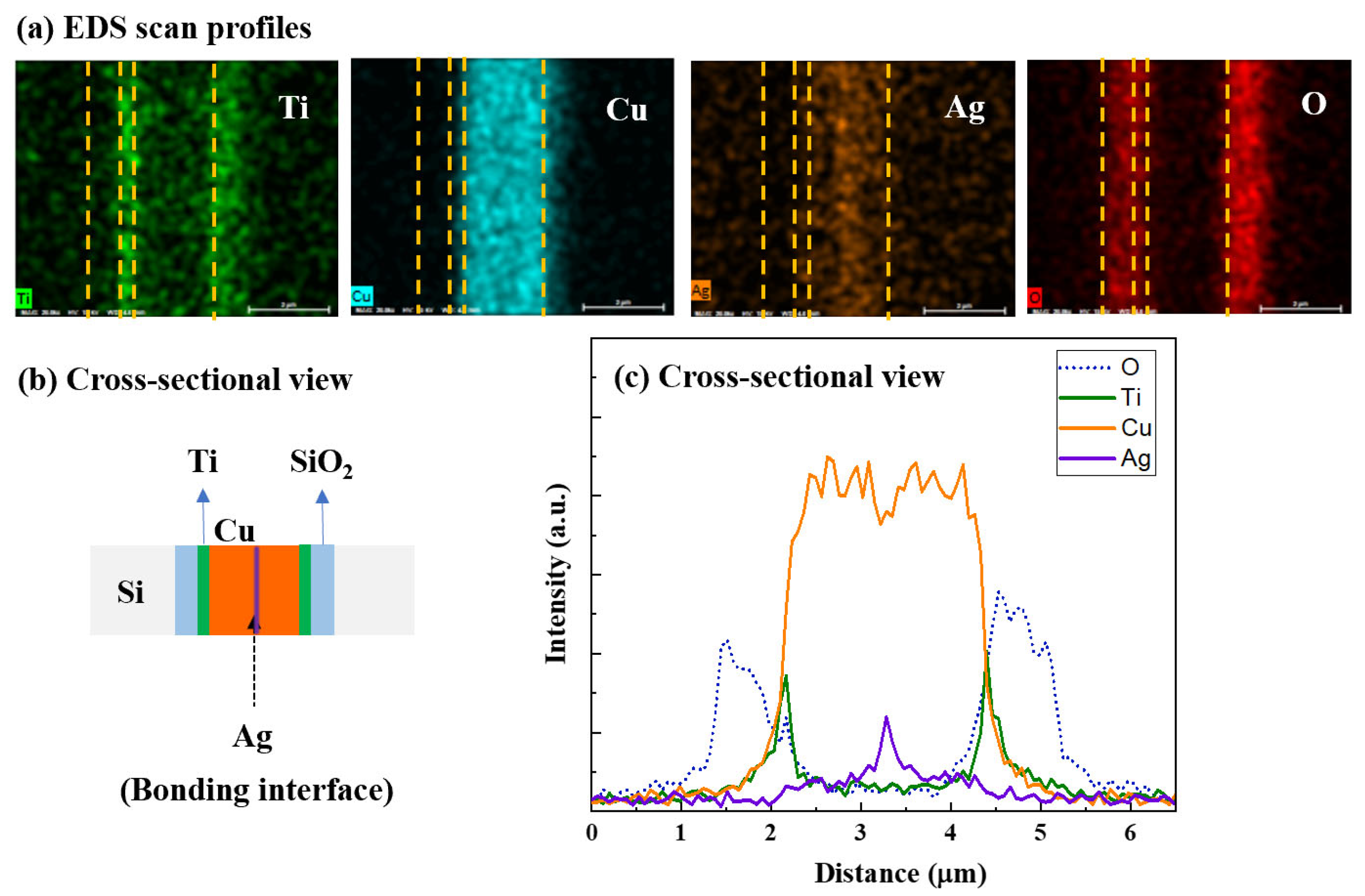
The two Cu samples with an Ag nanofilm were bonded at the temperatures of 150 °C and 180 °C under 30 MPa pressure in air using a heating press. After bonding, cross-sectional observation was undertaken by FIB-SEM, and elemental analysis was performed with EDS. For both the 150 °C and 180 °C bonding cases, a seam was observed at the bonded interface without voids, as shown in the FIB-SEM cross-sectional images of Figure 4. According to the inset images in Figure 4, this seam at the bonded interface was not a physically separated space. Rather, it appears that the Ag nanofilm was slightly etched off at the interface during the sample preparation by the FIB process. This was confirmed by the EDS measurements, shown in Figure 5, where Ag diffused into Cu but still remained at the bonded interface. In addition, Cu was observed at the bonded interface.
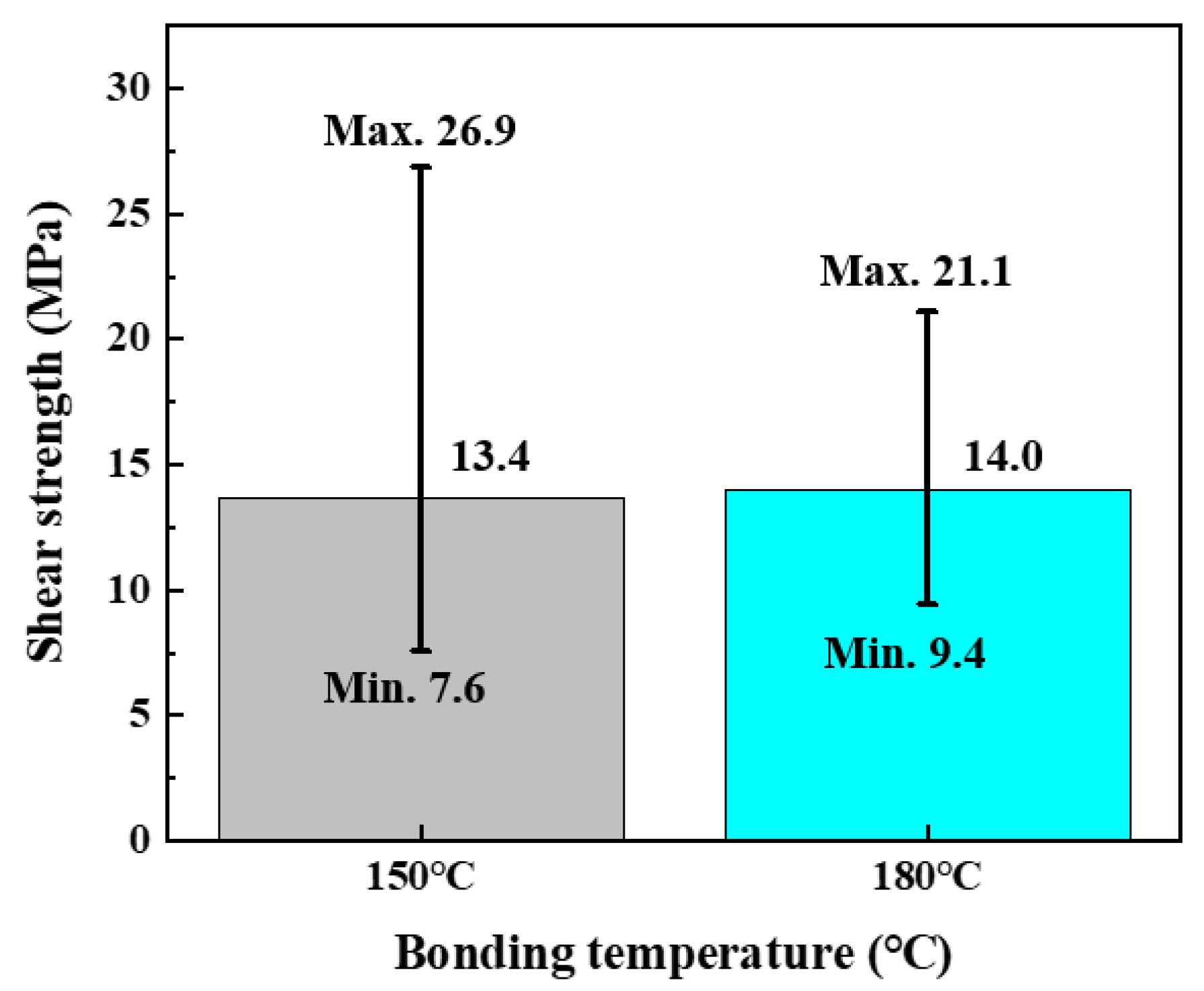
For quantitative analysis of bonding quality, the bonded samples were cut into 2 × 2 mm, and a shear test was performed with a 600 µm/sec tool tip speed. The shear test was taken as the average value after ten or more measurements and is shown in Figure 6. Some of the samples broke before Cu bonding interface separation, and some were SiO2/Ti-interface separated. In both cases, the other weak interfaces were separated prior to the Cu bonding interface. For the estimation of shear strength, the samples that were broken at the Cu bonding interface were considered. The average shear strength of Cu/Ag-Ag/Cu bonding was 13.4 MPa for 150 °C bonding and 14.0 MPa for 180 °C bonding. In both cases, there was little difference in average shear strengths, but the bonding at 150 °C showed a larger shear strength deviation than that of the bonding at 180°, as shown in Figure 6. It can be seen that the bonding at 180 °C has better reproducibility and uniform bonding than those of the bonding at 150°. In addition, the shear strength of broken or separated samples at other interfaces was as high as 35.9 MPa, which was often higher than the estimated average shear strength of 14.0 MPa. Therefore, although there was no annealing process in this study, it is expected that the bonding quality can be uniformly improved if a sufficient annealing process is performed after the Cu/Ag-Ag/Cu bonding of 30 min in order to activate further Ag diffusion.
The bonded interface was further analyzed by the TEM measurements. Figure 7 shows the TEM images and EDS profile across the interface of the Cu bonding at 180 °C. As shown in Figure 7, the bonding interface was well bonded, and the tiny voids visible at the interface were caused by the FIB process during the TEM specimen preparation. After 30 min of bonding at 180 °C, most Ag remained at the bonding interface, and some Ag diffusion into Cu was observed in the area in contact with the copper grain boundary.

4. Conclusions

Low-temperature Cu bonding with an Ag nanofilm was investigated. Cu/Ag-Ag/Cu bonding was performed below 200 °C, resulting in a good bonding interface and a shear strength of 14 MPa at 180 °C. A 15 nm Ag nanofilm effectively prevented Cu surface oxidation, but Ag remained at the bonded interface following low-temperature bonding. Cu/Ag-Ag/Cu solid state diffusion bonding should be further studied to achieve a complete solid solution of Ag into Cu at low temperatures. In addition, it is necessary to evaluate annealing after bonding to further improve bonding quality.

Author Contributions

Conceptualization, S.E.K.; Methodology, Y.K., and S.P.; Validation, Y.K., S.P., and S.E.K.; Formal analysis, Y.K.; Investigation, Y.K., and S.P.; Data curation, Y.K., and S.E.K.; Writing—original draft preparation, Y.K., and S.E.K.; Writing—review and editing, S.E.K.; Visualization, Y.K.; Supervision, S.E.K.; Funding acquisition, S.E.K. All authors have read and agreed to the published version of the manuscript.

Funding

This research was partly supported by the Basic Science Research Program through the National Research Foundation of Korea (NRF) funded by the Ministry of Science and ICT (NRF-2018R1A2B6003921) and the Korea Institute for Advancement of Technology (KIAT) grant funded by the Korean Government (MOTIE) (P0008458, The Competency Development Program for Industry Specialist).

Institutional Review Board Statement

Not applicable.

Informed Consent Statement

Not applicable.

Conflicts of Interest

The authors declare no conflict of interest.

References

  1. Panigrahi, A.K.; Chen, K.N. Low Temperature Cu-Cu Bonding Technology in 3D Integration: An Extensive Review. J. Electron. Packag. 2017, 140, 010801. [Google Scholar] [CrossRef] [Green Version]
  2. IEEE Heterogeneous Integration Roadmap: Chapter 21 SiP and Module System Integration and Chapter 22 Interconnects for 3D and 3D Architectures. 2020. Available online: https://eps.ieee.org/images/files/HIR_2019/HIR1_ch21_sip-module.pdf (accessed on 3 September 2021).
  3. Park, H.; Seo, H.; Kim, S.E. Anti-oxidant copper layer by remote mode N2 plasma for low temperature copper–copper bonding. Sci. Rep. 2020, 10, 21720. [Google Scholar] [CrossRef] [PubMed]
  4. Tan, C.S.; Lim, D.F.; Ang, X.F.; Wei, J.; Leong, K.C. Low temperature Cu-Cu thermo-compression bonding with temporary passivation of self-assembled monolayer and its bond strength enhancement. Microelectron. Reliab. 2012, 52, 321–324. [Google Scholar] [CrossRef]
  5. Hu, L.; Goh, S.C.K.; Tan, C.S. Ar/N2 Plasma Induced Metastable CuxNy for Cu-Cu Direct Bonding. ECS Trans. 2020, 98, 203–210. [Google Scholar] [CrossRef]
  6. Park, H.; Kim, S.E. Two-Step Plasma Treatment on Copper Surface for Low-Temperature Cu Thermo-Compression Bonding. IEEE Trans. Compon. Packag. Manuf. Technol. 2018, 10, 332–338. [Google Scholar] [CrossRef]
  7. Park, H.; Seo, H.; Kim, Y.; Park, S.; Kim, S.E. Low Temperature (260 °C) Solderless Cu-Cu Bonding for Fine Pitch 3D Packaging and Heterogeneous Integration. IEEE Trans. Compon. Packag. Manuf. Technol. 2021, 11, 565–572. [Google Scholar] [CrossRef]
  8. Huang, Y.; Chien, Y.; Tzeng, R.; Shy, M.; Lin, T.; Chen, K.; Chiu, C.; Chiou, J.; Chuang, C.T.; Hwang, W.; et al. Novel Cu-to-Cu Bonding with Ti Passivation at 180 °C in 3-D Integration. IEEE Electron Dev. Lett. 2013, 34, 1551–1553. [Google Scholar] [CrossRef]
  9. Panigrahi, A.K.; Bonam, S.; Ghosh, T.; Singh, S.G.; Vanjari, S.R.K. Ultra-thin Ti Passivation mediated breakthrough in high quality Cu-Cu bonding at low temperature and pressure. Mater. Lett. 2016, 169, 269–272. [Google Scholar] [CrossRef]
  10. Bonam, S.; Panigrahi, A.K.; Kumar, C.H.; Vanjari, S.R.K. Interface and Reliability Analysis of Au-Passivated Cu–Cu Fine-Pitch Thermocompression Bonding for 3-D IC Applications. IEEE Trans. Compon. Packag. Manuf. Technol. 2019, 9, 1227–1234. [Google Scholar] [CrossRef]
  11. Chou, T.; Huang, S.; Chen, P.; Hu, H.; Liu, D.; Chang, C.; Ni, T.; Chen, C.; Lin, Y.; Chang, T.; et al. Electrical and Reliability Investigation of Cu-to-Cu Bonding with Silver Passivation Layer in 3D Integration. IEEE Trans. Compon. Packag. Manuf. Technol. 2020, 11, 36–42. [Google Scholar] [CrossRef]
  12. Liu, Z.; Cai, J.; Wang, Q.; Wang, Z.; Liu, L.; Zou, G. Thermal-stable void-free interface morphology and bonding mechanism of low-temperature Cu-Cu bonding using Ag nanostructure as intermediate. J. Alloys Compd. 2018, 767, 575–582. [Google Scholar] [CrossRef]
  13. Liu, Z.Y.; Cai, J.; Wang, Q.; Tan, L.; Hu, Y. Low temperature Cu-Cu bonding using Ag nanostructure for 3D integration. ECS Solid State Lett. 2015, 4, 75–76. [Google Scholar] [CrossRef] [Green Version]
  14. Kim, Y.; Park, S.; Kim, S.E. Effect of Ag Nanolayer in Low Temperature Cu/Ag-Ag/Cu Bonding. J. Microelectron. Packag. Soc. 2021, 28, 59–64. (In Korean) [Google Scholar]
  15. Wang, M.Y.; Mei, Y.H.; Burgos, R.; Boroyevich, D.; Lu, G.Q. Effect of Substrate Surface Finish on Bonding Strength of Pressure-less Sintered Silver Die-attach. In Proceedings of the 2018 International Conference on Electronics Packaging and iMAPS All Asia Conference (ICEP-IAAC), Mie, Japan, 17–21 April 2018. [Google Scholar]
  16. Butrymowicz, D.B.; Manning, J.R.; Read, M.B. Diffusion in Copper and Copper Alloys Part ΙΙ. Copper-Silver and Copper-Colde Systems. J. Phys. Chem. 1974, 3, 533. [Google Scholar]
  17. Bokstein, B.S.; Vunkov, V.I.E.; Golosov, V.; Karpov, M.I.; Kolobov, Y.R.; Kolesnikov, D.A.; Korzhov, V.P.; Rodin, A.O. Structure and diffusion processes in laminated composites of a Cu–Ti system. Russ. Phys. J. 2009, 52, 811–815. [Google Scholar] [CrossRef] [Green Version]
Figure 1. Schematic diagram of the process flow.
Applsci 11 09444 g001
Figure 2. Equipment setup for the shear measurements.
Applsci 11 09444 g002
Figure 3. XPS depth profiles measured after heating for 1 h at 25 °C, 100 °C, and 150 °C: (a) Ag3d, (b) Cu 2p, and (c) O1s.
Applsci 11 09444 g003
Figure 4. FIB-SEM cross-sectional images of Cu/Ag-Ag/Cu bonded samples.
Applsci 11 09444 g004
Figure 5. EDS measurements of Cu/Ag-Ag/Cu bonding interface (sample bonded at 150 °C).
Applsci 11 09444 g005
Figure 6. Shear strength measurements of Cu/Ag-Ag/Cu bonded samples.
Applsci 11 09444 g006
Figure 7. TEM and EDS analysis of Cu/Ag-Ag/Cu bonding at 180 °C: (a) TEM image of bonding interface, (b) magnified TEM image of the red box, and (c) EDP profile across the interface.
Applsci 11 09444 g007
Table 1. Chip bonding conditions.
Temperature (°C)Pressure (MPa)Time (min)Annealing
1503030No
1803030No
Publisher’s Note: MDPI stays neutral with regard to jurisdictional claims in published maps and institutional affiliations.