
A New, Fast Pseudo-Random Pattern Generator for Advanced Logic Built-In Self-Test Structures


Division of Digital Systems, Faculty of Automatic Control, Electronics and Computer Science, Silesian University of Technology, 44-100 Gliwice, Poland
Appl. Sci. 2021, 11(20), 9476; https://doi.org/10.3390/app11209476
Submission received: 1 September 2021
/
Revised: 5 October 2021
/
Accepted: 6 October 2021
/
Published: 12 October 2021
(This article belongs to the Special Issue Energy, Area, and Speed—Efficient Digital Circuits)
Abstract
:Digital cores that are currently incorporated into advanced Systems on Chip (SoC) frequently include Logic Built-In Self-Test (LBIST) modules with the Self-Test Using MISR/Parallel Shift Register Sequence Generator (STUMPS) architecture. Such a solution always comprises a Pseudo-Random Pattern Generator (PRPG), usually designed as a Linear Feedback Shift Register (LFSR) with a phase shifter attached to the register and arranged as a network of XOR gates. This study discloses an original and innovative structure of such a PRPG unit referred to as the DT-LFSR-TPG module that needs no phase shifter. The module is designed as a set of identical linear registers of the DT-LFSR type with the same primitive polynomial. Each register has a form of a ring made up exclusively of D and T flip-flops. This study is focused on the investigation of those parameters of DT-LFSR registers that are essential to use these registers as components of PRPG modules. The investigated parameters include phase shifts and the correlation between sequences of bits appearing at outputs of T flip-flops, implementation cost, and the maximum frequency of the register operation. It is demonstrated that PRPG modules of the DT-LFSR-TPG type enable much higher phase shifts and substantially higher operation frequencies as compared to competitive solutions. Such modules can also drive significantly more scan paths than other PRPGs described in reference studies and based on phase shifters. However, the cost of the foregoing advantages of DT-LFSR-TPG modules is the larger hardware overhead associated with the implementation of the solution proposed.
1. Introduction
Digital cores that are currently incorporated into advanced and up-to-date Systems on Chip (SoC) usually include Logic Built-In Self-Test (Logic BIST, LBIST) modules. A very popular LBIST architecture operated in the test-per-scan mode is STUMPS (Self-Test Using MISR/Parallel Shift register sequence generator) [1,2] (pp. 288–290), [3] (pp. 176–177), [4] (pp. 522–525), or various versions of it [5,6,7,8,9]. The structural diagram of a typical LBIST module with the STUMPS architecture as depicted in Figure 1 includes some key components, such as a generator of pseudo-random tests, or more specifically, a Pseudo-Random Pattern Generator (PRPG) and a Multi-Input Signature Register (MISR). The PRPG module is intended to supply pseudo-random sequences of bits simultaneously to all scan paths of a circuit to be tested, and these sequences are then delivered as parallel test vectors to inputs of combinational logic blocks of such a Circuit Under Test (CUT). A PRPG module is usually designed as a shift register with linear feedback (Linear Feedback Shift Register—LFSR) [3] (pp. 65–71, 176–177), although Cellular Automata (CA) can also be used for these purposes [3] (pp. 72–75), [10,11,12,13]. Some specific solutions may also comprise other types of linear registers such as PRPG modules, for instance Galois Linear Feedback Shift Register (GLFSR) [14,15,16]. Responses to test vectors gathered from outputs of a CUT are loaded in the parallel mode into scan paths, and then scan paths are switched to the serial mode and information from all scan paths is supplied to inputs of the MISR module where information is subject to compaction (lossy compression). The final content of the MISR is referred to as the signature, which provides information on whether the CUT is faulty or not. The substantial advantage of LBIST structures with the STUMPS architecture consists of the fact that such solutions offer much shorter testing times as compared to conventional built-in self-test solutions operated in the test-per-scan mode since pseudo-random sequences of bits are supplied simultaneously to a plurality of scan paths [3] (pp. 176–177). Although STUMPS architecture appeared as early as the 1980 s, it is still quite popular and constantly in use. There are numerous studies where researchers make efforts to improve the solution in terms of hardware overhead, testing time, power consumption, fault coverage, diagnosability, etc. [17,18,19,20,21,22,23,24,25,26]. Some variations of the STUMPS architecture are implemented into hybrid LBIST, where pseudo-random testing is combined with deterministic testing or test data compression [27,28,29,30,31,32].
The remainder of this study shall have the following structure. Section 2 deals with some problems with fault coverage that may happen to basic options of the LBIST structure with the STUMPS architecture and explains the reasons for such problems. Section 3 outlines how PRPG modules are usually designed to remedy the aforementioned problems. New concepts for the implementation of PRPG modules into LBIST circuits with the STUMP architecture are shown in Section 4, where the implementation of specific DT-LFSR ring linear registers is proposed. The innovative structure, operation principle, and key properties of DT-LFSR Test Pattern Generators (DT-LFSR-TPG), designed according to the concept shown in previous sections, are brought together in Section 5. The logical synthesis results of the new type of pseudo-random pattern generators are presented in Section 6. The study ends up in Section 7 with a discussion of the results obtained, recapitulation, and key conclusions.
2. Motivation
Requirements that are imposed to any Test Pattern Generator (TPG) usually include on one hand the need to guarantee a high coverage factor of faults that may occur in a CUT and, on the other hand, the acceptable testing time. Pseudo-random TPGs are frequently designed as conventional Linear Feedback Shift Registers (LFSR) based on primitive polynomials. The main cycle of the state diagram of such an n-bit register contains all 2n − 1 states except for the vector <00…0>. In addition, every LFSR register produces identical sequences of bits at each of its outputs, and these sequences are merely mutually shifted in phase. Every single sequence is of the pseudo-random nature, i.e., meets the requirements stipulated in [33] for pseudo-random binary sequences. Unfortunately, in spite of the foregoing properties attributable to conventional LFSRs, implementation of them as generators of pseudo-random test patterns may entail some problems with the fault coverage, which is strongly manifested for the STUMPS-type LBIST architecture. Namely, when a conventional LFSR with an external feedback loop (type I LFSR [34]) is implemented as a TPG into the mentioned LBIST architecture, some faults in the CUT may remain undetected due to an insufficient phase shift between bit sequences supplied to scan paths. The foregoing problem is illustrated by the example below.
- Example 1
Figure 2 depicts a fragment of a circuit to be tested by means of five scan paths. Serial inputs of these scan paths are fed from parallel outputs of a five-bit type I LFSR designed for the primitive polynomial . Outputs of that register produce identical pseudo-random sequences of bits but with a sequential phase shift. The figure depicts an example of content in the scan paths and the register, whilst dotted lines indicate interrelationships between contents of individual scan paths. Outputs of these scan paths cells feed inputs of exemplary gates included in the CUT (gates G1–G4). To make the picture more clear, the remaining part of the CUT, where outputs of the mentioned gates are wired, is not shown in the figure.
The foregoing example demonstrates that the following faults of the CUT are not detectable: stuck-at-1 at the output of the OR (G2) gate, stuck-at-0 at the output of the XOR (G4) gate, short (bridging fault) between inputs of the AND (G3) gate as well as an open break at the input of the CMOS transistor with the p channel (input A) within the NOR (G1) gate. The reason why those faults are undetectable lies in insufficient phase shift, actually equal to 1, between binary sequences produced at adjacent outputs of the TPG. Due to such an insufficient phase shift the content of both the j + kth and jth cells in the scan paths wired to respective ith and i + kth outputs of TPG shall be always equal to another (i = 0, 1,…, n − 2, j = 0, 1,…, L − 2, k = 1, 2,…, i + k < n, j + k < L), where n stands for the length of the TPG and L is the length of scan paths (for the example in question n = 5, L = 8). Therefore, the “00” pair of bits shall never appear at the A and B inputs of gate G2, which is mandatory to switch the gate output over to the state that is opposite to the fault, i.e., to zero. Likewise, it is also infeasible to deliver such combinations as AB = 01 or AB = 10 to inputs of the G4 gate, which is necessary to set the gate output to “1”. Moreover, both inputs of the G3 gate are always equal, so they appear to be shorted, and that makes it infeasible to detect the type of the actual fault. In turn, the detection of a fault affecting the G1 gate needs to deliver the test vector sequence “00,10” to the AB inputs. Since inputs of that gate also always adopt the same state during the entire testing process, the aforementioned sequence shall never occur.
The issue disclosed in Example 1 can be formulated in a more general way; i.e., a low phase shift between test bit sequences appearing at neighboring outputs of a pseudo-random TPG leads to a strong correlation between test vectors supplied to scan paths fed from these outputs. It is why these vectors may no longer be considered as pseudo-random ones, which adversely affects the fault coverage in digital CUTs with the STUMPS-type LBIST architecture [3] (pp. 177–181), [12,34,35,36,37]. In addition, page 322 in [38] shows an example to demonstrate that test vector sequences generated by an I-type LFSR and feeding parallel inputs of a circuit tested in the test-per-clock mode shall be incapable of detecting some faults in the digital circuit under test.
The concept of output channels from a Test Pattern Generator (TPG) frequently appears in reference studies. These channels are actually numerous scan paths fed from outputs of the TPG. The phase shift between binary bitstreams supplied to individual scan paths is also referred to as the separation factor between data channels or between scan paths’ content [3] (pp. 184–188), [13,14,34,37,39].
The low phase shift between bit sequences appearing at outputs of the type I LFSR register and their strong mutual correlation is also confirmed by the State-Time Diagram (STD) that depicts the sequence of test vectors produced by such a shift register [10]. For such an illustration of test vectors, each “0” appearing at any output of the register is represented by a white dot, whilst black dots stand for high (“1”) values of outputs.
Figure 3a shows an example of a 20-bit type I LFSR associated with the primitive polynomial and a fragment of the STD graph for that register is depicted in Figure 3b. The Q0 output of the register corresponds to dots at the top of the graph, while the Q19 output is associated with dots in the graph bottom. The time axis for the register operation extends horizontally.
The register starts its operation from the state of <1000…00>. The STD graph from Figure 3b features with pretty regular shape since it has the form of oblique white and black stripes. One can easily spot that sequences of bits appearing at subsequent outputs of the LFSR register are gradually shifted by only one bit. Likewise, subsequent vectors appearing at outputs of that register are also gradually shifted by only one bit (except for the bit number 0). These properties indicate a strong correlation both between binary sequences and between subsequent vectors appearing at outputs of the LFSR register [10,12,35]. As a consequence, sequences of test vectors produced by such a register must not be considered as fully pseudo-random ones, both for the test-per-scan and test-per-clock testing strategies [10,40]. Similar observations are reported in [38] with respect to poor randomness of test vectors sequences delivered at outputs of a conventional LFSR.
The strong correlation between sequences of test bits appearing at outputs of the type I LFSR is also confirmed by the graph plotted in Figure 4 for the correlation coefficient. The correlation coefficient for binary sequences is calculated from the formula [33]:
where and stand for the values of the corresponding ith and jth outputs of the register at the moment of t, while , and is the length of binary sequences used to calculate the correlation coefficient. The parameters of represent the time offset (phase shift) between binary sequences at the outputs and , where test sequences are observed and the difference between indexes and is considered as the space distance between these two sequences. When the function calculates the autocorrelation coefficient for the binary stream appearing at the qi output. For all other cases, i.e., when , the function calculates the coefficient of cross correlation between binary sequences produced at the outputs and . That coefficient can be calculated either for the entire period of the register operation, in which in Equation (1), or for the actual length of the test sequence. It must be also kept in mind that for computation of the correlation coefficient by means of the equation (1) all parameters qi(t) = 0 shall be substituted with the values of “−1” [33].
In the graph depicted in Figure 4, the horizontal axes show the time offset τ expressed in the number of clock cycles (the axis designated as “time offset τ”) as well as space distance, understood as the number of the register output (the axis designated as “output no”). In turn, the vertical axis (“correlation coefficient”) is graduated with the values of correlation coefficients. The coefficient is calculated with respect to the binary sequence appearing at the q0 output with no time offset. The graph presented in Figure 4 demonstrates that in the case of a conventional type I LFSR register, the coefficient of correlation between the binary sequence appearing at the qi output and the corresponding sequence at the q0 output but delayed by i clock cycles adopts the maximum value, i.e., equals 1. On the other hand, the correlation coefficient between a bit sequence at any of the qi outputs and the bit sequence at the q0 output and delayed by j clock cycles, where j ≠ i, adopts really small values and ranges from −0.02 to 0.02, which is shown in Figure 5.
As mentioned before, not only the LFSR register can be applied as a PRPG with the LBIST arrangement and the STUMPS architecture, but linear registers of the CA or GLFSR can be used as well. The most frequent design option of the CA register is the one-dimensional Linear Hybrid Cellular Automata (LHCA) with null boundary conditions, made up of cells with the rules 90 and 150 [10,12,41,42,43,44]. In a later part of this study, such a design option of the CA register shall be designated as LHCA 90/150. The reference literature also reports the application of two-dimensional LHCA to LBIST solutions, where a portion of cells is interconnected with at least three neighboring cells [45,46,47,48]. Additionally, the concept of the TPGs design as an LHCA with the hierarchical structure was developed [49]. However, all the aforementioned solutions suffer from some drawbacks that are discussed below.
The [12] reports that the separation coefficient between output channels of the LHCA 90/150 adopts pretty different values, and some of these values are very low. In addition, the information only about the configuration of the LHCA 90/150 register is insufficient for an unambiguous indication of the register outputs affected by the mentioned problem. The foregoing observation is also confirmed in [14], even with an additional conclusion that the problem with insufficient separation between a portion of output channels relates to as much as about 75% of structures developed for LHCA 90/150 registers associated with primitive polynomials. Similarly, two-dimensional Tree-structured Linear Cellular Automata (TLCA) also exhibited very low values of the phase shift between a portion of bit sequences appearing at outputs of the register [46].
In the case of two-dimensional LHCAs, at least some cells are interconnected with outputs of more than two neighboring cells [45,47,48]. Therefore, these cells comprise at least two XOR gates that are arranged in series. The need to use multi-layered networks of XOR gates is also a drawback of CA solutions with hierarchical structures [49]. Likewise, a portion of wires in the linear feedback of a GLFSR register requires a serial arrangement of XOR gates used as so-called multiplying units and other XOR gates, which are the so-called adding units [16]. Eventually, the need to use at least two-layered networks of XOR gates in feedback lines of the aforementioned linear registers mitigates the maximum operation frequency of such solutions.
The use of CA or GLFSR structures as PRPGs in LBIST circuits with the STUMP architecture needs the determination of phase shifts between individual bit sequences appearing at outputs of such registers. Some methods that have been applied for that purpose are actually based on simulation of CA or GLFSR modules by means of matrix operations and seeking adequate states of the register where single bits are set to “1” [43,50]. However, such methods are very time-consuming, which is confirmed in [12], where the algorithm developed in [50] is applied. Due to the very long computation time necessary to find out phase shifts between binary sequences at outputs of the LHCA 90/150 structures, the overall length of CA registers investigated in the mentioned study had to be limited. In turn, studies [11,51] report the application of an algebraic method based on discrete logarithms [52,53] (pp. 97–111) to compute the phase shifts. Unfortunately, all algorithms that are suitable for the calculation of discrete logarithms [53] (pp. 97–111) are very complex, and the application of the mentioned methods is practically limited to linear registers of a relatively short length.
3. Classical Method to Design LBIST Circuits with the STUMPS Architecture
The previous chapter outlines reasons that prevent us from achieving high coverage of faults in CUTs that are provided with LBIST circuits with the STUMPS architecture. These problems stem from the low phase shift between binary sequences appearing at outputs of pseudo-random TPGs that are designed exclusively on the basis of a conventional LFSR structure associated with a primitive polynomial. This is why a phase shifter [3] (pp. 184–188), [54] is usually inserted between outputs of the LFSR [34,35,36,37,55] or LHCA 90/150 [12,37,39,55,56] and serial inputs of scan paths incorporated into the CUT. Such a modified STUMPS architecture is shown in Figure 6. In a later part of this study, the TPG provided with a phase shifter at its outputs shall be referred to as a test pattern generator based on LFSR or CA with Phase Shifter at the outputs and designated as LFSR + PS and CA + PS, respectively. The phase shifter itself is a network of XOR gates appropriately wired to outputs of the LFSR or CA register.
Its application not only makes it possible to provide sufficient phase shift between binary sequences supplied to serial inputs of scan paths but also enables incorporation of LFSR structures of much lower size than the number of scan paths ( in Figure 6). For instance, in [34], the authors used LFSR registers with lengths of 24, 32, 48, 64, 80, 96, and 128 bits to produce test sequences supplied then to multiple scan paths, where the number of scan paths fed from a single TPG ranged from several dozens to more than 8000. However, the use of a phase shifter inevitably entails a delay introduced into the hardware, which is a drawback of the proposed solution. The time of signal propagation throughout the phase shifter is several times longer than the propagation time of multiplexers incorporated into scan path cells [34], and, in addition, that time is added to the propagation time of the multiplexer embedded into the first cell of a scan path. These two factors restrict the maximum operation frequency of the test facilities made up of TPG and scan paths. It eventually leads to an extended total time of test execution.
In addition, when a single LFSR feeds a plurality of scan paths, things get worse due to the need to route interconnections within a sophisticated network of XOR gates incorporated into a phase shifter. Typically, the desired fan-out factor is achieved by incorporation of additional buffers (logic amplifiers) wired to the flip-flops’ outputs of the LFSR and to some XOR gates outputs of the phase shifter. These two factors lead to further growth of propagation time for signals passing the phase shifter and make the engineering process for test pattern generators much more complicated.
The studies referenced disclose several methods to design phase shifters with the aim to ensure the assumed value of the phase shift between output data channels. Some of these methods are based on operations on digital matrices that describe structures of linear registers and phase shifters connected to the LFSR or CA outputs [37,57]. Other solutions employ simulation of a linear register operation, where the simulated linear register structure reflects the layout of an original linear register combined with a phase shifter. However, it is an approach that may prove time-consuming in the case of long linear registers [34,35,36,39,56]. Additionally, other methods have been developed intending to find out such structures of both an LFSR register and a phase shifter that are capable of generating the desired set of deterministic test vectors [22,58].
4. New Approach to Engineering of Pseudo-Random Pattern Generators for LBIST Circuits with the STUMPS Architecture
The engineering concept disclosed in this chapter is based on the application of DT-LFSR (Linear Feedback Shift Register composed of D- and T-type flip-flops) shift registers with a linear feedback [38,59] to new types of pseudo-random TPGs for LBIST circuits with the STUMPS architecture. However, before the structure of the innovative TPG is revealed, let us outline some selected properties of DT-LFSR registers.
4.1. Layout of a DT-LFSR Register
Any DT-LFSR is designed as an endless ring of D and T flip-flops connected in series. The principal schematic of an n-bit DT-LFSR register comprising flip-flops of the D type and flip-flops of the T type is depicted in Figure 7. In this study, such a structure of a DT-LFSR register shall be symbolically designated as DkTt. Attention should be paid to the fact that such a register contains no XOR gates in the main loop of the linear feedback. Instead, it contains XOR gates in internal linear feedback loops inside T-flip-flops. A T-type flip-flop is actually a D-type flip-flop with an XOR gate in a feedback loop. Therefore, the characteristic polynomial that corresponds to the linear feedback of an n-bit DT-LFSR from Figure 7 adopts the following form:
where It is important to mention that any rearrangement of the register layout with reordering of the D and T flip-flop sequence in the ring register has no effect on the characteristic polynomial of that register. Relocation of T-type flip-flops in such registers can be actually considered as a sequence of left shift operations applied to local linear feedback loops. Such a procedure was named in [60] as the EL transformation. According to Theorem 1 disclosed in that study, such modifications of linear register structures are indifferent to the characteristic polynomial of the register.
It is also worth mentioning that a DT-LFSR register is actually a specific variation of Linear Hybrid Cellular Automata (LHCA) with cyclic boundary conditions, made up of cells with the rules 60 and 240. Each T-flip-flop is a CA cell with the rule 60 while a D-flip-flop is a CA cell with the rule 240. A table summarizing all possible structures of DT-LFSR registers with the length of and a linear feedback loop described by means of a primitive polynomial can be found in some past papers, including [38]. The table content serves as the proof that for the specific length n of a DT-LFSR register only some combinations of k and t parameters lead to such a DkTt structure of the register that corresponds to a primitive characteristic polynomial. Each of these structures contains at least one D-type flip-flop (i.e., k > 0 for every case). In addition, for some specific lengths of registers, any DT-LFSR structure associated with a primitive characteristic polynomial may not exist.
4.2. Correlations between Binary Sequences at Outputs of T-type Flip-Flops Incorporated into DT-LFSRs
Section 2 discloses the STD graph for the sequence of test vectors and the graph of the correlation coefficient for binary sequences appearing at outputs of a conventional 20-bit type I LFSR register. These parameters are deemed as the key quality indices for a register operated as a generator of pseudo-random sequences of test vectors. These two graphs for the DT-LFSR register with the D3T17 structure (see Figure 8a), associated with the primitive polynomial: , are depicted in respective graphs in Figure 8b and Figure 9.
The STD graph for the aforementioned register is less regular than the graph for a conventional LFSR structure since oblique stripes, typical for conventional LFSR registers, are seen only in the areas that correspond to D-type flip-flops. Instead, in areas corresponding to T-type flip-flops, white triangle-shaped patterns can be seen at random locations. The foregoing observations are coherent with the findings reported in [38] with regard to test vector sequences generated by linear feedback registers with T-type flip-flops. In turn, the graphs for correlation coefficients clearly indicate that only the binary sequences appearing at outputs of D-type flip-flops are strongly correlated. On the other hand, the correlation coefficient for binary sequences produced at outputs of T-type flip-flops ranges from −0.02 to 0.02 (see Figure 10); i.e., it is extremely low.
4.3. Phase Shifts between Binary Sequences at Outputs of T-type Flip-Flops Incorporated into DT-LFSRs
This section is dedicated to investigating phase shifts between bitstreams at the outputs of D- and T-type flip-flops in the DT-LFSR type ring registers. Let us consider an n-bit register with the DkTn−k structure and associated with the primitive polynomial . Let us also denote the phase shift introduced by D-type and T-type flip-flops present in that register as and respectively. The analysis carried out in [38] makes it possible to find out that while the phase shift can be calculated from the following congruence:
Please note that the phase shift is identical for all D-type flip-flops incorporated into the DT-LFSR structure; likewise, the phase shift is the same for all T-type flip-flops within that register. In addition, the congruence (3) indicates that for every n > 1. According to Corollary 2 in [53] (p. 20), when g.c.d. (, the solution of the Equation (3) always exists, and the solution can be found by means of binary operations. In practice, for the example when and , the solution of the Equation (3) was found in less than 4 s with the use of a calculator available online [61]. The n and k parameters provided in that example correspond to the only D63T37 structure of a DT-LFSR register with the length of 100 bits that is associated with a primitive polynomial.
- Example 2
Figure 11 shows a sequence of test vectors produced by a register of the DT-LFSR type with the D1T2 structure. That register is associated with the primitive polynomial Therefore, the respective coefficients are and . For the example in question, the congruence (3) adopts the following form:
which indicates that the phase shift introduced by the T-type flip-flops is . Obviously, the phase shift introduced by D-type flip-flop is .
The magnitude of phase shift between binary sequences produced at the adjacent outputs of the foregoing DT-LFSR register with the D1T2 structure is explained in Figure 11, where arrows indicate corresponding bits in mutually shifted binary sequences. To make the picture more clear, the binary sequence appearing at the Q2 output is repeated at the left-hand side of the binary sequence produced at the Q0 output. In addition, the numbering of clock cycles is shown in the leftmost part of the figure for easy calculation of the phase shift.
The congruence (3) also enabled calculation of the phase shift for DT-LFSRs with the length exceeding 24 bits and containing a considerable number of T-type flip-flops (more than 80% of the total register length). Results of these calculations are summarized in Table 1, where the overall number of T-type flip-flops within each specific register and the total length of the register are provided in columns 2 and 3 of that table, respectively, column 4 specifies the duration (length) of the operation cycle for each specific register, and column 5 contains the parameters, i.e., the phase shift between binary sequences appearing at the output and the input of a T-type flip-flop within the DT-LFSR register in question.
Now let us assume that an n-bit register of the DT-LFSR type contains flip-flops of the T type that are deployed in register cells with the numbers . Let us also denote as the phase shift between binary sequences produced at the outputs and of the register in question, where ; i.e., it is a phase shift between binary sequences appearing at outputs of two selected T-type flip-flops within the register. The phase shift is then
where stands for the aforementioned duration of the operation cycle for the DT-LFSR register. For negative numbers, the operation mod appearing in (5) is calculated according to the formula . Please note that the phase shift is calculated as modulo , and thus it can be less than . Therefore, let us define the minimum phase shift——between binary sequences produced by two discretely selected T-type flip-flops of the DT-LFSR registers. Such a minimum phase shift is defined by the following equation:
The minimum phase shift for some selected DT-LFSR registers are summarized in column 6 of Table 1. The foregoing deliberations take account of binary sequences merely at outputs of T-type flip-flops since only these flip-flops introduce a phase shift that is different from 1. Therefore, only the outputs of T-type flip-flops can be exclusively used as outputs of a Test Pattern Generator.
5. Pseudo-Random Pattern Generator DT-LFSR-TPG for LBIST Circuits with the STUMPS Architecture
Let us denote as the minimum guaranteed phase shift between binary sequences produced at outputs of any TPG applicable for the STUMPS architecture. Results from Table 1 demonstrate that a single DT-LFSR register used as a pseudo-random TPG enables a pretty high level of phase shift that is much more than the one achieved by means of the methods disclosed in [13,34,35,39].
The number of scan paths implemented in LBIST structures with the STUMPS architecture and incorporated into modern integrated circuits is as high as several thousand [25]. The implementation of a PRPG as such a long and single DT-LFSR register is a sophisticated engineering challenge. There are difficulties associated with development for the register topology as well as a network of interconnections between its cells and a network of interconnections between the register outputs and inputs of scan paths so as to achieve the desired operational frequency of such a TPG. The next problem is associated with seeking an appropriate DkTt structure associated with a primitive polynomial with the length of several thousand bits. The verification of whether the characteristic polynomial of such a register is really a primitive one can be carried out by means of the efficient algorithm proposed in [39,62]. However, such a solution needs prime factorization of a very large number expressed as , where stands for the length of the DT-LFSR register.
The aforementioned problems can be resolved by means of the original method and the innovative method outlined in this paper dedicated to the implementation of PRPG structures as a set of DT-LFSR registers operated in the parallel mode. The STUMPS architecture with a TPG designed according to the foregoing concept is depicted in Figure 12. All DT-LFSR registers of such a test pattern generator are of identical design and are synchronized by means of a common clock signal and their operation is controlled simultaneously by the same control signals. Outputs of T-type flip-flops incorporated into each single register deliver sequences of test vectors to a separate group of scan paths, whilst outputs of D-type flip-flops remain unused, which is indicated in the sketch below. A Test Pattern Generator with such a structure shall be further referred to as DT-LFSR-TPG.
According to [34,35], the minimum phase shift between binary sequences produced at any two outputs of a future TPG is imposed a priori before the engineering of a pseudo-random TPG for the STUMPS architecture is commenced. The sufficient level of that phase shift is deemed as a guarantee that a sequence of test vectors supplied to inputs of the CUT shall be of a pseudo-random nature. Any properly designed TPG must meet the condition that ; i.e., the minimum phase shift between binary sequences appearing at outputs of such a TPG must be not less than the required limit imposed by the circuit designer. To meet the foregoing requirement, each single-DT-LFSR register incorporated into the DT-LFSR-TPG structure of the TPG must start its operation from a different seeding vector (i.e., from a different initial state). Let us assume that the seeding content S1 of the DT-LFSR1 register is adopted as the reference point and let us also assume that such a seeding content appears in the sequence of vectors produced at outputs of the foregoing register in the clock cycle No. 0. Therefore, the seeding content Si of any DT-LFSRi register should be included in the initial sequence in clock cycle , where can be expressed by means of the following formula:
If so, binary sequences produced at the rth outputs of the DT-LFSR1 and DT-LFSRi registers, where , shall be mutually shifted with the phase shift of di clock cycles.
The maximum number of scan paths that can be wired to outputs of a TPG with the specific minimum limits for and shall be defined by Equation (8).
The maximum numbers calculated from the foregoing equation are summarized in Table 2, where columns 2 and 3 of the table contain parameters of DT-LFSR registers incorporated into the TPG. The number of scan paths for various is provided in columns 4 to 9. The are adequately selected so as to cover the range assumed in [34,39]. Please note that in cases when the presumed offset is known, Table 2 makes it possible to find out and parameters of the appropriate DT-LFSR register to enable designing of a TPG that is able to supply test sequences to any number of scan paths, or at least as many as practicable.
For comparison, Table 3 summarizes the maximum number of scan paths that were obtained in [34,39] for similar phase shifts as included in Table 2. The LFSR I and LFSR II symbols in the first column of the table correspond to the test pattern generator of the LFSR + PS type as outlined in [34], where the phase shifter is wired to outputs of LFSR registers of the respective I and II types. In turn, the LHCA 90/150 symbol stands for the generator of the CA + PS type designed to produce pseudo-random tests and including the LHCA 90/150 register and a phase shifter. In addition, Table 3 comprises results for two lengths of LFSR and LHCA 90/150 registers designed to control phase shifters, where the length (n) can be either or bits. The comparison between Table 2 and Table 3 clearly indicates that for the same separation between channels, the DT-LFSR-TPG is able to feed more or even sufficiently more scan paths than the solutions disclosed in [34,39]. It is only necessary to properly select the n and t parameters of the DT-LFSR register that is then used to design the DT-LFSR-TPG structure. For instance, all DT-LFSR registers with the n and t parameters listed in lines 5 to 24 of Table 2 make it possible to design a PRPG of the DT-LFSR-TPG type with the parameters that exceed the ones provided in Table 3.
To emphasize advantages of DT-LFSR-TPG structures, Table 4 summarizes the maximum number of scan paths that can be fed from a DT-LFSR-TPG structure for much higher phase shifts (separation offset between channels) than the ones considered in Table 2 and Table 3. Please note that when the phase shift is as high as tens of trillions of clock cycles, it is also possible to find a DT-LFSR register with appropriate n and t parameters to use it as the basis to design a DT-LFSR-TPG structure capable of feeding any number of scan paths.
Not only is essential for the engineering of a test pattern generator, but also the minimum phase shift between binary sequences supplied by the TPG to inputs of the predefined number of scan paths. The minimum phase shift is expressed by (9).
Table 5 summarizes parameters for various numbers of scan paths fed from the TPG, where the numbers of scan paths are almost identical to the ones in [34,39]. The analysis of the table contents makes it possible to conclude that for a specific number of scan paths a suitable DT-LFSR register can be selected so that the required phase shift can be assured. The maximum limit of the phase shift taken into account in studies [34,39] is On the contrary, the figures from Table 5 indicate that the phase shift (separation factor for output channels) enabled by the DT-LFSR Test Pattern Generator (DT-LFSR-TPG) for a specific number of scan chains can be higher by several magnitudes than numbers offered by LFSR + PS and CA + PS solutions disclosed in aforementioned studies.
6. Results of Logic Synthesis
Other parameters that are essential for any test pattern generator include the maximum operational frequency and the cost of hardware implementation, expressed, for instance, as the area of silicon surface occupied by the TPG or as the number of equivalent two-input NAND gates. The foregoing properties for the innovative type of DT-LFSR-TPG pseudo-random pattern generators were established from the logic synthesis of selected DT-LFSR registers. For that purpose, a parameterized model of a DT-LFSR register was developed in the VHDL language, where the general layout of the register is shown in Figure 13a. Besides D-type flip-flops and a 2 to 1 multiplexer, the register also comprises configurable D/T flip-flops with the internal structure as shown in Figure 13b. Corresponding to the input signal M, such a circuit can perform as a D-type flip-flop (for M = 0) or a T-type flip-flop (when M = 1). Variations of parameters for the VHDL model make it possible to set up both the register length and the number of configurable D/T flip-flops included in the register, while the MODE signal shown in Figure 13a is dedicated to controlling the operation mode for the entire DT-LFSR register module. For MODE = 1, the module operates as a DT-LFSR linear shift register, whilst setting the MODE signal to zero switches the module to operation as a shift register, and its initial content can be seeded by feeding a corresponding series of bits to its serial input SI. The module also has a serial output SO, which enables serial sequencing of DT-LFSR registers included in a large DT-LFSR-TPG unit, where the SO output of the ith register is connected to the SI input of the register with the number (), where , and stands for the total number of DT-LFSR registers included into the test pattern generator. When MODE = 0, all DT-LFSR modules make up a single and long shift register, which makes it possible to seed any initial content of that registers.
The logic synthesis of DT-LFSR registers was carried out with the use of the commercial software LeonardoSpectrum from Mentor Graphics, Wilsonville, OR, US (currently Siemens EDA), as well as the TSMC 0.25 µm standard cell library included in the ASIC Design Kit rev. 3.1, also made available by Mentor Graphics, Wilsonville, OR, US. The decision to use this particular standard cell library was triggered by the fact that the same technology, with 0.25 µm, was used in [34] for synthesis of phase shifters investigated in that study. It enables a reliable comparison of experimental results disclosed in the further part of this paper against the ones discussed in [34].
Nevertheless, it should be mentioned herein that the structure of the DT-LFSR register is ring-shaped; therefore, it enables substantial reduction of length for all interconnections between the register cells and, in consequence, delays caused by these interconnections. To achieve the most satisfying results for the DT-LFSR structure, it is recommended that the so-called interleaving technique be applied [38,63,64]. The topology example of a D3T17 register together with a network of interconnections between its cells, obtained by means of the mentioned interleaving technique, is shown in Figure 14. The rectangles designated in the picture with letters “D” and “T” stand for corresponding standard cells with both D flip-flops as well as configurable D/T flip-flops, whereas the rectangle designated with “M” corresponds to a multiplexer 2 to 1. Inputs and outputs of standard cells are deployed on the bottom and top edges of these cells. Directions of signal flows are indicated with an arrow for each interconnection presented in the picture. To achieve better clarity of the picture, the line of the clock signal is omitted. The only long interconnection in an DT-LFSR register as shown in Figure 14 is the line of the MODE signal and the interconnecting line between the output of the flip-flop No. 19 and the SO output of the entire module. Nevertheless, propagation time down these interconnections has no impact on the maximum operational frequency of the register in the testing mode.
Synthesis results summarized in Table 6 served as the basis to calculate hardware costs of DT-LFSR Test Pattern Generator (DT-LFSR-TPG) dedicated to LBIST structures with the STUMPS architecture and with 128, 256, 512, 1024, 2048, and 4096 scan paths within the structure. The numbers of scan paths selected for experiments were exactly the same as in Table IX in [34] to simplify a comparison of cost and maximum operational frequencies between the test generators investigated in this study and the ones shown in [34]. The results from the mentioned calculations are provided in Table 7, where columns 2 and 3 of the table specify t and n parameters of DT-LFSR registers with the Dn−tTt structure incorporated into the DT-LFSR Test Pattern Generator (DT-LFSR-TPG). Corresponding implementation costs for each test pattern generator feeding the specific numbers of scan paths are listed in columns from 4 to 9. Similarly to Table 6, these costs are expressed as the number of equivalent two-input NAND gates. The grey background highlights solutions with the lowest cost for the specific number of scan paths. For instance, when an LBIST circuit with the STUMPS architecture contains 1024 scan paths, the cheapest test pattern generator of the DT-LFSR-TPG type is made up of 17 DT-LFSR registers and each of these registers can be designated as D1T62. The overall cost of such a solution equals 7837 equivalent two-input NAND gates. Some supplementary details, separated with commas and related to structures of DT-LFSR-TPG units feeding the specific number of scan paths, are provided in Table 8, which has exactly the same layout as Table 7 but slightly different content. These details are the Z number of DT-LFSR registers with the Dn−tTt structure incorporated into the test pattern generator as well as the number of “redundant” flip-flops of the D and T types present in the structure of the DT-LFSR-TPG unit. The term “redundant” flip-flops refers to the flip-flops of both the D and T types with outputs that are not connected to any scan paths (not used to feed any scan path). On the other hand, these flip-flops are indispensable to design Z properly operating DT-LFSR registers with the Dn−tTt structures and incorporated as components of the DT-LFSR-TPG unit.
The maximum operational frequency of the DT-LFSR-TPG unit in the testing mode is the same as for DT-LFSR registers included as components of the unit and equals 994 MHz. However, the interleaving technique may be necessary for the topology of the unit to achieve the maximum possible operation frequency of the DT-LFSR registers (see Figure 14). Eventually, it leads to long interconnections in the layout of the DT-LFSR-TPG unit between SO outputs of preceding DT-LFSR registers and SI inputs of subsequent registers. It is why the operating frequency of the TPG unit may be slightly lower in the seeding mode (serial shift) than in the testing mode.
Figures provided in Table IX of [34] were used to calculate implementation costs and maximum operational frequencies for test pattern generators of the LFSR + PS types, where each test pattern generator of that type is made up of an LFSR register with a phase shifter connected to its outputs. The calculation results are summarized in Table 9. The investigations were dedicated to LFSR + PS test pattern generators with LFSR registers, where feedback loops of these registers are defined by means of the following primitive polynomials [34]:
Each polynomial was investigated for two options of a linear register designed according to that polynomial, namely an LFSR register with an external feedback loop (type I LFSR [34]) and an LFSR register with an internal feedback loop (type II LFSR [34]). The numbers of scan paths fed from a test pattern generator of the LFSR + PS type are listed in the first column of Table 9. For each test pattern generator, the table contains two numbers, one above the other. The first number stands for the implementation cost of an LFSR + PS test pattern generator, expressed as the number of equivalent two-input NAND gates and comprises both the cost of a phase shifter and the one of an LFSR register. The second number is the maximum operating frequency of a TPG unit expressed in megahertz (MHz). The frequency was calculated with consideration of delay time contributed by the tree of XOR gates in the phase shifter as well as the propagation time of the 2-to-1 multiplexer and setup time of the D-type flip-flop that are incorporated into the first cell of each scan path. In addition, the asterisk “*” was used to indicate the maximum operational frequencies of LFSR + PS units, when the frequency is not limited by the operation of the phase shifter but by the time of signal propagation down the feedback loop of an LFSR register.
Both the parameters discussed above were mutually compared for test pattern generators of the DT-LFSR-TPG type and the LFSR + PS type and comparison results are summarized in Table 10 with the same layout as Table 9 but slightly different content. The topmost number in each cell of the table says how much (in percentage) the hardware overhead contributed by the DT-LFSR-TPG unit exceeds the corresponding overhead attributable to the TPG unit of the LFSR + PS type. In turn, the bottommost number in the table cell informs how much (in percentage) the maximum operating frequency for the DT-LFSR Test Pattern Generator (DT-LFSR-TPG) exceeds the frequency offered by a corresponding LFSR + PS solution. The comparison was carried out for those DT-LFSR-TPG units that offer the cheapest cost for the specific number of scan paths fed from the TPG unit (pursuant to information from Table 7).
The maximum operating frequency of DT-LFSR-TPG units exceeds the corresponding frequency for LFSR + PS solutions given in [34] by 20% to 191%. The discrepancy between operation frequencies for both test pattern generators tends to increase in pace with the number of scan paths fed by these TPG units. The higher operating frequency of a TPG unit enables the reduction of testing time, which, in turn, contributes to a reduction in expenses for the entire testing process of integrated circuits. However, the benefit is paid by much higher hardware overhead associated with the use of test pattern generators of the DT-LFSR-TPG type, where such an overhead may be higher by 17% to 223% than the LFSR + PS modules given in [34].
However, one has to keep in mind that the silicon area assigned for a network of interconnections between flip-flops and gates included in these circuits is not taken into consideration for both solutions of test pattern generators. The delay (propagation) time introduced by these interconnections is also ignored. For pseudo-random pattern generators of the DT-LFSR-TPG type, this is permissible since the layout of interconnection networks in such TPGs is regular and the networks are of a local nature, in particular when the topology of components that make up the circuits is carefully designed. This is why only a slight impact of these interconnections on the overall circuit surface and the maximum operating frequency can be assumed. On the contrary, the network of interconnections in test pattern generators of the LFSR + PS is much more chaotic with numerous branches. It particularly refers to LFSR + PS modules with a large number of output channels, where the area occupied by interconnections takes a significant portion of the entire area assigned to the test pattern generator. Consequently, propagation times down these interconnections also have a substantial impact on the maximum operating frequencies of such TPGs.
7. Discussion and Conclusions
This study is intended to present a new concept for the engineering of a Test Pattern Generator (TPG) capable of producing pseudo-random test vectors for scan path testing of the STUMPS architecture. The innovative structure assumes the implementation of multiple Linear Feedback Shift Registers with D-type and T-type flip-flops (DT-LFSR) with identical layouts. Such a TPG, designated herein as DT-LFSR-TPG, enables a substantial increase in phase shift between binary sequences appearing at the TPG outputs compared to phase shifters described in [34,39]. What is also important in such TPGs is that the acceptable separation factor (phase shift) between output channels is guaranteed for any pair of the TPG outputs, quite the opposite to other solutions; for instance, the one disclosed in [13], where such an offset is guaranteed only for adjacent outputs. Moreover, with the assumption of the minimum phase shift, the DT-LFSR-TPG circuits also make it possible to wire more scan paths to the TPG outputs as compared to the numbers achieved in [34,39].
The DT-LFSR-TPG modules also outrank the test pattern generators of the LFSR + PS type as proposed in [34] in terms of the maximum operating frequency. The divergence between operation frequencies becomes even more significant when the number of TPG output channels increases. The high generation frequency for pseudo-random test patterns, achieved for DT-LFSR-TPG solutions, enables substantial reduction of the testing time and, in consequence, reduction of expenses for testing. However, the higher hardware overhead, as compared to solutions outlined in [34], is a certain drawback of the TPGs investigated in this study. The DT-LFSR-TPG structures also prevail in higher operation frequencies as compared to two-dimensional and hierarchical CA and GLFSR registers that comprise at least two layers of XOR gates in their paths of linear feedback. On the contrary, only a single XOR gate is included in each local feedback loop (i.e., the internal loop of a T-type flip-flop) when DT-LFSR registers are used as components of test pattern generators of the DT-LFSR-TPG type.
Pseudo-random pattern generators of the DT-LFSR-TPG type seem to be an attractive solution for designers who still have some redundant hardware remaining in their projects, where integrated circuits with a large number of input and output lines with quite low utilization of internal resources can serve as a good example. At least for a portion of such circuits, the overall area occupied on a silicon substrate is determined by dimensions of numerous pads for input and output lines. If so, a substantial part of silicon areas available for an internal logic of an IC still remains redundant and can be used for the needs of the LBIST structure.
The DT-LFSR-TPG structures of pseudo-random test pattern generators are easy to design, which is a subsequent advantage of such solutions. The design is just reduced to selection of an appropriate DkTt structure of the DT-LFSR register (based on Table 1 and Table 6) suitable for the test pattern generator. The selection must guarantee that the required separation between output channels of the DT-LFSR-TPG module is preserved while keeping the cost of the test pattern generator at the lowest possible level. The determination of content for both of the aforementioned tables is also a minor problem. As was mentioned in Section 4.3, the calculation of phase shifts between binary sequences at outputs of the DT-LFSR register with the register length up to as many as 100 bits takes not more than several seconds. In turn, the logic synthesis of all DT-LFSR registers listed in Table 6 took less than 1 min. On the contrary, the time necessary to design a test pattern generator of the LFSR + PS type with the use of methods given in [34] was sometimes as long as several hours. It is worth mentioning that the very short time necessary to find the separation coefficient between output channels of the DT-LFSR-TPG structure is also a distinctive property of that solution that overcomes the PRPGs designed on grounds of linear registers of the LHCA 90/150 type, two-dimensional and hierarchical CA, or GLFSR ones.
Further investigations on pseudo-random pattern generators of the DT-LFSR-TPG type shall be dedicated to the reduction of hardware overhead introduced by these modules. The figures provided in Table 8 indicate that such an overhead is caused, for instance, by a high number of redundant D and T flip-flops that are not connected to any scan path. Therefore, the idea of reducing the overhead, in particular for TPGs with a large number of output channels, may consist in seeking DT-LFSR registers designed according to primitive polynomials but with the length of n much higher than the ones investigated in this paper. Hopefully, the suitable DT-LFSRs shall be found to enable the construction of DT-LFSR-TPG modules with only a slight number of redundant D and T flip-flops. Another opportunity to significantly reduce the hardware overhead introduced by a DT-LFSR Test Pattern Generator lies in the application of purposefully designed T-type flip-flops with low implementation cost (i.e., with a little area occupied on a silicon substrate), similarly to the solution disclosed in [65]. Then, the original seeding method can be applied to T-type flip-flops, as shown in [65,66].
Another opportunity to seek for PRPGs offering some compromise between the maximum operating frequency and the implementation cost lies in further improvements of LFSR + PS and CA + PS test pattern generators. One has to be aware that the key factor that mitigates the maximum operating frequency is the time of signal propagation through a phase shifter wired to outputs of the LFSR or CA registers. Logic structures of that type can be described in a very instinctive manner by means of the Reed–Muller (RM) algebra [67] (pp. 44–46, 289–310), [68,69,70,71]. The logic circuits based on the RM logic are pretty well investigated and numerous methods for optimization of propagation time have already been developed for them, where one of such methods is disclosed in [72]. The author expects that some of these methods can be used to draw up a new method for the engineering of phase shifters with propagation times much shorter than the ones reported in [34,39].
Funding
This research was supported by the Polish Ministry of Science and Higher Education funding for statutory activities (BK-226/RAu12/2021).
Institutional Review Board Statement
Not applicable.
Informed Consent Statement
Not applicable.
Data Availability Statement
Not applicable.
Conflicts of Interest
The author declares no conflict of interest.
References
- Bardell, P.H.; McAnney, W.H. Self-Testing of Multichip Logic Modules. In Proceedings of the International Test Conference, Philadelphia, PA, USA, 15–18 November 1982; pp. 200–204. [Google Scholar]
- Mourad, S.; Zorian, Y. Principles of Testing Electronic Systems, 1st ed.; John Willey & Sons: Hoboken, NJ, USA, 2000. [Google Scholar]
- Stroud, C.E. A Designer’s Guide to Built-In Self-Test, 1st ed.; Springer: Boston, MA, USA, 2002. [Google Scholar] [CrossRef]
- Bushnell, M.; Agraval, V.D. Essentials of Electronic Testing for Digital, Memory and Mixed-Signal VLSI Circuits, 1st ed.; Springer: Boston, MA, USA, 2002. [Google Scholar] [CrossRef]
- Milewski, S.; Mukherjee, N.; Rajski, J.; Solecki, J.; Tyszer, J.; Zawada, J. Full-Scan LBIST with Capture-Per-Cycle Hybrid Test Points. In Proceedings of the 2017 IEEE International Test Conference (ITC), Fort Worth, TX, USA, 31 October–2 November 2017. [Google Scholar] [CrossRef]
- Wohl, P.; Waicukauski, J.A.; Maston, G.A.; Colburn, J.E. XLBIST: X-Tolerant Logic BIST. In Proceedings of the 2018 IEEE International Test Conference (ITC), Phoenix, AZ, USA, 29 October–1 November 2018. [Google Scholar] [CrossRef]
- Moghaddam, E.; Mukherjee, N.; Rajski, J.; Solecki, J.; Tyszer, J.; Zawada, J. Logic BIST With Capture-Per-Clock Hybrid Test Points. IEEE Trans. Comput.-Aided Des. Integr. Circuits Syst. 2019, 38, 1028–1041. [Google Scholar] [CrossRef]
- Shintani, M.; Mino, T.; Inoue, M. LBIST-PUF: An LBIST Scheme Towards Efficient Challenge-Response Pairs Collection and Machine-Learning Attack Tolerance Improvement. In Proceedings of the 2020 IEEE 29th Asian Test Symposium (ATS), Penang, Malaysia, 23–26 November 2020. [Google Scholar] [CrossRef]
- Liu, Y.; Milewski, S.; Mrugalski, G.; Mukherjee, N.; Rajski, J.; Tyszer, J.; Włodarczak, B. X-Tolerant Compactor maXpress for In-System Test Applications With Observation Scan. IEEE Trans. Very Large Scale Integr. (VLSI) Syst. 2021, 29, 1553–1566. [Google Scholar] [CrossRef]
- Hortensius, P.D.; McLeod, R.D.; Pries, W.; Miller, D.M.; Card, H.C. Cellular automata-based pseudorandom number generators for built-in self-test. IEEE Trans. Comput.-Aided Des. Integr. Circuits Syst. 1989, 8, 842–859. [Google Scholar] [CrossRef]
- Bardell, P.H. Analysis of Cellular Automata Used as Pseudorandom Pattern Generators. In Proceedings of the International Test Conference, Washington, DC, USA, 10–14 September 1990. [Google Scholar] [CrossRef]
- Rajski, J.; Mrugalski, G.; Tyszer, J. Comparative study of CA-based PRPGs and LFSRs with phase shifters. In Proceedings of the 17th IEEE VLSI Test Symposium, Dana Point, CA, USA, 25–29 April 1999. [Google Scholar] [CrossRef]
- Jenkins, C.; Kakade, J.; Kagaris, D. Cellular Automata with Large Channel Separations. In Proceedings of the 2007 IEEE International Symposium on Circuits and Systems, New Orleans, LA, USA, 27–30 May 2007; pp. 1033–1036. [Google Scholar] [CrossRef]
- Chidambaram, S.; Kagaris, D.; Pradhan, D.K. Comparative study of CA with phase shifters and GLFSRs. In Proceedings of the 2005 IEEE International Conference on Test, Austin, TX, USA, 8–10 November 2005. [Google Scholar] [CrossRef]
- Kakade, J.; Kagaris, D.; Pradhan, D.K. Evaluation of Generalized LFSRs as Test Pattern Generators in Two-Dimensional Scan Designs. IEEE Trans. Comput.-Aided Des. Integr. Circuits Syst. 2008, 27, 1689–1692. [Google Scholar] [CrossRef]
- Pradhan, D.K.; Chatterjee, M. GLFSR—A New Test Pattern Generator for Built-in-Self-Test. IEEE Trans. Comput.-Aided Des. Integr. Circuits Syst. 1999, 18, 238–247. [Google Scholar] [CrossRef]
- Matsushima, J.; Maeda, Y.; Takakura, M. CooLBIST: An Effective Approach of Test Power Reduction for LBIST. In Proceedings of the 2008 17th Asian Test Symposium (ATS), Hokkaido, Japan, 24–27 November 2008. [Google Scholar] [CrossRef]
- Jayalakshmi, A.; Cheong, T.E. A Methodology for LBIST Logic Diagnosis in High Volume Manufacturing. In Proceedings of the 2012 4th Asia Symposium on Quality Electronic Design (ASQED), Penang, Malaysia, 10–11 July 2012; pp. 249–253. [Google Scholar] [CrossRef]
- Prabhu, S.; Acharya, V.V.; Bagri, S.; Hsiao, M.S. A Diagnosis-Friendly LBIST Architecture with Property Checking. In Proceedings of the 2014 IEEE International Test Conference (ITC), Seattle, WA, USA, 20–23 October 2014. [Google Scholar] [CrossRef]
- Contreras, G.K.; Zhao, Y.; Ahmed, N.; Winemberg, L.; Tehranipoor, M. LBIST Pattern Reduction by Learning ATPG Test Cube Properties. In Proceedings of the Sixteenth International Symposium on Quality Electronic Design (ISQED), Santa Clara, CA, USA, 2–4 March 2015; pp. 147–153. [Google Scholar] [CrossRef]
- Moghaddam, E.; Mukherjee, N.; Rajski, J.; Tyszer, J.; Zawada, J. Test point insertion in hybrid test compression/LBIST architectures. In Proceedings of the 2016 IEEE International Test Conference (ITC), Fort Worth, TX, USA, 15–17 November 2016. [Google Scholar] [CrossRef]
- Acevedo, O.; Kagaris, D. LFSR characteristic polynomial and phase shifter computation for two-dimensional test set generation. In Proceedings of the 2017 18th IEEE Latin American Test Symposium (LATS), Bogota, Colombia, 13–15 March 2017. [Google Scholar] [CrossRef]
- Omaña, M.; Rossi, D.; Fuzzi, F.; Metra, C.; Tirumurti, C.C.; Galivanche, R. Scalable Approach for Power Droop Reduction During Scan-Based Logic BIST. IEEE Trans. Very Large Scale Integr. (VLSI) Syst. 2017, 25, 238–246. [Google Scholar] [CrossRef] [Green Version]
- Xiang, D.; Wen, X.; Wang, L.-T. Low-Power Scan-Based Built-In Self-Test Based on Weighted Pseudorandom Test Pattern Generation and Reseeding. IEEE Trans. Very Large Scale Integr. (VLSI) Syst. 2017, 25, 942–953. [Google Scholar] [CrossRef]
- Mukherjee, N.; Tille, D.; Sapati, M.; Liu, Y.; Mayer, J.; Milewski, S.; Moghaddam, E.; Rajski, J.; Solecki, J.; Tyszer, J. Test Time and Area Optimized BIST Scheme for Automotive ICs. In Proceedings of the 2019 IEEE International Test Conference (ITC), Washington, DC, USA, 9–15 November 2019. [Google Scholar] [CrossRef]
- Kato, T.; Wang, S.; Sato, Y.; Kajihara, S.; Wen, X. A Flexible Scan-in Power Control Method in Logic BIST and Its Evaluation with TEG Chips. IEEE Trans. Emerg. Top. Comput. 2020, 8, 591–601. [Google Scholar] [CrossRef]
- Contreras, G.; Ahmed, N.; Winemberg, L.; Tehranipoor, M. Predictive LBIST Model and Partial ATPG for Seed Extraction. In Proceedings of the 2015 IEEE International Symposium on Defect and Fault Tolerance in VLSI and Nanotechnology Systems (DFTS), Amherst, MA, USA, 12–14 October 2015; pp. 139–146. [Google Scholar] [CrossRef]
- Mrugalski, G.; Rajski, J.; Rybak, Ł.; Solecki, J.; Tyszer, J. Star-EDT: Deterministic on-chip scheme using compressed test patterns. IEEE Trans. Comput.-Aided Des. Integr. Circuits Syst. 2017, 36, 683–693. [Google Scholar] [CrossRef]
- Papameletis, C.; Chickermane, V.; Foutz, B.; Singhal, S.; Chakravadhanula, K. Optimized Physical DFT Synthesis of Unified Compression and LBIST for Automotive Applications. In Proceedings of the 2019 IEEE International Test Conference (ITC), Washington, DC, USA, 9–15 November 2019. [Google Scholar] [CrossRef]
- Kumar, P.A.; Anita, J.P. Implementation of Hybrid LBIST Mechanism in Digital Circuits for Test Pattern Generation and Test Time Reduction. In Proceedings of the 2020 5th International Conference on Communication and Electronics Systems (ICCES), Coimbatore, India, 10–12 June 2020; pp. 243–248. [Google Scholar] [CrossRef]
- Liu, Y.; Mukherjee, N.; Rajski, J.; Reddy, S.M.; Tyszer, J. Deterministic Stellar BIST for automotive ICs. IEEE Trans. Comput.-Aided Des. Integr. Circuits Syst. 2020, 39, 1699–1710. [Google Scholar] [CrossRef]
- Kaczmarek, B.; Mrugalski, G.; Mukherjee, N.; Pogiel, A.; Rajski, J.; Rybak, Ł.; Tyszer, J. LBIST for Automotive ICs with Enhanced Test Generation. IEEE Trans. Comput.-Aided Des. Integr. Circuits Syst. 2021. [Google Scholar] [CrossRef]
- Golomb, S.W. Shift Register Sequences, 3rd ed.; World Scientific Publishing: Singapore, 2017; pp. 24–89. [Google Scholar] [CrossRef] [Green Version]
- Rajski, J.; Tamarapalli, N.; Tyszer, J. Automated Synthesis of Phase Shifters for Built-In Self-Test Applications. IEEE Trans. Comput.-Aided Des. Integr. Circuits Syst. 2000, 19, 1175–1188. [Google Scholar] [CrossRef]
- Rajski, J.; Tamarapalli, N.; Tyszer, J. Automated Synthesis of Large Phase Shifters for Built-In Self-Test. In Proceedings of the IEEE International Test Conference, Washington, DC, USA, 18–22 October 1998; pp. 1047–1056. [Google Scholar] [CrossRef]
- Rajski, J.; Tyszer, J. Design of Phase Shifters for BIST Applications. In Proceedings of the 16th IEEE VLSI Test Symposium, Monterey, CA, USA, 30 April 1998; pp. 218–224. [Google Scholar] [CrossRef]
- Kagaris, D. Built-In TPG with Designed Phaseshifts. In Proceedings of the 21st IEEE VLSI Test Symposium, Napa, CA, USA, 27 April–1 May 2003. [Google Scholar] [CrossRef]
- Garbolino, T.; Hławiczka, A. A New LFSR with D and T Flip-Flops as an Effective Test Pattern Generator for VLSI Circuits, In Dependable Computing—EDCC-3. EDCC 1999. Lecture Notes in Computer Science; Springer: Berlin/Heidelberg, Germany, 1999; Volume 1667, pp. 321–338. [Google Scholar] [CrossRef]
- Mrugalski, G.; Rajski, J.; Tyszer, J. Cellular Automata-Based Test Pattern Generators with Phase Shifters. IEEE Trans. Comput.-Aided Des. Integr. Circuits Syst. 2000, 19, 878–893. [Google Scholar] [CrossRef]
- Knuth, D.E. The Art of Computer Programming, Volume 2: Seminumerical Algorithms, 3rd ed.; Addison-Wesley: Boston, MA, USA, 1997. [Google Scholar]
- Zhang, S.; Byrne, V.; Muzio, J.C.; Miller, D.M. Why Cellular Automata are Better than LFSRs as Built-In Self-Test Generators for Sequential-type Faults. In Proceedings of the IEEE International Symposium on Circuits and Systems-ISCAS ‘94, London, UK, 30 May–2 June 1994; pp. 69–72. [Google Scholar] [CrossRef]
- Cho, S.-J.; Choi, U.-S.; Kim, H.-D.; Hwang, Y.-H.; Kim, J.-G.; Heo, S.-H. New Synthesis of One-Dimensional 90/150 Linear Hybrid Group Cellular Automata. IEEE Trans. Comput.-Aided Des. Integr. Circuits Syst. 2007, 26, 1720–1724. [Google Scholar] [CrossRef]
- Nandi, S.; Chaudhuri, P.P. Additive cellular automata as an on-chip test pattern generator. In Proceedings of the 1993 IEEE 2nd Asian Test Symposium (ATS), Beijing, China, 16–18 November 1993; pp. 166–171. [Google Scholar] [CrossRef]
- Serra, M.; Slater, T.; Muzio, J.C.; Miller, D.M. The analysis of one-dimensional linear cellular automata and their aliasing properties. IEEE Trans. Comput.-Aided Des. Integr. Circuits Syst. 1990, 9, 767–778. [Google Scholar] [CrossRef] [Green Version]
- Cattell, K.; Zhang, S.; Serra, M.; Muzio, J.C. 2-by-n hybrid cellular automata with regular configuration: Theory and application. IEEE Trans. Comput. 1999, 48, 285–295. [Google Scholar] [CrossRef]
- Chen, D.; Sun, X. On effectiveness of phase shifters for pseudo-random test pattern generators. In Proceedings of the IEEE Canadian Conference on Electrical and Computer Engineering, Winnipeg, MB, Canada, 12–15 May 2002; pp. 541–546. [Google Scholar] [CrossRef]
- Li, J.; Sun, X.; Soon, K. Tree-structured Linear Cellular Automata and Their Applications as PRPGs. In Proceedings of the International Test Conference, Washington, DC, USA, 3–5 November 1997; pp. 858–867. [Google Scholar] [CrossRef]
- Chowdhury, D.R.; Sengupta, I.; Chaudhuri, P.P. A class of two-dimensional cellular automata and their applications in random pattern testing. J. Electron. Test. 1994, 5, 67–82. [Google Scholar] [CrossRef]
- Sikdar, B.K.; Ganguly, N.; Chaudhuri, P.P. Design of hierarchical cellular automata for on-chip test pattern generator. IEEE Trans. Comput.-Aided Des. Integr. Circuits Syst. 2002, 21, 1530–1539. [Google Scholar] [CrossRef]
- Chaudhuri, P.P.; Chowdhury, D.R.; Nandi, S.; Chattopadhyay, S. Additive Cellular Automata: Theory and Applications, Vol. 1; Willey-IEEE Computer Society Press: Los Alamitos, CA, USA, 1997; pp. 48–52. [Google Scholar]
- Bardell, P.H. Discrete logarithms a parallel pseudorandom pattern generator analysis method. J. Electron. Test. 1992, 3, 17–31. [Google Scholar] [CrossRef]
- Odlyzko, A.M. Discrete logarithms in finite fields and their cryptographic significance. In Advances in Cryptology. EUROCRYPT 1984. Lecture Notes in Computer Science; Beth, T., Cot, N., Ingemarsson, I., Eds.; Springer: Berlin/Heidelberg, Germany, 1985; Volume 209, pp. 224–314. [Google Scholar] [CrossRef] [Green Version]
- Koblitz, N. A Course in Number Theory and Cryptography, 2nd ed.; Springer: New York, NY, USA, 1994. [Google Scholar] [CrossRef]
- Bardel, P.H. Design Considerations for Parallel Pseudorandom Pattern Generators. J. Electron. Test. 1990, 1, 73–87. [Google Scholar] [CrossRef]
- Mrugalski, G.; Tyszer, J.; Rajski, J. Linear independence as evaluation criterion for two-dimensional test pattern generators. In Proceedings of the 18th IEEE VLSI Test Symposium, Montreal, QC, Canada, 30 April-4 May 2000; pp. 377–386. [Google Scholar] [CrossRef]
- Mrugalski, G.; Tyszer, J.; Rajski, J. Synthesis of pattern generators based on cellular automata with phase shifters. In Proceedings of the IEEE International Test Conference, Atlantic City, NJ, USA, 27–30 September 1999; pp. 368–377. [Google Scholar] [CrossRef]
- Kagaris, D. A unified method for phase shifter computation. ACM Trans. Des. Autom. Electron. Syst. 2005, 10, 157–167. [Google Scholar] [CrossRef]
- Bellos, M.; Kagaris, D.; Nikolos, D. Test Set Embedding Based on Phase Shifters. In Dependable Computing EDCC-4. EDCC 2002. Lecture Notes in Computer Science; Bondavalli, A., Thevenod-Fosse, P., Eds.; Springer: Berlin/Heidelberg, Germany, 2002; Volume 2485, pp. 90–101. [Google Scholar] [CrossRef]
- Hławiczka, A. D or T Flip-Flop Based Linear Registers. Arch. Control. Sci. A Q. Pol. Acad. Sci. 1992, 1, 249–268. [Google Scholar]
- Mrugalski, G.; Rajski, J.; Tyszer, J. Ring generators—New devices for embedded test applications. IEEE Trans. Comput.-Aided Des. Integr. Circuits Syst. 2004, 23, 1306–1320. [Google Scholar] [CrossRef]
- Modular Equation Solver. Available online: https://www.dcode.fr/modular-equation-solver (accessed on 22 September 2021).
- Rajski, J.; Tyszer, J. Primitive Polynomials Over GF(2) of Degree up to 660 with Uniformly Distributed Coefficients. J. Electron. Test. 2003, 19, 645–657. [Google Scholar] [CrossRef]
- Bhavsar, D.K.; Edmondson, J.H. Testability Strategy of the Alpha AXP 21164 Microprocessor. In Proceedings of the IEEE International Test Conference, Washington, DC, USA, 2–6 October 1994; pp. 50–59. [Google Scholar] [CrossRef]
- Bhavsar, D.K.; Edmondson, J.H. Alpha 21164 Testability Strategy. IEEE Des. Test Comput. 1997, 14, 25–33. [Google Scholar] [CrossRef]
- Garbolino, T.; Hlawiczka, A.; Kristof, A. Fast and Low-Area TPGs based on T-type Flip-Flops can be Easily Integrated to the Scan Path. In Proceedings of the IEEE European Test Workshop, Cascais, Portugal, 23–26 May 2000; pp. 161–166. [Google Scholar] [CrossRef]
- Novák, O.; Plíva, Z.; Nosek, J.; Hlawiczka, A.; Garbolino, T.; Gucwa, K. Test-Per-Clock Logic BIST with Semi-Deterministic Test Patterns and Zero-Aliasing Compactor. J. Electron. Test. 2004, 20, 109–122. [Google Scholar] [CrossRef]
- Sasao, T. Switching Theory for Logic Synthesis, 1st ed.; Springer: New York, US, 1999. [Google Scholar] [CrossRef]
- Hrynkiewicz, E.; Kołodziński, S. An Ashenhurst disjoint and non-disjoint decomposition of logic functions in Reed-Muller spectral domain. In Proceedings of the 17th International Conference Mixed Design of Integrated Circuits and Systems-MIXDES 2010, Wrocław, Poland, 24–26 June 2010; pp. 200–204. [Google Scholar] [CrossRef]
- Sasao, T. Easily testable realizations for generalized Reed-Muller expressions. IEEE Trans. Comput. 1997, 46, 709–716. [Google Scholar] [CrossRef]
- Zaitseva, E.; Levashenko, V.; Lukyanchuk, I.; Rabcan, J.; Kvassay, M.; Rusnak, P. Application of Generalized Reed–Muller Expression for Development of Non-Binary Circuits. Electronics 2020, 9, 12. [Google Scholar] [CrossRef] [Green Version]
- Kalantari, Z.; Eshghi, M.; Mohammadi, M.; Jassbi, S. General Method to Design Reversible Universal n-Bit Up/Down Counters. J. Circuits Syst. Comput. 2020, 29, 2050165. [Google Scholar] [CrossRef]
- He, Z.; Xiao, L.; Gu, F.; Ruan, L.; Huo, Z.; Li, M.; Zhu, M.; Zhang, L.; Liu, R.; Wang, X. EDOA: An efficient delay optimization approach for mixed-polarity Reed-Muller logic circuits under the unit delay model. Front. Comput. Sci. 2019, 13, 1102–1115. [Google Scholar] [CrossRef]
Figure 1.
An LBIST module with the classic STUMPS architecture.
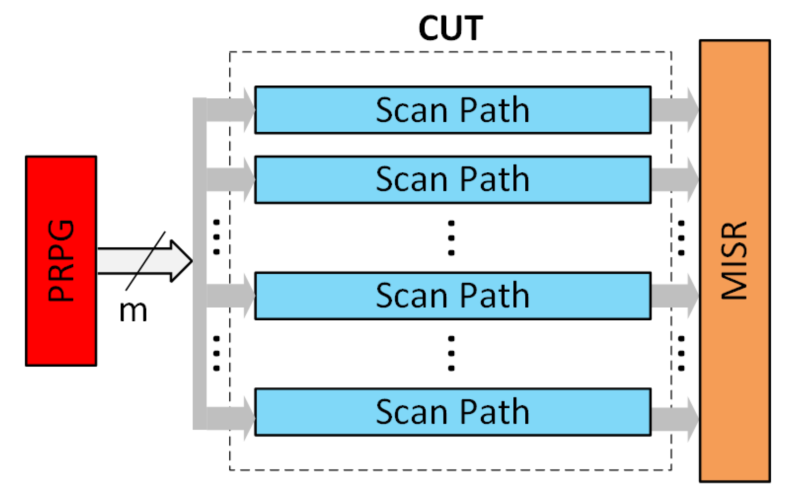
Figure 2.
The example of faults that are undetectable by means of a conventional STUMPS-type LBIST structure.
Figure 2.
The example of faults that are undetectable by means of a conventional STUMPS-type LBIST structure.

Figure 3.
Type I LFSR register associated with the primitive polynomial : (a) Internal structure of the register; (b) State-Time Diagram (STD) for that register.
Figure 3.
Type I LFSR register associated with the primitive polynomial : (a) Internal structure of the register; (b) State-Time Diagram (STD) for that register.

Figure 4.
The graph for the correlation coefficient for an example of the type I LFSR register shown in Figure 3a.
Figure 4.
The graph for the correlation coefficient for an example of the type I LFSR register shown in Figure 3a.

Figure 5.
The graph for the correlation coefficient for an example of the type I LFSR register shown in Figure 3a—the zoomed-in picture for the correlation coefficient ranging from −0.03 to +0.05. The correlation coefficient was calculated for the test sequence with the length of 10,000 vectors.
Figure 5.
The graph for the correlation coefficient for an example of the type I LFSR register shown in Figure 3a—the zoomed-in picture for the correlation coefficient ranging from −0.03 to +0.05. The correlation coefficient was calculated for the test sequence with the length of 10,000 vectors.

Figure 6.
An LBIST module with STUMPS architecture with a pseudo-random test pattern generator composed of the LFSR or CA register and a phase shifter.
Figure 6.
An LBIST module with STUMPS architecture with a pseudo-random test pattern generator composed of the LFSR or CA register and a phase shifter.
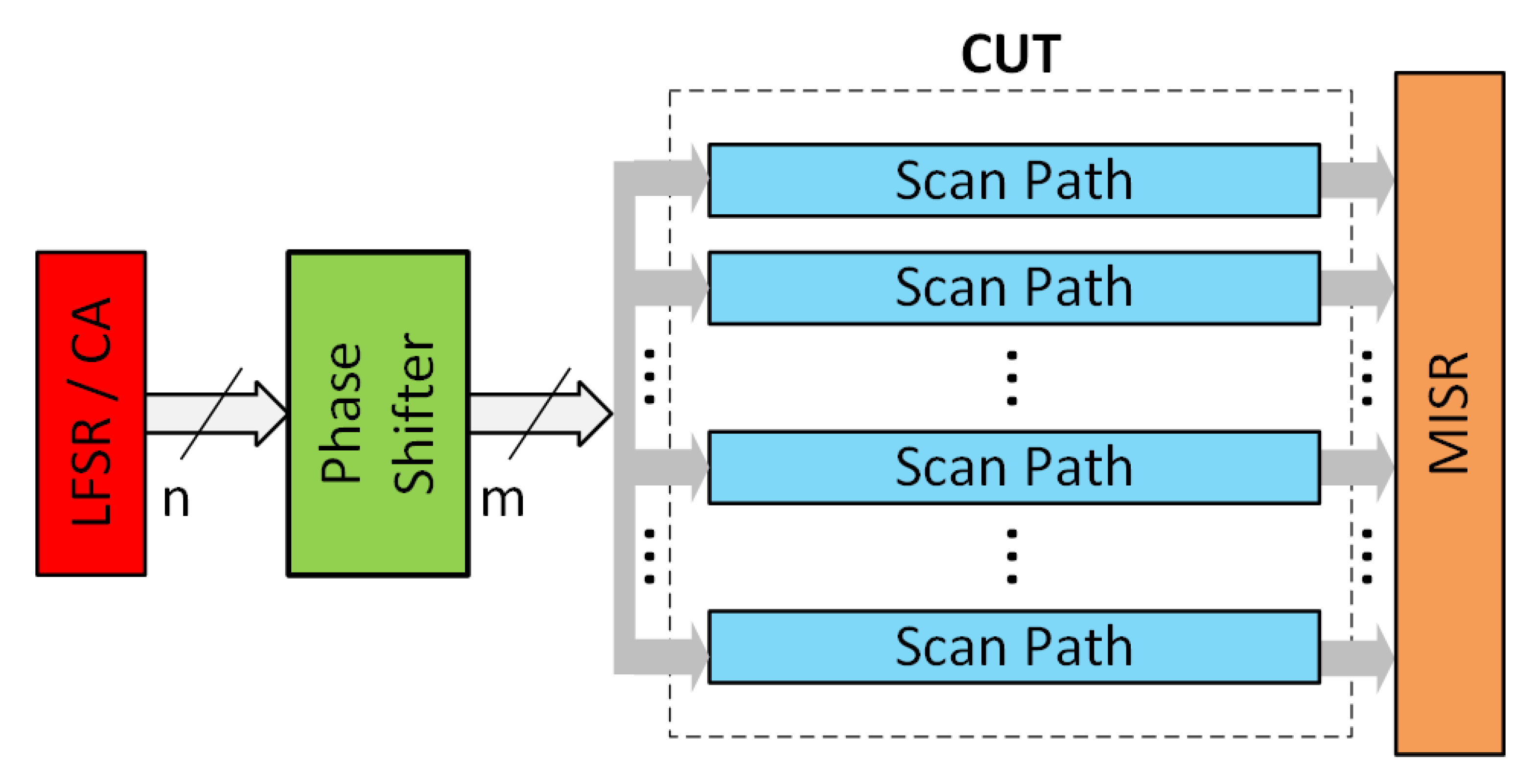
Figure 7.
General structure of an n-bit DT-LFSR register.

Figure 8.
The DT-LFSR register with the D3T17 structure and associated with the primitive polynomial : (a) Internal structure of the register; (b) State–Time Diagram (STD) for that register.
Figure 8.
The DT-LFSR register with the D3T17 structure and associated with the primitive polynomial : (a) Internal structure of the register; (b) State–Time Diagram (STD) for that register.

Figure 9.
The graph for the correlation coefficient for the DT-LFSR with the D3T17 structure.

Figure 10.
The graph for the correlation coefficient for the DT-LFSR with the D3T17 structure—the zoomed-in picture for correlation coefficient range from −0.03 do +0.05, the correlation coefficient was calculated for a test sequence with the length of 10,000 vectors.
Figure 10.
The graph for the correlation coefficient for the DT-LFSR with the D3T17 structure—the zoomed-in picture for correlation coefficient range from −0.03 do +0.05, the correlation coefficient was calculated for a test sequence with the length of 10,000 vectors.

Figure 11.
Explanation of a phase shift in the DT-LFSR register.
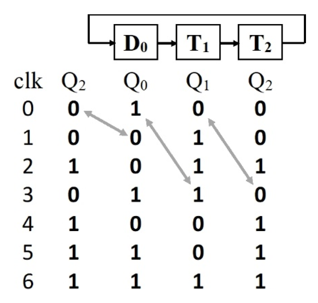
Figure 12.
LBIST module with STUMPS architecture that uses a set of DT-LFSR registers as a generator of pseudo-random test patterns.
Figure 12.
LBIST module with STUMPS architecture that uses a set of DT-LFSR registers as a generator of pseudo-random test patterns.

Figure 13.
n-bit DT-LFSR: (a) Diagram of the internal structure of the synthesizable register model; (b) Internal structure of the configurable D/T flip-flop.
Figure 13.
n-bit DT-LFSR: (a) Diagram of the internal structure of the synthesizable register model; (b) Internal structure of the configurable D/T flip-flop.

Figure 14.
Topology layout for a 20-bit DT-LFSR register with the D3T17 structure and designed by means of the interleaving technique.
Figure 14.
Topology layout for a 20-bit DT-LFSR register with the D3T17 structure and designed by means of the interleaving technique.


Table 1.
Minimum phase shift at outputs of T-type flip-flops within the DT-LFSR register in question.
Table 1.
Minimum phase shift at outputs of T-type flip-flops within the DT-LFSR register in question.
| No. | t | n | Ω | ΦΤ | ΦΤmin |
|---|---|---|---|---|---|
| 1 | 22 | 25 | 3.36 × 10⁷ | 2.29 × 10⁷ | 1.53 × 10⁶ |
| 2 | 25 | 31 | 2.15 × 10⁹ | 1.98 × 10⁹ | 8.59 × 10⁷ |
| 3 | 27 | 29 | 5.37 × 10⁸ | 9.94 × 10⁷ | 1.99 × 10⁷ |
| 4 | 28 | 31 | 2.15 × 10⁹ | 1.30 × 10⁹ | 7.67 × 10⁷ |
| 5 | 33 | 35 | 3.44 × 10¹⁰ | 3.33 × 10¹⁰ | 1.04 × 10⁹ |
| 6 | 38 | 41 | 2.20 × 10¹² | 2.89 × 10¹¹ | 5.79 × 10¹⁰ |
| 7 | 40 | 49 | 5.63 × 10¹⁴ | 5.49 × 10¹⁴ | 1.41 × 10¹³ |
| 8 | 42 | 47 | 1.41 × 10¹⁴ | 3.69 × 10¹³ | 3.35 × 10¹² |
| 9 | 49 | 52 | 4.50 × 10¹⁵ | 2.21 × 10¹⁵ | 9.19 × 10¹³ |
| 10 | 50 | 57 | 1.44 × 10¹⁷ | 4.90 × 10¹⁶ | 2.88 × 10¹⁵ |
| 11 | 58 | 63 | 9.22 × 10¹⁸ | 1.75 × 10¹⁸ | 1.59 × 10¹⁷ |
| 12 | 59 | 60 | 1.15 × 10¹⁸ | 3.91 × 10¹⁷ | 1.95 × 10¹⁶ |
| 13 | 59 | 68 | 2.95 × 10²⁰ | 1.35 × 10²⁰ | 5.00 × 10¹⁸ |
| 14 | 62 | 63 | 9.22 × 10¹⁸ | 1.34 × 10¹⁸ | 1.49 × 10¹⁷ |
| 15 | 62 | 71 | 2.36 × 10²¹ | 3.43 × 10²⁰ | 3.81 × 10¹⁹ |
| 16 | 65 | 71 | 2.36 × 10²¹ | 1.93 × 10²¹ | 3.63 × 10¹⁹ |
| 17 | 65 | 81 | 2.42 × 1024 | 2.08 × 1024 | 3.72 × 10²² |
| 18 | 70 | 79 | 6.04 × 10²³ | 3.20 × 10²³ | 8.64 × 10²¹ |
| 19 | 71 | 84 | 1.93 × 1025 | 5.18 × 1024 | 2.72 × 10²³ |
| 20 | 74 | 87 | 1.55 × 1026 | 1.88 × 1025 | 2.09 × 1024 |
| 21 | 78 | 95 | 3.96 × 1028 | 2.54 × 1027 | 5.08 × 1026 |
| 22 | 84 | 95 | 3.96 × 1028 | 1.93 × 1028 | 4.72 × 1026 |
| 23 | 85 | 97 | 1.58 × 1029 | 2.24 × 1028 | 1.86 × 1027 |
| 24 | 91 | 97 | 1.58 × 1029 | 1.04 × 1028 | 1.74 × 1027 |
Table 2.
The number of scan paths to be fed with test sequences from a TPG designed as a set of DT-LFSR registers, with consideration of various phase shift .
Table 2.
The number of scan paths to be fed with test sequences from a TPG designed as a set of DT-LFSR registers, with consideration of various phase shift .
| No. | t | n | Θmin | |||||
|---|---|---|---|---|---|---|---|---|
| 128 | 256 | 512 | 1024 | 2048 | 4096 | |||
| 1 | 22 | 25 | 11,915 | 5957 | 2978 | 1489 | 744 | 372 |
| 2 | 25 | 31 | 671,088 | 335,544 | 167,772 | 83,886 | 41,943 | 20,971 |
| 3 | 27 | 29 | 155,344 | 77,672 | 38,836 | 19,418 | 9709 | 4854 |
| 4 | 28 | 31 | 599,186 | 299,593 | 149,796 | 74,898 | 37,449 | 18,724 |
| 5 | 33 | 35 | 8,134,407 | 4,067,203 | 2,033,601 | 1,016,800 | 508,400 | 254,200 |
| 6 | 38 | 41 | 4.52 × 10⁸ | 2.26 × 10⁸ | 1.13 × 10⁸ | 5.65 × 10⁷ | 2.83 × 10⁷ | 1.41 × 10⁷ |
| 7 | 40 | 49 | 1.10 × 10¹¹ | 5.50 × 10¹⁰ | 2.75 × 10¹⁰ | 1.37 × 10¹⁰ | 6.87 × 10⁹ | 3.44 × 10⁹ |
| 8 | 42 | 47 | 2.62 × 10¹⁰ | 1.31 × 10¹⁰ | 6.54 × 1009 | 3.27 × 1009 | 1.64 × 10⁹ | 8.18 × 10⁸ |
| 9 | 49 | 52 | 7.18 × 10¹¹ | 3.59 × 10¹¹ | 1.80 × 10¹¹ | 8.98 × 10¹⁰ | 4.49 × 10¹⁰ | 2.24 × 10¹⁰ |
| 10 | 50 | 57 | 2.25 × 10¹³ | 1.13 × 10¹³ | 5.63 × 10¹² | 2.81 × 10¹² | 1.41 × 10¹² | 7.04 × 10¹¹ |
| 11 | 58 | 63 | 1.24 × 10¹⁵ | 6.21 × 10¹⁴ | 3.11 × 10¹⁴ | 1.55 × 10¹⁴ | 7.76 × 10¹³ | 3.88 × 10¹³ |
| 12 | 59 | 60 | 1.53 × 10¹⁴ | 7.63 × 10¹³ | 3.82 × 10¹³ | 1.91 × 10¹³ | 9.54 × 10¹² | 4.77 × 10¹² |
| 13 | 59 | 68 | 3.91 × 10¹⁶ | 1.95 × 10¹⁶ | 9.77 × 10¹⁵ | 4.89 × 10¹⁵ | 2.44 × 10¹⁵ | 1.22 × 10¹⁵ |
| 14 | 62 | 63 | 1.16 × 10¹⁵ | 5.81 × 10¹⁴ | 2.91 × 10¹⁴ | 1.45 × 10¹⁴ | 7.26 × 10¹³ | 3.63 × 10¹³ |
| 15 | 62 | 71 | 2.98 × 10¹⁷ | 1.49 × 10¹⁷ | 7.44 × 10¹⁶ | 3.72 × 10¹⁶ | 1.86 × 10¹⁶ | 9.30 × 10¹⁵ |
| 16 | 65 | 71 | 2.84 × 10¹⁷ | 1.42 × 10¹⁷ | 7.09 × 10¹⁶ | 3.55 × 10¹⁶ | 1.77 × 10¹⁶ | 8.87 × 10¹⁵ |
| 17 | 65 | 81 | 2.91 × 10²⁰ | 1.45 × 10²⁰ | 7.27 × 10¹⁹ | 3.63 × 10¹⁹ | 1.82 × 10¹⁹ | 9.08 × 10¹⁸ |
| 18 | 70 | 79 | 6.75 × 10¹⁹ | 3.37 × 10¹⁹ | 1.69 × 10¹⁹ | 8.43 × 10¹⁸ | 4.22 × 10¹⁸ | 2.11 × 10¹⁸ |
| 19 | 71 | 84 | 2.13 × 10²¹ | 1.06 × 10²¹ | 5.32 × 10²⁰ | 2.66 × 10²⁰ | 1.33 × 10²⁰ | 6.65 × 10¹⁹ |
| 20 | 74 | 87 | 1.63 × 10²² | 8.17 × 10²¹ | 4.08 × 10²¹ | 2.04 × 10²¹ | 1.02 × 10²¹ | 5.11 × 10²⁰ |
| 21 | 78 | 95 | 3.97 × 1024 | 1.98 × 1024 | 9.92 × 10²³ | 4.96 × 10²³ | 2.48 × 10²³ | 1.24 × 10²³ |
| 22 | 84 | 95 | 3.68 × 1024 | 1.84 × 1024 | 9.21 × 10²³ | 4.61 × 10²³ | 2.30 × 10²³ | 1.15 × 10²³ |
| 23 | 85 | 97 | 1.46 × 1025 | 7.28 × 1024 | 3.64 × 1024 | 1.82 × 1024 | 9.10 × 10²³ | 4.55 × 10²³ |
| 24 | 91 | 97 | 1.36 × 1025 | 6.80 × 1024 | 3.40 × 1024 | 1.70 × 1024 | 8.50 × 10²³ | 4.25 × 10²³ |
Table 3.
The maximum numbers of scan paths to be fed from LFSR + PS or from CA + PS structures for various phase shifts .
Table 3.
The maximum numbers of scan paths to be fed from LFSR + PS or from CA + PS structures for various phase shifts .
| PRPG Type | n | Θmin | |||||
|---|---|---|---|---|---|---|---|
| 128 | 256 | 512 | 1024 | 2048 | 4096 | ||
| LFSR I [34] | 24 | 2019 | 1989 | 1938 | 1827 | 1630 | 1362 |
| 32 | 4991 | 4991 | 4990 | 4987 | 4982 | 4971 | |
| LFSR II [34] | 24 | 3437 | 3346 | 3194 | 2920 | 2454 | 1908 |
| 32 | 13,477 | 13,473 | 13,465 | 13,442 | 13,395 | 13,309 | |
| LHCA 90/150 [39] | 24 | 10,858 | 10,031 | 8713 | 6902 | 4863 | 3063 |
| 32 | 39,731 | 39,677 | 39,584 | 39,398 | 39,018 | 38,301 | |
Table 4.
Maximum numbers of output channels for test pattern generators of the DT-LFSR-TPG type when the separation between output channels is high.
Table 4.
Maximum numbers of output channels for test pattern generators of the DT-LFSR-TPG type when the separation between output channels is high.
| No. | t | n | Θmin | ||||||||
|---|---|---|---|---|---|---|---|---|---|---|---|
| 105 | 106 | 107 | 108 | 109 | 1010 | 1011 | 1012 | 1013 | |||
| 1 | 22 | 25 | 15 | 1 | - | - | - | - | - | - | - |
| 2 | 25 | 31 | 858 | 85 | 8 | - | - | - | - | - | - |
| 3 | 27 | 29 | 198 | 19 | 1 | - | - | - | - | - | - |
| 4 | 28 | 31 | 766 | 76 | 7 | - | - | - | - | - | - |
| 5 | 33 | 35 | 10,412 | 1041 | 104 | 10 | 1 | - | - | - | - |
| 6 | 38 | 41 | 578,690 | 57,869 | 5786 | 578 | 57 | 5 | - | - | - |
| 7 | 40 | 49 | 1.41 × 10⁸ | 14,073,748 | 1,407,374 | 140,737 | 14,073 | 1407 | 140 | 14 | 1 |
| 8 | 42 | 47 | 33,508,925 | 3,350,892 | 335,089 | 33,508 | 3350 | 335 | 33 | 3 | - |
| 9 | 49 | 52 | 9.19 × 10⁸ | 91,910,196 | 9,191,019 | 919,101 | 91,910 | 9191 | 919 | 91 | 9 |
| 10 | 50 | 57 | 2.88 × 10¹⁰ | 2.88 × 10⁹ | 2.88 × 10⁸ | 28,823,037 | 2,882,303 | 288,230 | 28,823 | 2882 | 288 |
| 11 | 58 | 63 | 1.59 × 10¹² | 1.59 × 10¹¹ | 1.59 × 10¹⁰ | 1.59 × 10⁹ | 1.59 × 10⁸ | 15,902,365 | 1,590,236 | 159,023 | 15,902 |
| 12 | 59 | 60 | 1.95 × 10¹¹ | 1.95 × 10¹⁰ | 1.95 × 10⁹ | 1.95 × 10⁸ | 19,541,042 | 1,954,104 | 195,410 | 19,541 | 1954 |
| 13 | 59 | 68 | 5.00 × 10¹³ | 5.00 × 10¹² | 5.00 × 10¹¹ | 5.00 × 10¹⁰ | 5.00 × 10⁹ | 5.00 × 10⁸ | 50,025,068 | 5,002,506 | 500,250 |
| 14 | 62 | 63 | 1.49 × 10¹² | 1.49 × 10¹¹ | 1.49 × 10¹⁰ | 1.49 × 10⁹ | 1.49 × 10⁸ | 14,876,406 | 1,487,640 | 148,764 | 14,876 |
| 15 | 62 | 71 | 3.81 × 10¹⁴ | 3.81 × 10¹³ | 3.81 × 10¹² | 3.81 × 10¹¹ | 3.81 × 10¹⁰ | 3.81 × 10⁹ | 3.81 × 10⁸ | 38,083,600 | 3,808,360 |
| 16 | 65 | 71 | 3.63 × 10¹⁴ | 3.63 × 10¹³ | 3.63 × 10¹² | 3.63 × 10¹¹ | 3.63 × 10¹⁰ | 3.63 × 10⁹ | 3.63 × 10⁸ | 36,325,896 | 3,632,589 |
| 17 | 65 | 81 | 3.72 × 10¹⁷ | 3.72 × 10¹⁶ | 3.72 × 10¹⁵ | 3.72 × 10¹⁴ | 3.72 × 10¹³ | 3.72 × 10¹² | 3.72 × 10¹¹ | 3.72 × 10¹⁰ | 3.72 × 10⁹ |
| 18 | 70 | 79 | 8.64 × 10¹⁶ | 8.64 × 10¹⁵ | 8.64 × 10¹⁴ | 8.64 × 10¹³ | 8.64 × 10¹² | 8.64 × 10¹¹ | 8.64 × 10¹⁰ | 8.64 × 10⁹ | 8.64 × 10⁸ |
| 19 | 71 | 84 | 2.72 × 10¹⁸ | 2.72 × 10¹⁷ | 2.72 × 10¹⁶ | 2.72 × 10¹⁵ | 2.72 × 10¹⁴ | 2.72 × 10¹³ | 2.72 × 10¹² | 2.72 × 10¹¹ | 2.72 × 10¹⁰ |
| 20 | 74 | 87 | 2.09 × 10¹⁹ | 2.09 × 10¹⁸ | 2.09 × 10¹⁷ | 2.09 × 10¹⁶ | 2.09 × 10¹⁵ | 2.09 × 10¹⁴ | 2.09 × 10¹³ | 2.09 × 10¹² | 2.09 × 10¹¹ |
| 21 | 78 | 95 | 5.08 × 10²¹ | 5.08 × 10²⁰ | 5.08 × 10¹⁹ | 5.08 × 10¹⁸ | 5.08 × 10¹⁷ | 5.08 × 10¹⁶ | 5.08 × 10¹⁵ | 5.08 × 10¹⁴ | 5.08 × 10¹³ |
| 22 | 84 | 95 | 4.72 × 10²¹ | 4.72 × 10²⁰ | 4.72 × 10¹⁹ | 4.72 × 10¹⁸ | 4.72 × 10¹⁷ | 4.72 × 10¹⁶ | 4.72 × 10¹⁵ | 4.72 × 10¹⁴ | 4.72 × 10¹³ |
| 23 | 85 | 97 | 1.86 × 10²² | 1.86 × 10²¹ | 1.86 × 10²⁰ | 1.86 × 10¹⁹ | 1.86 × 10¹⁸ | 1.86 × 10¹⁷ | 1.86 × 10¹⁶ | 1.86 × 10¹⁵ | 1.86 × 10¹⁴ |
| 24 | 91 | 97 | 1.74 × 10²² | 1.74 × 10²¹ | 1.74 × 10²⁰ | 1.74 × 10¹⁹ | 1.74 × 10¹⁸ | 1.74 × 10¹⁷ | 1.74 × 10¹⁶ | 1.74 × 10¹⁵ | 1.74 × 10¹⁴ |
Table 5.
Minimum phase shift Ψmin between binary sequences produced by a TPG designed on the basis of DT-LFSR registers, calculated for various numbers of scan paths.
Table 5.
Minimum phase shift Ψmin between binary sequences produced by a TPG designed on the basis of DT-LFSR registers, calculated for various numbers of scan paths.
| No. | t | n | Number of Scan Paths | ||||||
|---|---|---|---|---|---|---|---|---|---|
| 128 | 256 | 512 | 1024 | 2048 | 4096 | 8192 | |||
| 1 | 22 | 25 | 1.19 × 10⁴ | 5.96 × 10³ | 2.98 × 10³ | 1.49 × 10³ | 7.44 × 10² | 3.72 × 10² | 1.86 × 10² |
| 2 | 25 | 31 | 6.71 × 10⁵ | 3.36 × 10⁵ | 1.68 × 10⁵ | 8.39 × 10⁴ | 4.19 × 10⁴ | 2.10 × 10⁴ | 1.05 × 10⁴ |
| 3 | 27 | 29 | 1.55 × 10⁵ | 7.77 × 10⁴ | 3.88 × 10⁴ | 1.94 × 10⁴ | 9.71 × 10³ | 4.85 × 10³ | 2.43 × 10³ |
| 4 | 28 | 31 | 5.99 × 10⁵ | 3.00 × 10⁵ | 1.50 × 10⁵ | 7.49 × 10⁴ | 3.74 × 10⁴ | 1.87 × 10⁴ | 9.36 × 10³ |
| 5 | 33 | 35 | 8.13 × 10⁶ | 4.07 × 10⁶ | 2.03 × 10⁶ | 1.02 × 10⁶ | 5.08 × 10⁵ | 2.54 × 10⁵ | 1.27 × 10⁵ |
| 6 | 38 | 41 | 4.52 × 10⁸ | 2.26 × 10⁸ | 1.13 × 10⁸ | 5.65 × 10⁷ | 2.83 × 10⁷ | 1.41 × 10⁷ | 7.06 × 10⁶ |
| 7 | 40 | 49 | 1.10 × 10¹¹ | 5.50 × 10¹⁰ | 2.75 × 10¹⁰ | 1.37 × 10¹⁰ | 6.87 × 10⁹ | 3.44 × 10⁹ | 1.72 × 10⁹ |
| 8 | 42 | 47 | 2.62 × 10¹⁰ | 1.31 × 10¹⁰ | 6.54 × 10⁹ | 3.27 × 10⁹ | 1.64 × 10⁹ | 8.18 × 10⁸ | 4.09 × 10⁸ |
| 9 | 49 | 52 | 7.18 × 10¹¹ | 3.59 × 10¹¹ | 1.80 × 10¹¹ | 8.98 × 10¹⁰ | 4.49 × 10¹⁰ | 2.24 × 10¹⁰ | 1.12 × 10¹⁰ |
| 10 | 50 | 57 | 2.25 × 10¹³ | 1.13 × 10¹³ | 5.63 × 10¹² | 2.81 × 10¹² | 1.41 × 10¹² | 7.04 × 10¹¹ | 3.52 × 10¹¹ |
| 11 | 58 | 63 | 1.24 × 10¹⁵ | 6.21 × 10¹⁴ | 3.11 × 10¹⁴ | 1.55 × 10¹⁴ | 7.76 × 10¹³ | 3.88 × 10¹³ | 1.94 × 10¹³ |
| 12 | 59 | 60 | 1.53 × 10¹⁴ | 7.63 × 10¹³ | 3.82 × 10¹³ | 1.91 × 10¹³ | 9.54 × 10¹² | 4.77 × 10¹² | 2.39 × 10¹² |
| 13 | 59 | 68 | 3.91 × 10¹⁶ | 1.95 × 10¹⁶ | 9.77 × 10¹⁵ | 4.89 × 10¹⁵ | 2.44 × 10¹⁵ | 1.22 × 10¹⁵ | 6.11 × 10¹⁴ |
| 14 | 62 | 63 | 1.16 × 10¹⁵ | 5.81 × 10¹⁴ | 2.91 × 10¹⁴ | 1.45 × 10¹⁴ | 7.26 × 10¹³ | 3.63 × 10¹³ | 1.82 × 10¹³ |
| 15 | 62 | 71 | 2.98 × 10¹⁷ | 1.49 × 10¹⁷ | 7.44 × 10¹⁶ | 3.72 × 10¹⁶ | 1.86 × 10¹⁶ | 9.30 × 10¹⁵ | 4.65 × 10¹⁵ |
| 16 | 65 | 71 | 2.84 × 10¹⁷ | 1.42 × 10¹⁷ | 7.09 × 10¹⁶ | 3.55 × 10¹⁶ | 1.77 × 10¹⁶ | 8.87 × 10¹⁵ | 4.43 × 10¹⁵ |
| 17 | 65 | 81 | 2.91 × 10²⁰ | 1.45 × 10²⁰ | 7.27 × 10¹⁹ | 3.63 × 10¹⁹ | 1.82 × 10¹⁹ | 9.08 × 10¹⁸ | 4.54 × 10¹⁸ |
| 18 | 70 | 79 | 6.75 × 10¹⁹ | 3.37 × 10¹⁹ | 1.69 × 10¹⁹ | 8.43 × 10¹⁸ | 4.22 × 10¹⁸ | 2.11 × 10¹⁸ | 1.05 × 10¹⁸ |
| 19 | 71 | 84 | 2.13 × 10²¹ | 1.06 × 10²¹ | 5.32 × 10²⁰ | 2.66 × 10²⁰ | 1.33 × 10²⁰ | 6.65 × 10¹⁹ | 3.33 × 10¹⁹ |
| 20 | 74 | 87 | 1.63 × 10²² | 8.17 × 10²¹ | 4.08 × 10²¹ | 2.04 × 10²¹ | 1.02 × 10²¹ | 5.11 × 10²⁰ | 2.55 × 10²⁰ |
| 21 | 78 | 95 | 3.97 × 1024 | 1.98 × 1024 | 9.92 × 10²³ | 4.96 × 10²³ | 2.48 × 10²³ | 1.24 × 10²³ | 6.20 × 10²² |
| 22 | 84 | 95 | 3.68 × 1024 | 1.84 × 1024 | 9.21 × 10²³ | 4.61 × 10²³ | 2.30 × 10²³ | 1.15 × 10²³ | 5.76 × 10²² |
| 23 | 85 | 97 | 1.46 × 1025 | 7.28 × 1024 | 3.64 × 1024 | 1.82 × 1024 | 9.10 × 10²³ | 4.55 × 10²³ | 2.28 × 10²³ |
| 24 | 91 | 97 | 1.36 × 1025 | 6.80 × 1024 | 3.40 × 1024 | 1.70 × 1024 | 8.50 × 10²³ | 4.25 × 10²³ | 2.13 × 10²³ |
Table 6.
Results of the logic synthesis for selected registers of the DT-LFSR type.
| No. | t | n | Total Cost | Cost Per Channel |
|---|---|---|---|---|
| 1 | 22 | 25 | 176 | 8.00 |
| 2 | 25 | 31 | 212 | 8.48 |
| 3 | 27 | 29 | 209 | 7.74 |
| 4 | 28 | 31 | 220 | 7.86 |
| 5 | 33 | 35 | 253 | 7.67 |
| 6 | 38 | 41 | 294 | 7.74 |
| 7 | 40 | 49 | 335 | 8.38 |
| 8 | 42 | 47 | 332 | 7.90 |
| 9 | 49 | 52 | 374 | 7.63 |
| 10 | 50 | 57 | 400 | 8.00 |
| 11 | 58 | 63 | 449 | 7.74 |
| 12 | 59 | 60 | 439 | 7.44 |
| 13 | 59 | 68 | 474 | 8.03 |
| 14 | 62 | 63 | 461 | 7.44 |
| 15 | 62 | 71 | 496 | 8.00 |
| 16 | 65 | 71 | 505 | 7.77 |
| 17 | 65 | 81 | 549 | 8.45 |
| 18 | 70 | 79 | 555 | 7.93 |
| 19 | 71 | 84 | 580 | 8.17 |
| 20 | 74 | 87 | 602 | 8.14 |
| 21 | 78 | 95 | 649 | 8.32 |
| 22 | 84 | 95 | 667 | 7.94 |
| 23 | 85 | 97 | 678 | 7.98 |
| 24 | 91 | 97 | 696 | 7.65 |
Table 7.
Implementation costs for test pattern generators of the DT-LFSR-TPG type.
| No. | t | n | Number of Scan Paths | |||||
|---|---|---|---|---|---|---|---|---|
| 128 | 256 | 512 | 1024 | 2048 | 4096 | |||
| 1 | 22 | 25 | 1056 | 2112 | 4224 | 8272 | 16,544 | 32,912 |
| 2 | 25 | 31 | 1272 | 2332 | 4452 | 8692 | 17,384 | 34,768 |
| 3 | 27 | 29 | 1045 | 2090 | 3971 | 7942 | 15,884 | 31,768 |
| 4 | 28 | 31 | 1100 | 2200 | 4180 | 8140 | 16,280 | 32,340 |
| 5 | 33 | 35 | 1012 | 2024 | 4048 | 8096 | 15,939 | 31,625 |
| 6 | 38 | 41 | 1176 | 2058 | 4116 | 7938 | 15,876 | 31,752 |
| 7 | 40 | 49 | 1340 | 2345 | 4355 | 8710 | 17,420 | 34,505 |
| 8 | 42 | 47 | 1328 | 2324 | 4316 | 8300 | 16,268 | 32,536 |
| 9 | 49 | 52 | 1122 | 2244 | 4114 | 7854 | 15,708 | 31,416 |
| 10 | 50 | 57 | 1200 | 2400 | 4400 | 8400 | 16,400 | 32,800 |
| 11 | 58 | 63 | 1347 | 2245 | 4041 | 8082 | 16,164 | 31,879 |
| 12 | 59 | 60 | 1317 | 2195 | 3951 | 7902 | 15,365 | 30,730 |
| 13 | 59 | 68 | 1422 | 2370 | 4266 | 8532 | 16,590 | 33,180 |
| 14 | 62 | 63 | 1383 | 2305 | 4149 | 7837 | 15,674 | 30,887 |
| 15 | 62 | 71 | 1488 | 2480 | 4464 | 8432 | 16,864 | 33,232 |
| 16 | 65 | 71 | 1010 | 2020 | 4040 | 8080 | 16,160 | 32,320 |
| 17 | 65 | 81 | 1098 | 2196 | 4392 | 8784 | 17,568 | 35,136 |
| 18 | 70 | 79 | 1110 | 2220 | 4440 | 8325 | 16,650 | 32,745 |
| 19 | 71 | 84 | 1160 | 2320 | 4640 | 8700 | 16,820 | 33,640 |
| 20 | 74 | 87 | 1204 | 2408 | 4214 | 8428 | 16,856 | 33,712 |
| 21 | 78 | 95 | 1298 | 2596 | 4543 | 9086 | 17,523 | 34,397 |
| 22 | 84 | 95 | 1334 | 2668 | 4669 | 8671 | 16,675 | 32,683 |
| 23 | 85 | 97 | 1356 | 2712 | 4746 | 8814 | 16,950 | 33,222 |
| 24 | 91 | 97 | 1392 | 2088 | 4176 | 8352 | 16,008 | 32,016 |
Table 8.
Supplementary details on the structures of test pattern generators of the DT-LFSR-TPG type.
Table 8.
Supplementary details on the structures of test pattern generators of the DT-LFSR-TPG type.
| No. | t | n | Number of Scan Paths | |||||
|---|---|---|---|---|---|---|---|---|
| 128 | 256 | 512 | 1024 | 2048 | 4096 | |||
| 1 | 22 | 25 | 6, 18, 4 | 12, 36, 8 | 24, 72, 16 | 47, 141, 10 | 94, 282, 20 | 187, 561, 18 |
| 2 | 25 | 31 | 6, 36, 22 | 11, 66, 19 | 21, 126, 13 | 41, 246, 1 | 82, 492, 2 | 164, 984, 4 |
| 3 | 27 | 29 | 5, 10, 7 | 10, 20, 14 | 19, 38, 1 | 38, 76, 2 | 76, 152, 4 | 152, 304, 8 |
| 4 | 28 | 31 | 5, 15, 12 | 10, 30, 24 | 19, 57, 20 | 37, 111, 12 | 74, 222, 24 | 147, 441, 20 |
| 5 | 33 | 35 | 4, 8, 4 | 8, 16, 8 | 16, 32, 16 | 32, 64, 32 | 63, 126, 31 | 125, 250, 29 |
| 6 | 38 | 41 | 4, 12, 24 | 7, 21, 10 | 14, 42, 20 | 27, 81, 2 | 54, 162, 4 | 108, 324, 8 |
| 7 | 40 | 49 | 4, 36, 32 | 7, 63, 24 | 13, 117, 8 | 26, 234, 16 | 52, 468, 32 | 103, 927, 24 |
| 8 | 42 | 47 | 4, 20, 40 | 7, 35, 38 | 13, 65, 34 | 25, 125, 26 | 49, 245, 10 | 98, 490, 20 |
| 9 | 49 | 52 | 3, 9, 19 | 6, 18, 38 | 11, 33, 27 | 21, 63, 5 | 42, 126, 10 | 84, 252, 20 |
| 10 | 50 | 57 | 3, 21, 22 | 6, 42, 44 | 11, 77, 38 | 21, 147, 26 | 41, 287, 2 | 82, 574, 4 |
| 11 | 58 | 63 | 3, 15, 46 | 5, 25, 34 | 9, 45, 10 | 18, 90, 20 | 36, 180, 40 | 71, 355, 22 |
| 12 | 59 | 60 | 3, 3, 49 | 5, 5, 39 | 9, 9, 19 | 18, 18, 38 | 35, 35, 17 | 70, 70, 34 |
| 13 | 59 | 68 | 3, 27, 49 | 5, 45, 39 | 9, 81, 19 | 18, 162, 38 | 35, 315, 17 | 70, 630, 34 |
| 14 | 62 | 63 | 3, 3, 58 | 5, 5, 54 | 9, 9, 46 | 17, 17, 30 | 34, 34, 60 | 67, 67, 58 |
| 15 | 62 | 71 | 3, 27, 58 | 5, 45, 54 | 9, 81, 46 | 17, 153, 30 | 34, 306, 60 | 67, 603, 58 |
| 16 | 65 | 71 | 2, 12, 2 | 4, 24, 4 | 8, 48, 8 | 16, 96, 16 | 32, 192, 32 | 64, 384, 64 |
| 17 | 65 | 81 | 2, 32, 2 | 4, 64, 4 | 8, 128, 8 | 16, 256, 16 | 32, 512, 32 | 64, 1024, 64 |
| 18 | 70 | 79 | 2, 18, 12 | 4, 36, 24 | 8, 72, 48 | 15, 135, 26 | 30, 270, 52 | 59, 531, 34 |
| 19 | 71 | 84 | 2, 26, 14 | 4, 52, 28 | 8, 104, 56 | 15, 195, 41 | 29, 377, 11 | 58, 754, 22 |
| 20 | 74 | 87 | 2, 26, 20 | 4, 52, 40 | 7, 91, 6 | 14, 182, 12 | 28, 364, 24 | 56, 728, 48 |
| 21 | 78 | 95 | 2, 34, 28 | 4, 68, 56 | 7, 119, 34 | 14, 238, 68 | 27, 459, 58 | 53, 901, 38 |
| 22 | 84 | 95 | 2, 22, 40 | 4, 44, 80 | 7, 77, 76 | 13, 143, 68 | 25, 275, 52 | 49, 539, 20 |
| 23 | 85 | 97 | 2, 24, 42 | 4, 48, 84 | 7, 84, 83 | 13, 156, 81 | 25, 300, 77 | 49, 588, 69 |
| 24 | 91 | 97 | 2, 12, 54 | 3, 18, 17 | 6, 36, 34 | 12, 72, 68 | 23, 138, 45 | 46, 276, 90 |
Table 9.
Implementation costs and maximum operation frequencies for test pattern generators of the LFSR + PS type disclosed in [34].
Table 9.
Implementation costs and maximum operation frequencies for test pattern generators of the LFSR + PS type disclosed in [34].
| Number of Scan Paths | Type I LFSRs | Type II LFSRs | ||||||||||
|---|---|---|---|---|---|---|---|---|---|---|---|---|
| h1(x) | h2(x) | h3(x) | h4(x) | h5(x) | h6(x) | h1(x) | h2(x) | h3(x) | h4(x) | h5(x) | h6(x) | |
| 128 | 459 | 527 | 603 | 667 | 725 | 862 | 461 | 525 | 588 | 656 | 717 | 864 |
| 575 | 614 | 614 * | 614 * | 614 * | 614 * | 567 | 668 | 711 | 831 | 665 | 796 | |
| 256 | 794 | 839 | 940 | 964 | 1061 | 1148 | 785 | 837 | 919 | 975 | 1054 | 1150 |
| 563 | 516 | 614 * | 582 | 588 | 515 | 584 | 536 | 659 | 642 | 641 | 697 | |
| 512 | 1306 | 1456 | 1523 | 1568 | 1650 | 1823 | 1308 | 1454 | 1508 | 1570 | 1648 | 1804 |
| 435 | 521 | 511 | 473 | 499 | 565 | 448 | 551 | 543 | 486 | 514 | 586 | |
| 1024 | 2542 | 2553 | 2650 | 2759 | 2824 | 2969 | 2430 | 2550 | 2649 | 2753 | 2822 | 2958 |
| 424 | 425 | 425 | 510 | 474 | 492 | 437 | 431 | 433 | 523 | 485 | 501 | |
| 2048 | 5008 | 4950 | 4982 | 5028 | 5131 | 5218 | 4995 | 4946 | 4980 | 5027 | 5131 | 5214 |
| 356 | 419 | 416 | 408 | 439 | 368 | 373 | 431 | 434 | 410 | 450 | 392 | |
| 4096 | 9738 | 10046 | 9622 | 9697 | 9775 | 9905 | 9641 | 10026 | 9618 | 9663 | 9757 | 9877 |
| 342 | 352 | 375 | 417 | 415 | 418 | 342 | 368 | 398 | 440 | 421 | 436 | |
Table 10.
Comparison of implementation costs and maximum operating frequencies between test pattern generators of the LFSR + PS and DT-LFSR-TPG types.
Table 10.
Comparison of implementation costs and maximum operating frequencies between test pattern generators of the LFSR + PS and DT-LFSR-TPG types.
| Number of Scan Paths | Type I LFSRs | Type II LFSRs | ||||||||||
|---|---|---|---|---|---|---|---|---|---|---|---|---|
| h1(x) | h2(x) | h3(x) | h4(x) | h5(x) | h6(x) | h1(x) | h2(x) | h3(x) | h4(x) | h5(x) | h6(x) | |
| 128 | 120% | 91% | 68% | 51% | 39% | 17% | 119% | 92% | 72% | 54% | 41% | 17% |
| 73% | 62% | 62% | 62% | 62% | 62% | 75% | 49% | 40% | 20% | 50% | 25% | |
| 256 | 154% | 141% | 115% | 110% | 90% | 76% | 157% | 141% | 120% | 107% | 92% | 76% |
| 76% | 93% | 62% | 71% | 69% | 93% | 70% | 86% | 51% | 55% | 55% | 43% | |
| 512 | 203% | 171% | 159% | 152% | 139% | 117% | 202% | 172% | 162% | 152% | 140% | 119% |
| 129% | 91% | 95% | 110% | 99% | 76% | 122% | 80% | 83% | 104% | 93% | 70% | |
| 1024 | 208% | 207% | 196% | 184% | 178% | 164% | 223% | 207% | 196% | 185% | 178% | 165% |
| 134% | 134% | 134% | 95% | 110% | 102% | 128% | 130% | 129% | 90% | 105% | 98% | |
| 2048 | 207% | 210% | 208% | 206% | 199% | 194% | 208% | 211% | 209% | 206% | 199% | 195% |
| 180% | 137% | 139% | 144% | 126% | 170% | 167% | 131% | 129% | 142% | 121% | 154% | |
| 4096 | 216% | 206% | 219% | 217% | 214% | 210% | 219% | 207% | 220% | 218% | 215% | 211% |
| 191% | 183% | 165% | 139% | 140% | 138% | 190% | 170% | 150% | 126% | 136% | 128% | |
Publisher’s Note: MDPI stays neutral with regard to jurisdictional claims in published maps and institutional affiliations. |
© 2021 by the author. Licensee MDPI, Basel, Switzerland. This article is an open access article distributed under the terms and conditions of the Creative Commons Attribution (CC BY) license (https://creativecommons.org/licenses/by/4.0/).
Share and Cite
MDPI and ACS Style
Garbolino, T. A New, Fast Pseudo-Random Pattern Generator for Advanced Logic Built-In Self-Test Structures. Appl. Sci. 2021, 11, 9476. https://doi.org/10.3390/app11209476
AMA Style
Garbolino T. A New, Fast Pseudo-Random Pattern Generator for Advanced Logic Built-In Self-Test Structures. Applied Sciences. 2021; 11(20):9476. https://doi.org/10.3390/app11209476
Chicago/Turabian StyleGarbolino, Tomasz. 2021. "A New, Fast Pseudo-Random Pattern Generator for Advanced Logic Built-In Self-Test Structures" Applied Sciences 11, no. 20: 9476. https://doi.org/10.3390/app11209476
Note that from the first issue of 2016, this journal uses article numbers instead of page numbers. See further details here.