Abstract
A new hybrid DC converter is proposed and implemented to have wide voltage variation operation and bidirectional power flow capability for photovoltaic power applications. The hybrid DC converter, including a half- or full-bridge resonant circuit, is adopted to realize the bidirectional power operation and low switching losses. To overcome the wide voltage variation problem (60 V–480 V) from photovoltaic panels due to sunlight intensity, the full-bridge structure or half-bridge structure resonant circuit is used in the presented converter to implement high or low voltage gain under a low or high input voltage condition. Using a pulse frequency modulation (PFM) scheme, the voltage transfer function of the resonant circuit is controlled to regulate the load voltage. Due to the symmetric circuit structures used on the primary and the secondary sides in the proposed converter, the bidirectional power flow can be achieved with the same circuit characteristics. Therefore, the proposed converter can be applied to battery stacks to achieve charger and discharger operations. Finally, a 400 W prototype is implemented, and the performance of the proposed hybrid DC converter is confirmed by the experiments.
1. Introduction
Bidirectional DC converters [1,2,3,4,5,6] have been proposed to interface between the different DC voltage buses for renewable energy sources, battery chargers/dischargers, uninterrupted power supplies, and electric vehicles. For electric vehicle applications [7,8], bidirectional power factor correctors and bidirectional DC converters have been proposed to realize grid-to-vehicle and vehicle-to-grid operations. Phase-shift pulse-width modulation (PWM) converters have been proposed in [9,10] to realize a forward power flow operation with a voltage step-down operation, and achieve reverse power flow with a voltage step-up operation. The main drawbacks of phase-shift PWM converters are a high freewheeling current and hard switching loss at light load conditions. Dual active bridge (DAB) converters have been studied and proposed in [11,12,13,14] to realize bidirectional power flow using a phase-shift PWM technique and duty cycle control. However, two control variables, the phase-shift angle and duty cycle, are more difficult to be calculated and derived compared to the other bidirectional DC converters. Symmetric CLLC converters have been proposed in [15,16] to accomplish forward and reverse power flow operations for DC distribution systems and battery charging/discharging systems. The primary-side and secondary-side have the same circuit structures in CLLC converters. Therefore, the forward and backward voltage transfer functions are identical and the circuit characteristics for both power flows are identical. The power switches can be turned on at soft switching operation due to the circuit characteristics of the resonant converter with frequency modulation. The main drawback of the CLLC converter is a narrow voltage operation range due to its low voltage gain. Therefore, the CLLC converter cannot work well under wide voltage variation conditions, such as solar power applications. To realize wide voltage variation capability, cascade DC converters have been proposed in [17,18], with a buck or boost circuit on the front-stage and a PWM converter on the rear stage. The main problem of cascade DC converters is high conduction loss. PWM converters or resonant converters with serial–parallel circuit structures have been studied in [19,20,21,22] to realize wide input voltage operation (Vin,max/Vin,min < 4). However, only forward power flow can be realized in these circuit topologies.
According to the foregoing studies, a DC hybrid symmetric resonant converter for battery charging and discharging is proposed in this paper. One AC switch and one hybrid half/full-bridge circuit structure are used on both the primary-side and secondary-side to achieve wide voltage input operation and bidirectional power flow operation. The benefits of the proposed converter are as follows: (1) wide voltage operation from 60 V–480 V input; (2) symmetric circuit on both the primary and secondary sides to have the same voltage transfer function for backward and reverse power operations; and (3) soft switching operation on power semiconductors due to resonant circuit characteristics with frequency modulation. The proposed converter can be applied to photovoltaic power applications or battery charging/discharging systems. A 400 W prototype is provided to verify the proposed bidirectional power flow converter. The experimental results demonstrated that the maximum circuit efficiency of the prototype is approximately 93.6%. The circuit diagram of the proposed hybrid DC converter is discussed in Section 2. In Section 3, the principle operations of the converter are provided. The circuit characteristics and a design example are described in Section 4. Experimental results are provided and discussed in Section 5, to verify the feasibility of the theoretical discussions. The conclusions of the proposed circuit are described in Section 6.
2. Circuit Diagram of the Proposed Hybrid DC Converter
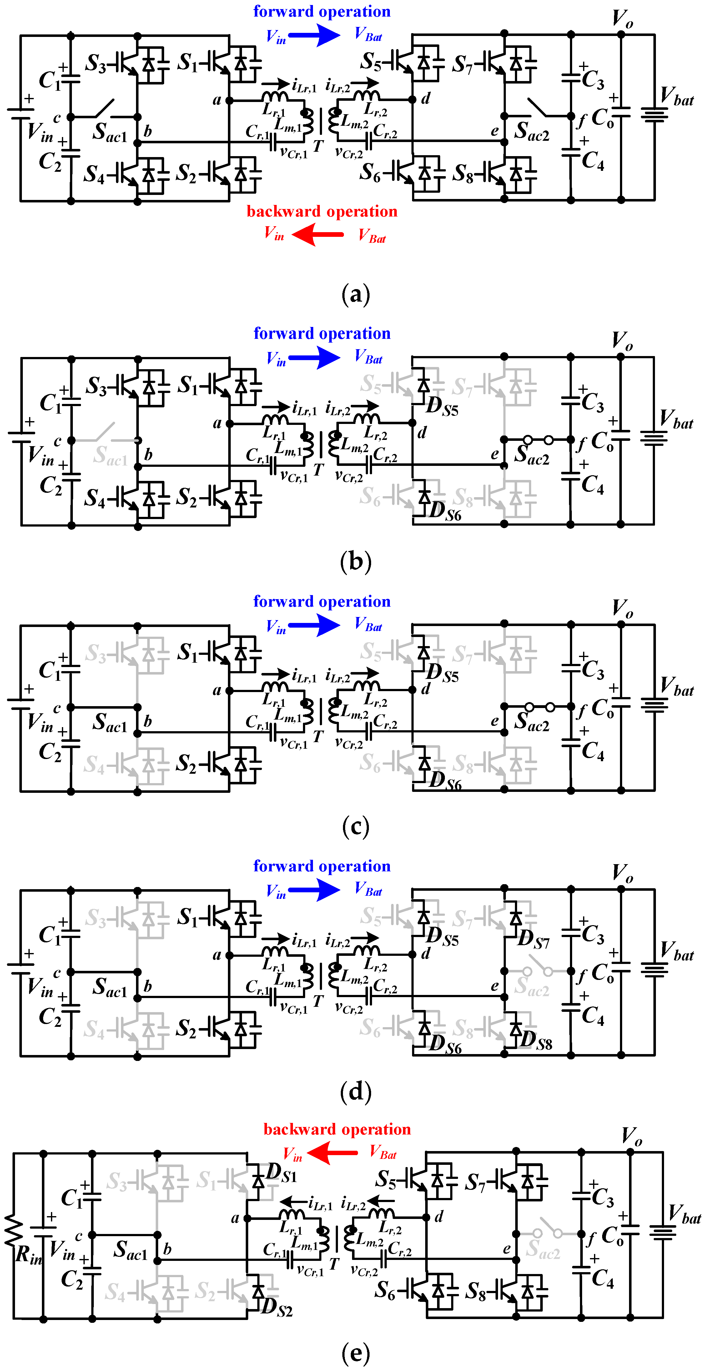
Figure 1a gives the circuit diagram of a hybrid DC converter. The primary and secondary sides of the isolated transformer have the same circuit structure. Full-power switches and one AC switch are used on each side. The AC switches Sac1 and Sac2 are implemented by two switches connected back-to-back. On each side, the resonant circuit can be operated at the full-bridge structure (S1–S4) or half-bridge structure (S1, S2, and Sac1), related to low or high input voltage range conditions. For forward power flow operation, S5–S8 are all inactive. Therefore, the right-hand side circuit operates as a half-wave (Sac2 is on) or full-wave (Sac2 is off) diode rectifier. The proposed hybrid converter has three operation modes to achieve wide input voltage variation. In each operation mode, the circuit can achieve two times the input voltage range. Therefore, the wide input voltage range variation Vin,max = 8Vin,min (where Vin,min = 60 V and Vin,max = 480 V) can be implemented in the proposed converter. When Vin,min ≤ Vin < 2Vin,min, the high voltage gain is needed in the proposed converter. Therefore, the full-bridge resonant circuit (Sac1 is off) is operated on the left-hand side and the half-wave diode rectifier (or voltage doubler rectifier) (Sac2 is on) is operated on the right-hand side, as shown in Figure 1b, to achieve the maximum voltage gain. When 2Vin,min ≤ Vin < 4Vin,min, the half-bridge resonant circuit (Sac1 is on and S3 and S4 are off) is used on the left-hand side and half-wave diode rectifier (Sac2 is on) is selected on the right-hand side (Figure 1c) to obtain medium voltage gain. If 4Vin,min ≤ Vin < 8Vin,min, the half-bridge resonant circuit (Sac1 is on and S3 and S4 are off) and full-wave diode rectifier (Sac2 is off) are selected on the left-hand side and right-hand side, respectively (Figure 1d), to obtain the minimum voltage gain. For backward power flow operation (Figure 1e), S1–S4 are off and Sac1 is on. Thus, the left-hand side circuit operates as a half-wave diode rectifier. S5–S8 are controlled with the PFM scheme to deliver power from the Vo terminal to the Vin terminal.
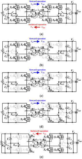
Figure 1.
Presented hybrid DC converter: (a) circuit structure; (b) low voltage range input under forward power flow; (c) medium voltage range input under forward power flow; (d) high voltage range input under forward power flow; (e) under baclward power flow operation.
3. Operation Principle
Two main advantages of the proposed converter are wide voltage variation operation and bidirectional power flow operation. Under forward power flow operation, three operations modes, shown in Figure 1b–d, can be operated according to the low, medium and high voltage range inputs. Under backward power flow operation (Figure 1e), power switches on the secondary side are controlled to reverse the power flow from the load side to the input side.
3.1. Low Voltage Range Input (Vin,min ≤ Vin < 2Vin,min) under Forward Power Flow
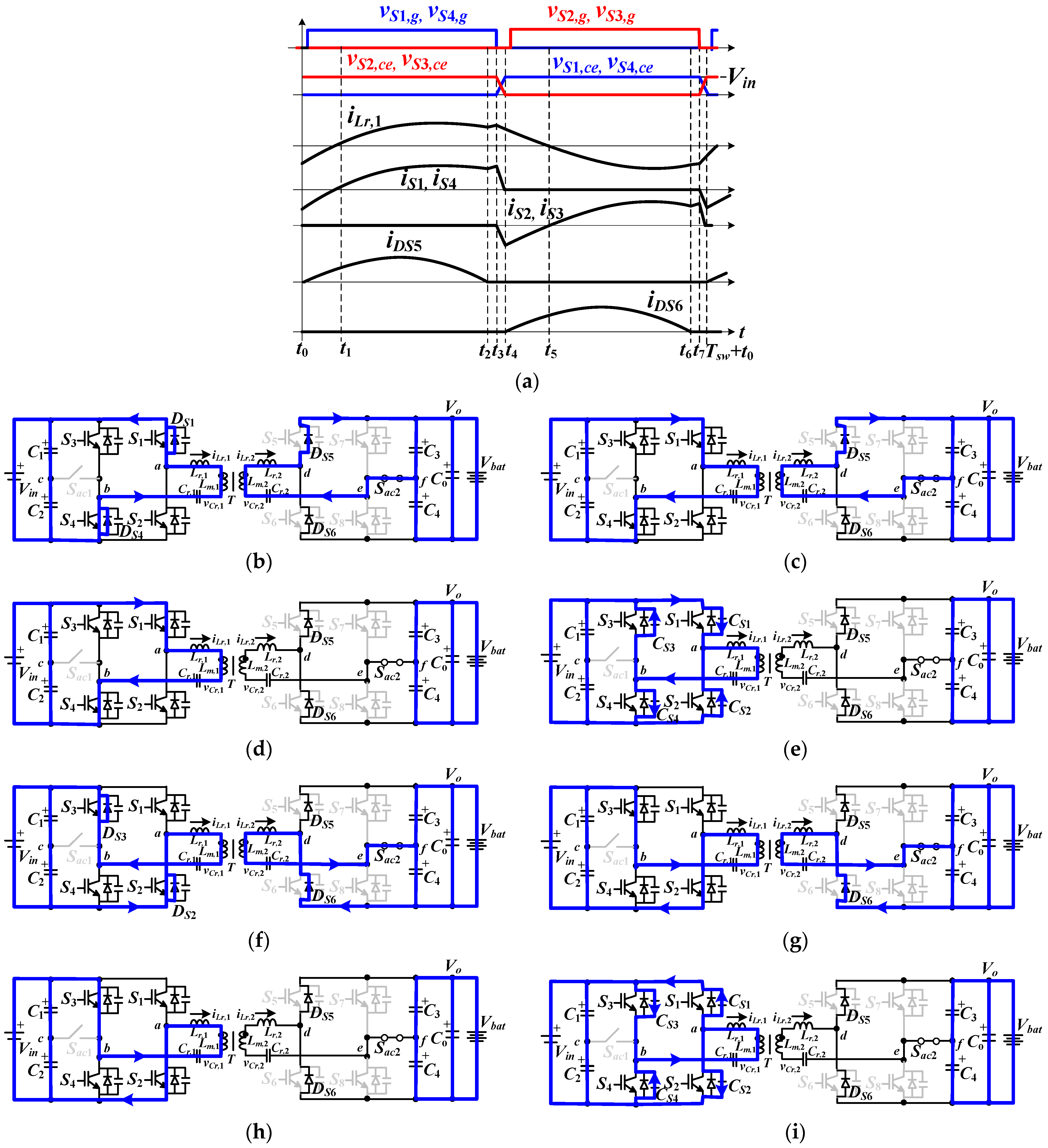
If the input voltage is in the low voltage range, the full-bridge resonant circuit is used on the primary side and the half-wave diode rectifier is adopted on the secondary side to achieve the maximum voltage gain. Therefore, Sac1 and S5–S8 are off and Sac2 is on, as shown in Figure 1b. From the pulse-width modulation signals of S1–S4, DS5, and DS6, one can observe that there are eight switching states (Figure 2a) in every switching cycle if fsw (switching frequency) < fr (resonant frequency). The circuit components are assumed as Cr,2 = n2Cr,1 and Lr,2 = Lr,1/n2, where n = np/ns, to simplify the circuit analysis. Therefore, the series resonant frequency on the primary and secondary sides are identical, . The state circuit operations related to the eight switching states are provided in Figure 2b–i.
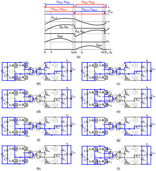
Figure 2.
PWM signals and state circuits under low voltage range input and forward power flow: (a) PWM signals; (b) State 1; (c) State 2; (d) State 3; (e) State 4; (f) State 5; (g) State 6; (h) State 7; (i) State 8.
State 1 [t0 ≤ t < t1]: When t = t0, vS1,ce = vS4,ce = 0. iLr,1(t0) < 0 will flow through diodes DS1 and DS4. Then, S1 and S4 can turn on at zero-voltage switching. The secondary side current iLr,2 flows through diode DS5 to charge capacitor C3. In this state, iLr,1 increases from a negative value to zero ampere.
State 2 [t1 ≤ t < t2]: When t > t1, iLr,1 becomes a positive value. Then iLr,1 flows through S1 and S4. Forward power flow is from Vin to Vo in State 2 operation. The converter leg voltages are Vab = Vin and Vde = VC3 = Vo/2. The resonant frequency in State 2 is given as .
State 3 [t2 ≤ t < t3]: When fsw is less than fr,1, iLr,2 will be decreased to zero at time t2. The rectifier diode DS5 becomes off. In State 3, the resonant frequency of iLr,1 is . No power is transferred to output load in this state.
State 4 [t3 ≤ t < t4]: When t = t3, S1 and S4 are turned off. iLr,1 discharges CS2 and CS3 where CS2 and CS3 are the output capacitors of S2 and S3, respectively. If the primary current , where CS,p = CS1 = CS2 = CS3 = CS4 (CS1–CS3 are output capacitors of S1–S4, respectively) and is the peak value of iLm,1, then CS2 and CS3 can be discharged to zero voltage at time t4.
State 5 [t4 ≤ t < t5]: The capacitor voltages vCS2 = vCS3 = 0 (or vS2,ce = vS3,ce = 0) at time t4. Then iLr,1(t4) > 0 will flow through DS2 and DS3. The zero-voltage turn-on operation of S2 and S3 can be implemented after time t4. The secondary side current iLr,2 will be decreased and DS6 becomes forward biased. The primary curent iLr,1 is decreased and capacitor C4 is charged in State 5.
State 6 [t5 ≤ t < t6]: After t > t5, iLr,1 < 0. Then, DS2 and DS3 become reverse biased. iLr,1 will flow through S2 and S3. In State 6, iLr,1 is decreased and C4 is charged by iLr,2. The resonant frequency is .
State 7 [t6 ≤ t < t7]: At t = t6, the secondary side current iLr,2 = 0 and DS6 becomes reverse biased. The resonant frequency in this state is .
State 8 [t7 ≤ t < Tsw + t0]: When t = t7, S2 and S3 turn off. iLr,1(t7) < 0 will discharge CS1 and CS4. The one switching period ends at time Tsw + t0.
3.2. Medium Voltage Range Input (2Vin,min ≤ Vin < 4Vin,min) under Forward Power Flow
When a medium voltage range is input to the proposed converter, the half-bridge resonant circuit is operated on the left-hand side (Figure 1c). Since the input voltage of the resonant circuit is ±Vin/2 instead of ±Vin in Figure 1b, the voltage gain in Figure 1c is only 1/2 of the voltage gain in Figure 1b. One can observe in Figure 1c that Sac1 is on and S3 and S4 are off. Only S1 and S2 are operated with the PFM scheme. Sac2 is on and the half-wave diode rectifier or voltage doubler rectifier is operated on the secondary side. Since the half-bridge resonant circuit (Figure 1c) and full-bridge resonant circuit (Figure 1b) have similar operation states, the circuit operations of the proposed converter under a medium voltage range input are neglected in this subsection.
3.3. High Voltage Range Input (4Vin,min ≤ Vin < 8Vin,min) under Forward Power Flow
When the input voltage is in the high voltage range, the half-bridge resonant circuit is operated on the left-hand side and the full-wave diode rectifier (Sac2 is off) is operated on the right-hand side, as shown in Figure 1d. Comparing Figure 1c,d, the leg voltage vde is ±Vo in Figure 1d instead of ±Vo/2 in Figure 1c with voltage doubler rectifier structure. Therefore, the converter in the Figure 1d operation has less voltage gain than the Figure 1c operation. From Figure 1b–d, it can be concluded that the Figure 1b circuit is selected to control the load voltage with the maximum voltage gain under a low voltage range input condition, and the Figure 1d circuit is selected to regulate the load voltage with the minimum voltage gain under high voltage range input conditions. The circuit operation in Figure 1d is similar to the circuit operation in Figure 1b,c. Thus, the operation principle of the Figure 1d circuit is neglected in this subsection.
3.4. Backward Power Flow
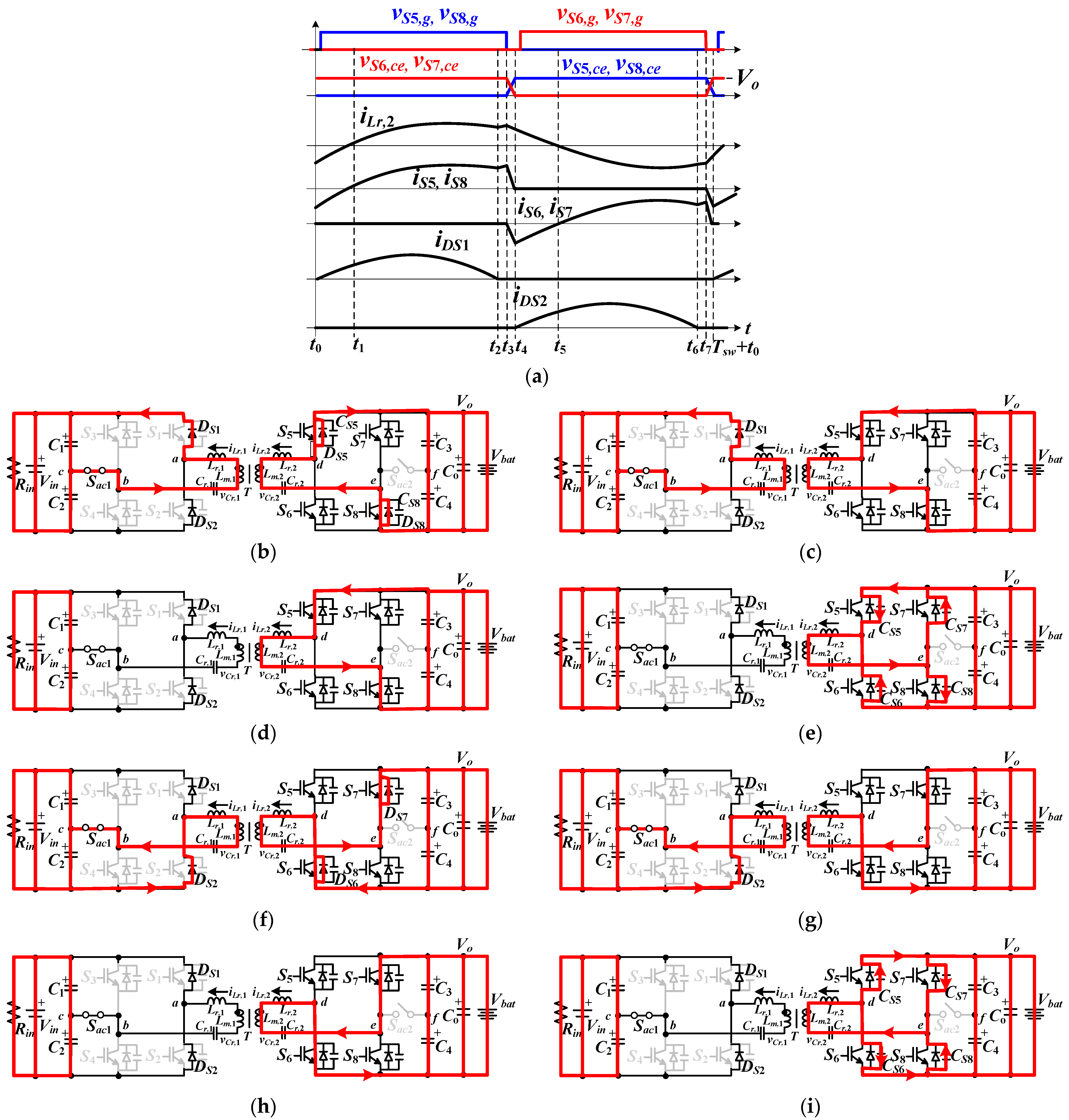
If the converter is operated at backward power operation, the power flow is transferred from Vo to Vin, as shown in Figure 1e. Since Vin is controlled at 400 V, the half-wave diode rectifier is used on the left-hand side. Therefore, Sac1 is on. The full-bridge resonant circuit is operated on the right-hand side so that Sac2 is off and S5–S8 are operated with the PFM scheme. Figure 3a provides the switching signals of the converter under backward power flow in every switching cycle. Figure 3b–i show these state equivalent circuits.
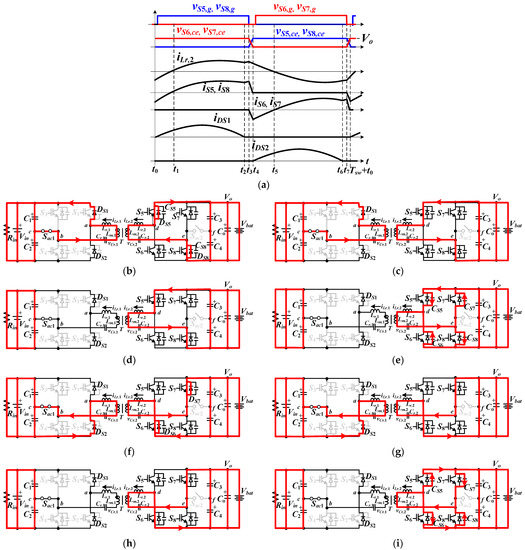
Figure 3.
PWM signals and state circuits under backward power flow: (a) PWM signals; (b) State 1; (c) State 2; (d) State 3; (e) State 4; (f) State 5; (g) State 6; (h) State 7; (i) State 8.
State 1 [t0 ≤ t < t1]: CS5 and CS8 are discharged to zero voltage at t0. iLr,2(t0) is negative so that DS5 anf DS8 are forward biased. Active switches S5 and S8 can be turned on after t0 to have soft switching turn-on operation. Since iLr,1 > 0, DS1 is forward biased and C1 is charged.
State 2 [t1 ≤ t < t2]: At t1, iLr,2 > 0. Thus, iLr2 flows through S5 and S8. Backward power is transferred from Vo to Vin in this state. One can obtain Vab = VC1 = Vin/2 and Vde = Vo. The resonant frequency is .
State 3 [t2 ≤ t < t3]: If fsw < fr,1, iLr,1 = 0 at t2 and DS1 is reverse biased. The resonant frequency on right-hand side circuit is and fp,2 < fp,1.
State 4 [t3 ≤ t < t4]: S5 and S8 are off at t3. Due to iLr,2(t3) > 0, CS6 and CS7 are discharged by iLr,2.
State 5 [t4 ≤ t < t5]: CS6 and CS7 are discharged to zero voltage at t4. Since iLr,2(t4) > 0, iLr,2 flows through DS6 anf DS7. Then, S6 and S7 turn on after t4 to achieve soft switching turn-on operation. Owing to iLr,1 < 0, DS2 becomes forward biased and C2 is charged.
State 6 [t5 ≤ t < t6]: After t5, iLr,2 < 0 and iLr,2 flows through S6 and S7. Backward power flow is from Vo to Vin in this state operation.
State 7 [t6 ≤ t < t7]: iLr,1 = 0 at t6. Then, DS2 is off. The resonant frequency on the right-hand side circuit is .
State 8 [t7 ≤ t < Tsw + t0]: S6 and S7 turn off at t7. Since iLr,2(t7) < 0, iLr,2 discharges CS5 and CS8. At time Tsw + t0, CS5 and CS8 are discharged to zero voltage.
4. Circuit Characteristics and Design Example
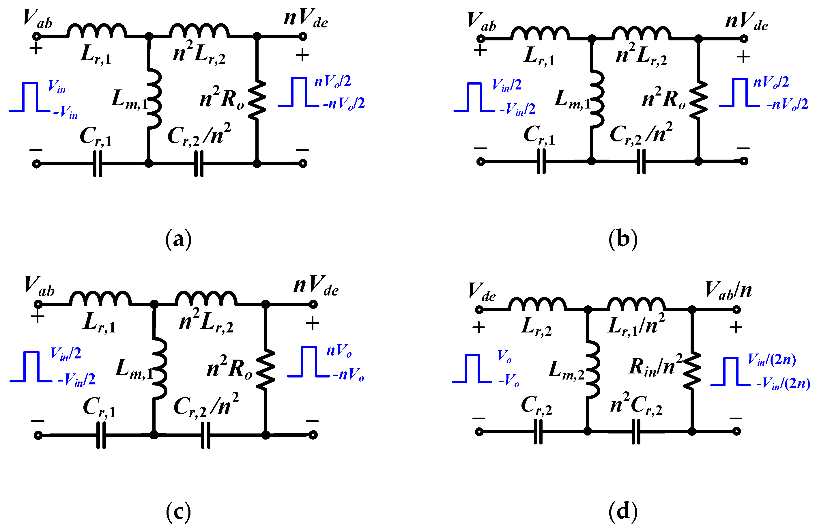
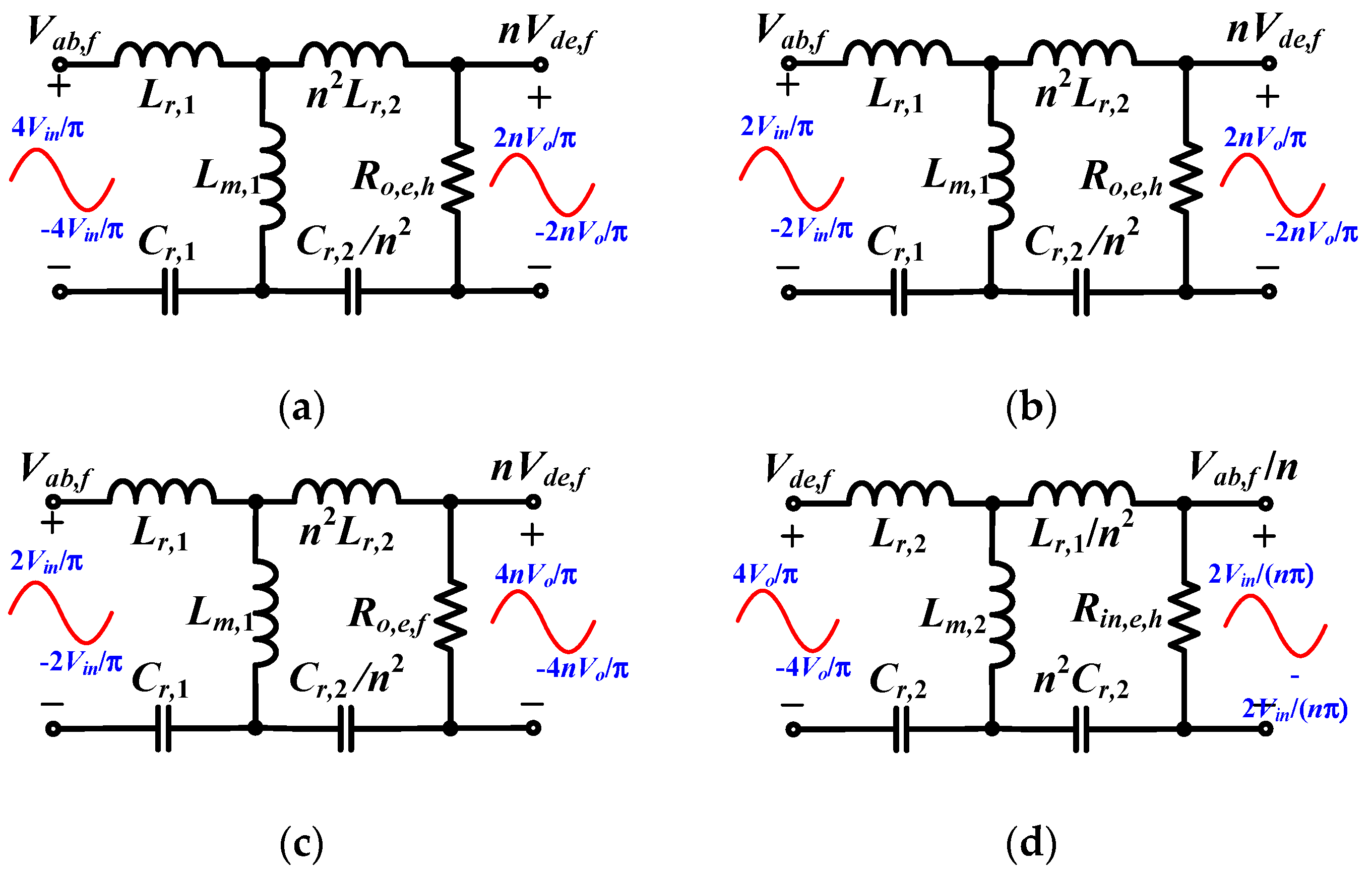
There are four operating modes in the proposed circuit, as shown in Figure 1. In each mode, the PFM scheme is selected to control the active switches so that the voltage gain of the resonant circuit is depended on the switching frequency. The equivalent resonant circuits in Figure 1b–e can be redrawn and is shown in Figure 4. For the forward power flow operation, the leg voltage Vab is a square-wave voltage with ± Vin (low voltage range input condition) or ± Vin/2 (medium and high voltage range input conditions). The leg voltage Vde on the right-hand side of the converter is a square-wave voltage with ± Vo/2 (low and medium voltage range input conditions) or ±Vo (high voltage range input condition). For the backward power flow operation, the leg voltages Vab = ± Vin/2 and Vde = ± Vo. According to the Fourier Series Analysis, the square-wave voltage can be expressed as the summation of the fundamental sinewave voltage and the higher-order harmonic components. Since the higher-order harmonic components are less than the fundamental frequency voltage, only the fundamental sinewave voltage is adopted in the following consideration. The analysis of fundamental frequency is used in [23] to analyze the resonant converter and simplify the circuit analysis. Figure 5 provides the resonant circuits with the fundamental frequency analysis method under four operating modes. If the leg voltage Vab = ± Vin/2 (Figure 4b–d) or ± Vin (Figure 4a), then its fundamental root-mean-square (rms) voltage can be obtained as (Figure 5b–d) or (Figure 5a). Similarly, the rms voltage (Figure 5a,b) or (Figure 5c,d) if Vde = ± Vo/2 (Figure 4a,b) or ± Vo (Figure 4c,d). In Figure 5, Ro,e,h and Ro,e,f are the fundamental load resistances under the half-wave diode rectifier (Figure 5a,b) and full-wave diode rectifier (Figure 5c) operation with forward power flow operation.
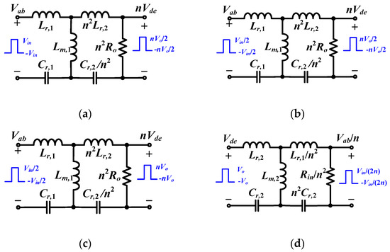
Figure 4.
Equivalent resonant circuits under four operating modes: (a) low voltage range input with forward power flow; (b) medium voltage range input with forward power flow; (c) high voltage range input with forward power flow; (d) backward power flow operation.
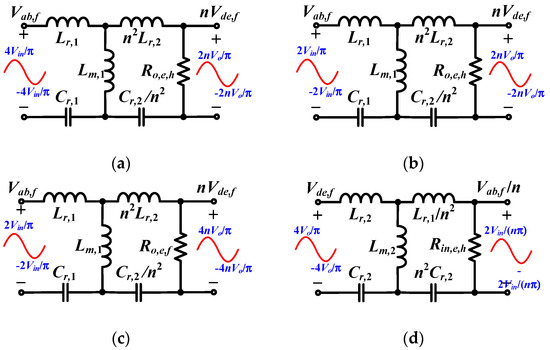
Figure 5.
Resonant circuits using fundamental frequency analysis: (a) low voltage range input with forward power flow; (b) medium voltage range input with forward power flow; (c) high voltage range input with forward power flow; (d) backward power flow operation.
Similarly, the fundamental load resistance Rin,e,h (Figure 5d) under backward power flow operation is given in Equation (3).
The voltage transfer functions in Figure 5a–d are derived in Equations (4)–(7), where Mac,F,L, Mac,F,M, and Mac,F,H are the voltage transfer functions at the low, medium, and high voltage range inputs under forward power flow operation and Mac,B is the voltage transfer function under backward power flow operation.
The following parameters are defined: , ,, , , and . The voltage gains in the four operation modes in (4)–(7) can be expressed in (8)–(10) for the low, medium, and high voltage range inputs under forward power flow and in (11) for backward power flow operation.
It is clear that Equations (8)–(11) have a similar voltage transfer function but different DC voltage gain.
In the following sub-section, a design example of the hybrid DC converter is discussed and presented. For forward power flow, the input and output electric parameters are Vin = 60 V–480 V, Vo = 40 V–52 V, Io,max = 7.7 A, and fr,1 = 100 kHz. For the backward power flow operation, the electric parameters are Vo = 42 V–48 V, Vin = 400 V, Pin,max = 400 W, and fr,2 = 100 kHz. The constant current/constant voltage is adopted to charge the battery under forward power flow operation. If 60 V ≤ Vin < 120 V (low voltage range), then the full-bridge resonant circuit is operated on the left-hand side and the half-wave diode rectifier is used on the right-hand side of the converter, as shown in Figure 1b. If 120 V ≤ Vin < 240 V (medium voltage range), then the half-bridge resonant circuit is operated on the left-hand side and half-wave diode rectifier is used on the right-hand side of the converter, as shown in Figure 1c. If 240 V ≤ Vin ≤ 480 V (high voltage range), then the half-bridge resonant circuit and full-wave diode rectifier are is operated on the left-hand side and right-hand side of the converter, respectively, as shown in Figure 1d. Due to the gains of the four mode operations in (8)–(11) having a similar transfer function, the circuit parameters in the laboratory prototype are obtained from low voltage range input (Vin = 60 V–120 V) under forward power flow. In the prototype design, the minimum voltage gain |Mac,F,L|min is set at unity under Vin = 120 V and Vo = 40 V. The turn-ratio n of T is obtained from Equation (8) and given in Equation (12).
The transformer T is implemented by magnetic core PC40/EE55 with 22 turns on the primary side and 4 turns on the secondary side. Thus, the actual turn-ratio n = 22/4 = 5.5. The maximum and minimum voltage gains at low voltage range input conditions are given in (13) and (14).
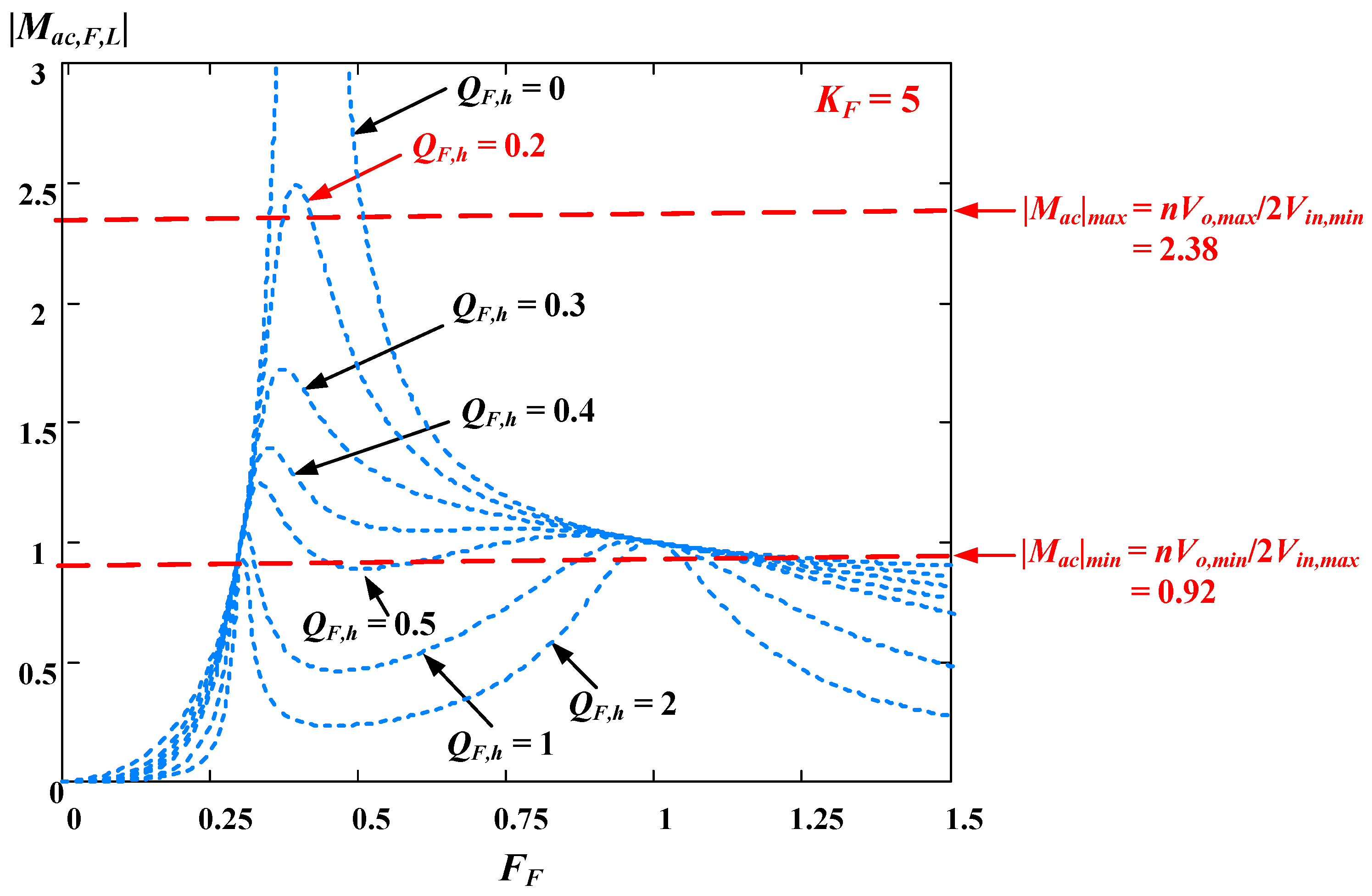
The gain curves of the transfer function at the low voltage range input condition under KF = 5 are plotted in Figure 6. Since the maximum voltage gain at Vin = 60 V and Vo = 52 V is 2.38 in (13), the quality factor QF,h = 0.2 is selected to have a peak voltage gain (= 2.5), which is greater than |Gac,F,L|max = 2.38. Therefore, the switching frequency index FF is created and obtained under Vin = 60 V–120 V and Vo = 40 V–52 V. Then, the equivalent resistance Ro,e,h at full load is obtained as

Figure 6.
Gain curves of the converter at low voltage range input.
The resonant components on the primary-side of the converter are calculated in Equations (16) and (17).
Since KF = 5, the magnetizing inductance Lm,1 = KFLr,1 = 65 µH. The resonant components on the secondary-side of the converter are Lr,2 = Lr,1/n2 ≈ 0.43 µH and Cr,2 = n2Cr,1 ≈ 5.8 µF. Magnetic cores PC40/EER35 are used to implement Lr,1 and Lr,2. S1–S4 and Sac1 are implemented by power switches FGH60N60 with a 600 V/60 A rating. S5–S8 and Sac2 are implemented by power switches P80NF12 with a 120 V/80 A rating. The capacitances are C1 = C2 = 560 μF/400 V, C3 = C4 = 220 μF/100 V, and Co = 660 μF/100 V. Table 1 gives the circuit parameters used in the prototype circuit.

Table 1.
Circuit parameters used in the prototype circuit.
5. Experimental Results
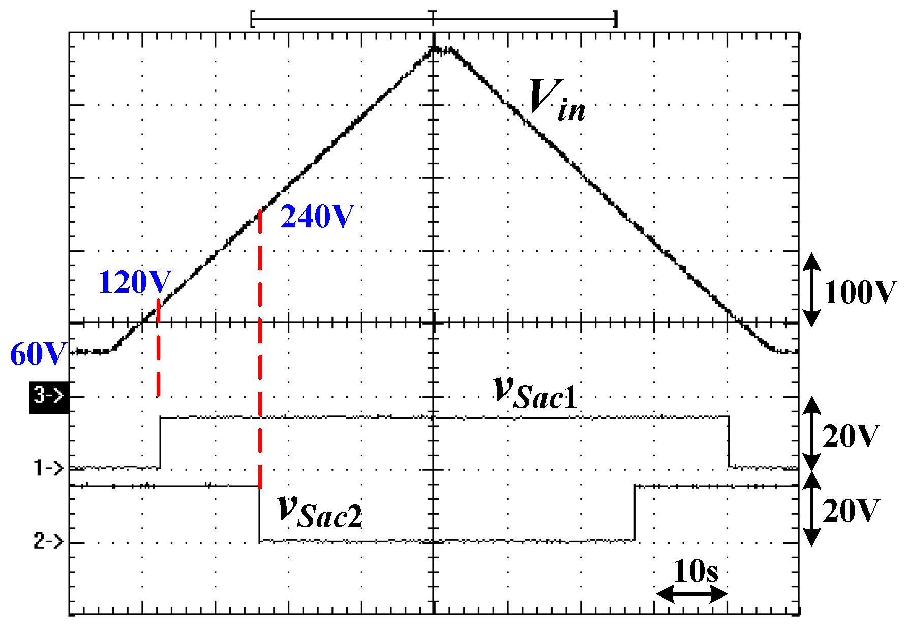
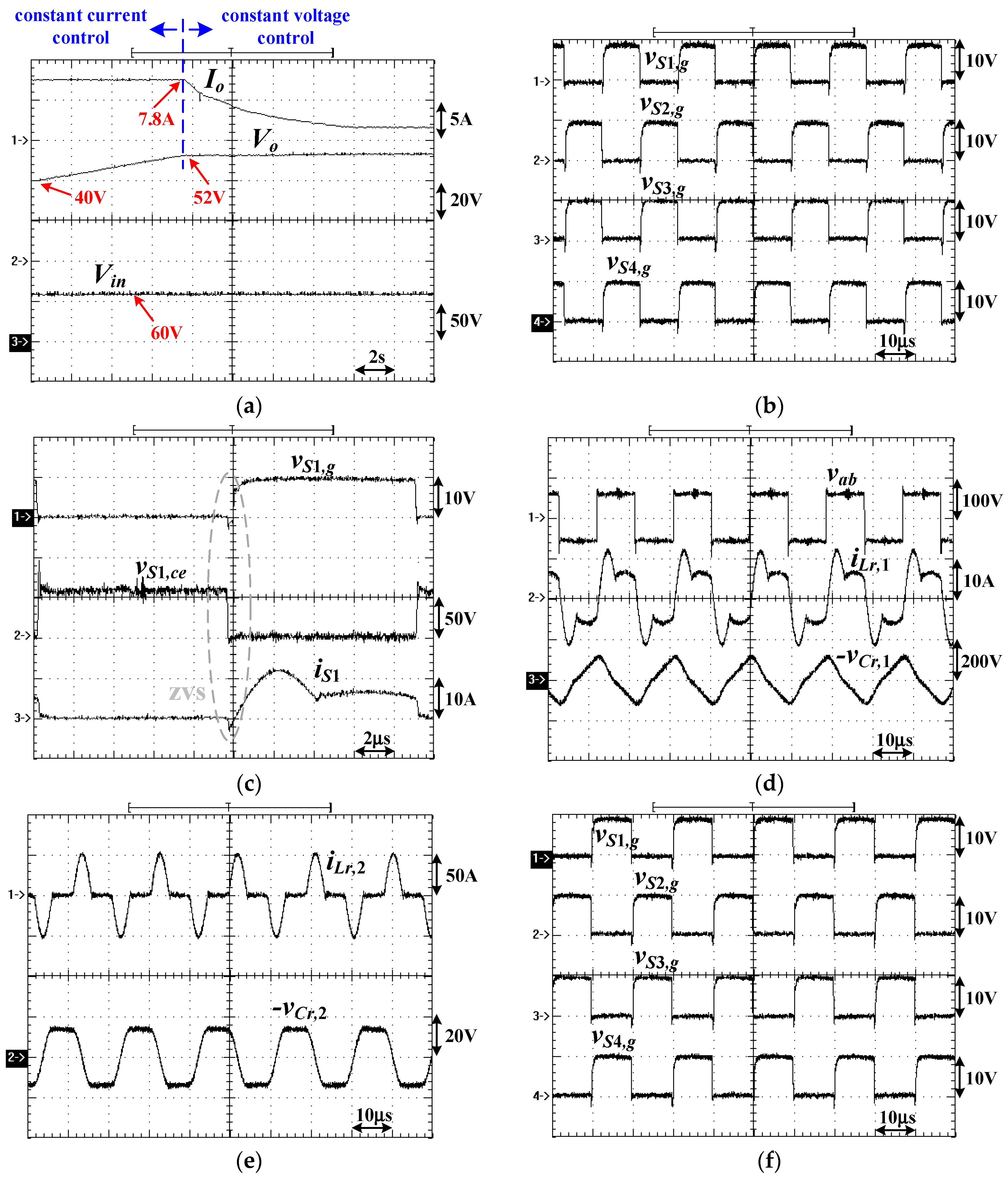
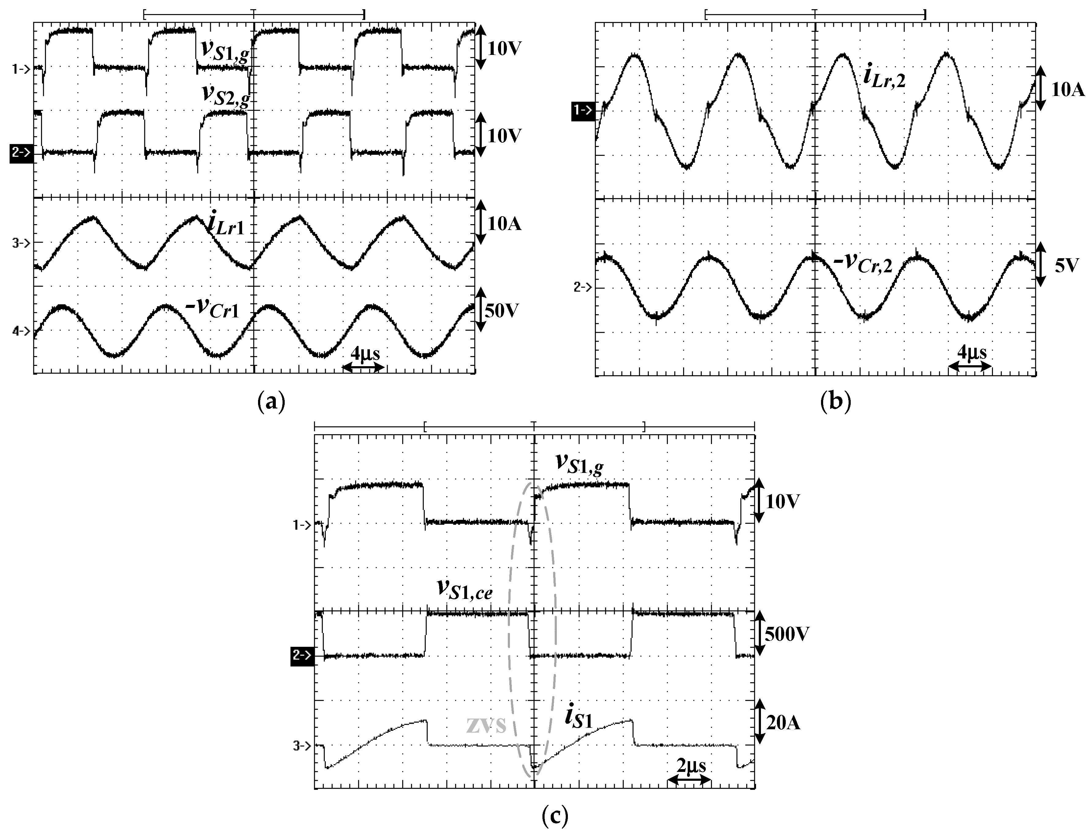
Figure 7 shows the measured input voltage Vin and the switch signals Sac1 and Sac2. It is clear that Sac1 is off and Sac2 is on when 60 V ≤ Vin < 120 V. The converter is operated at a low voltage range input, shown in Figure 1b. If 120 V ≤ Vin < 240 V, then Sac1 and Sac2 are both on, and the converter is operated at the medium voltage range input conditions, shown in Figure 1c. If 240 V ≤ Vin ≤ 480 V, then Sac1 is on and Sac2 is off and the converter is operated at the high voltage range input conditions, shown in Figure 1d. For forward power flow operation (battery charge), the constant current control (Io = 7.8 A) is selected to charge the battery (or load) from Vo = 40 V to 52 V. When the battery voltage reaches 52 V, then the constant voltage control (Vo = 52 V) is selected to charge battery. Figure 8a gives the measured load current, load voltage, and input voltage under Vin = 60 V and the forward power flow operation. When Vo is increased from 40 V and Vo ≤ 52 V, the load current Io is controlled at 7.8 A. If the load voltage is reached at 52 V, then the load voltage Vo is controlled at 52 V and the load current is redecreased from 7.8 A. Therefore, the maximum load power is at Vo = 52 V and Io = 7.8 A. Figure 8b–e show the measured results of the converter under Vin = 60 V, Io = 7.8 A, and Vo = 40 V conditions. The gate signals of S1–S4 are provided in Figure 8b. The switching frequency is about 55 kHz. The measured voltage and current of switch S1 are provided in Figure 8c. It is clear that S1 is turned on at zero-voltage switching. The experimental waveforms on the primary-side of the converter are given in Figure 8d. The leg voltage vab = ±Vin = ±60 V. Figure 8e shows the measured results of the resonant current and voltage on the secondary-side of the converter. When iLr,2 is positive (or negative), the voltage vCr,2 is increased (or negative). If iLr,2 = 0, then vCr,2 is kept at a constant value. Similarly, the measured results of the converter under Vin = 60 V, Io = 7.8 A, and Vo = 52 V (maximum power) conditions are given in Figure 8f–i.
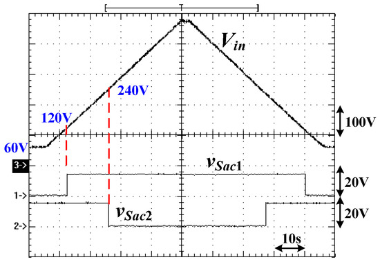
Figure 7.
Measured waveforms of Vin, Sac1, and Sac2.

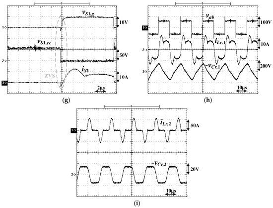
Figure 8.
Measured results of the proposed converter under Vin = 60 V: (a) load current, load voltage, and input voltage under a constant current or constant voltage control; (b) the gate voltages of S1–S4 under Vo = 40 V; (c) vS1,g, vS1,ce, and iS1 under Vo = 40 V; (d) vab, iLr,1, and –vCr,1 under Vo = 40 V; (e) iLr,2 and –vCr,2 under Vo = 40 V; (f) the gate voltages of S1–S4 under Vo = 52 V; (g) vS1,g, vS1,ce, and iS1 under Vo = 52 V; (h) vab, iLr,1; and –vCr,1 under Vo = 52 V; (i) iLr,2 and –vCr,2 under Vo = 52 V.
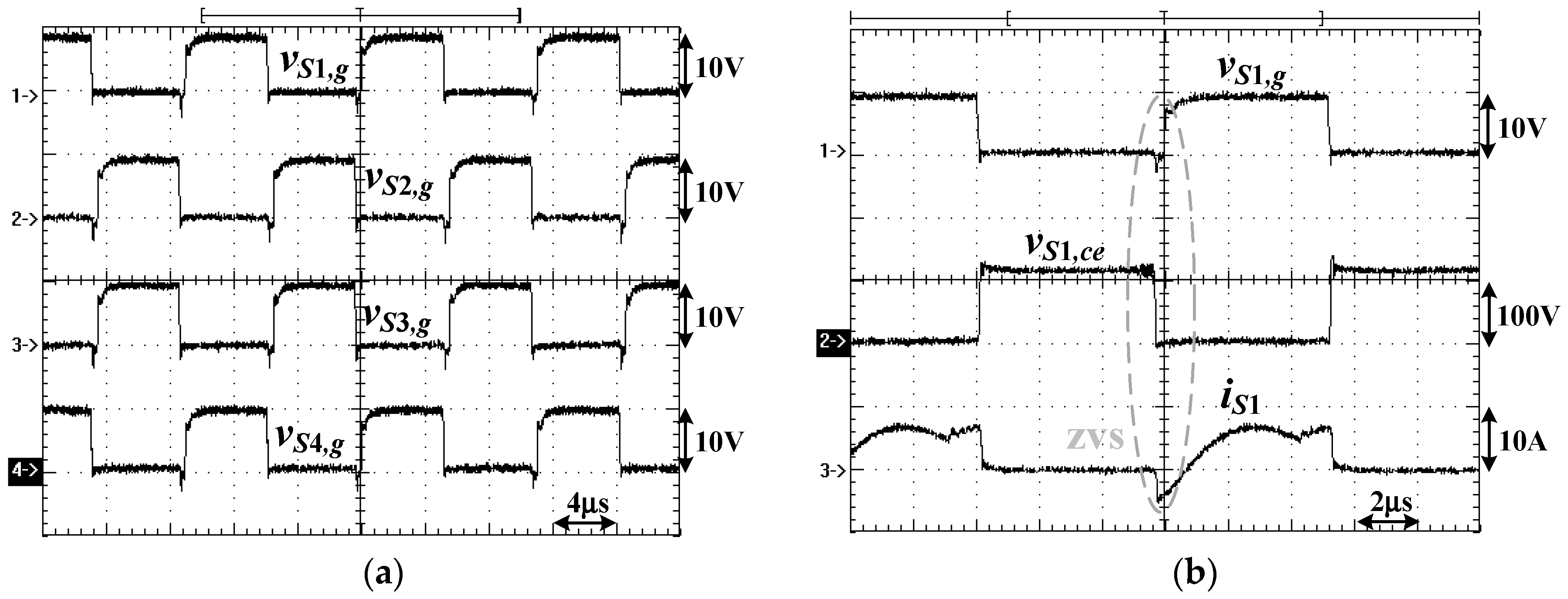
The measured results of the converter operated at Vin = 118 V and the maximum power (Io = 7.8 A and Vo = 52 V) condition are provided in Figure 9. From Figure 8 and Figure 9, one can observe that the converter has less voltage gain at Vin = 118 V so that the switching frequency of the converter at the Vin = 118 V condition is higher than the switching frequency at the Vin = 60 V condition. According to Figure 8c,g and Figure 9b, power switch S1 is turned on at zero-voltage switching for both the Vin = 60 V and 118 V cases.

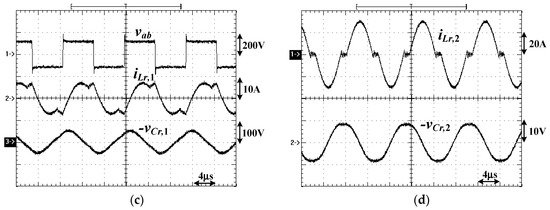
Figure 9.
Measured results of the proposed converter under Vin = 118 V, Vo = 52 V, and Io = 7.8 A: (a) the gate voltages of S1–S4; (b) vS1,g, vS1,ce, and iS1; (c) vab, iLr,1, and –vCr,1; (d) iLr,2 and –vCr,2.
Figure 10 gives the test results of the converter under Vin = 238 V and the maximum power conditions. The half-bridge resonant circuit and half-wave diode rectifier are used in the converter (Figure 1c) under Vin = 238 V input. Only switches S1 and S2 are controlled on the left-hand side. Figure 10a gives the gate voltages and resonant current and voltage on the input side. The resonant current and voltage on the output side are provided in Figure 10b. The switch voltage and current of S1 are provided in Figure 10c. The switching frequency of the converter at Vin = 238 V input and full power condition is about 96 kHz, which is close to the resonant frequency (100 kHz). The resonant currents iLr,1 and iLr,2 are quasi-sinusoidal waveforms. Power switch S1 is also turned on at zero-voltage switching under the Vin = 238 V condition (Figure 10c).
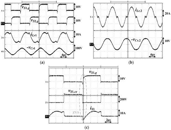
Figure 10.
Measured results of the proposed converter under Vin = 238 V, Vo = 52 V, and Io = 7.8 A: (a) vS1,g, vS2,g, iLr,1, and –vCr,1; (b) iLr,2 and –vCr,2; (c) vS1,g, vS1,ce, and iS1.
Figure 11 provides the experimental waveforms under Vin = 480 V and the maximum power conditions. The half-bridge resonant circuit and full-wave diode rectifier are used on the left-hanf side and right-hand side of the converter (Figure 1d) under the Vin = 480 V input. The waveforms vS1,g, vS2,g, iLr,1, and –vCr,1 are given in Figure 11a. The waveforms iLr,2 and –vCr,2 are provided in Figure 11b. The waveforms vS1,g, vS1,ce, and iS1 are shown in Figure 11c. The switching frequency of the converter at the Vin = 480 V input and maximum power condition is about 114 kHz. From the test results in Figure 11c, S1 is also turned on at zero-voltage switching under Vin = 480 V. For the backward power flow operation (from Vo to Vin), Vo = 52 V and Vin is controlled at 400 V. Therefore, S5–S8 are controlled on the right-hand side and the half-wave diode rectifier is operated on the left-hand side (Figure 1e). Figure 12 provides the experimental results under the backward power flow condition. Figure 12a shows the experimental waveforms vS5,g–vS8,g and the resonant currents and voltages are provided in Figure 12b. Figure 12c gives the test results of the switch current and voltage of S5. From the test results in Figure 12, the proposed converter can achieve reverse power flow operation well and switch S5 on the right-hand side can turn on at zero-voltage switching. The measured circuit efficiencies of the converter are 87.1%, 90.3%, 92.8%, and 93.6% at the Vin = 60 V, 118 V, 238 V, and 480 V inputs and maximum power conditions.
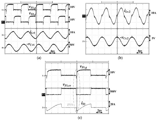
Figure 11.
Measured results of the proposed converter under Vin = 480 V, Vo = 52 V, and Io = 7.8 A: (a) vS1,g, vS2,g, iLr,1, and –vCr,1; (b) iLr,2 and –vCr,2; (c) vS1,g, vS1,ce, and iS1.
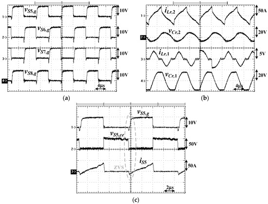
Figure 12.
Measured results of the proposed converter under backward power flow operation with Vo = 52 V and Vin = 400 V A: (a) vS5,g–vS8,g; (b) iLr,2, vCr,2, iLr,1, and vCr,1; (c) vS5,g, vS5,ce, and iS5.
6. Conclusions
In this paper, a hybrid resonant converter is presented and implemented to have wide voltage operation and forward/backward power flow operation for photovoltaic power or battery base applications. The symmetric resonant circuits with a half/full-bridge circuit structure are used on the primary and secondary side to achieve wide voltage operation, such as wide voltage variation on photovoltaic solar panel applications. By selecting the different circuit structures, such as half/full-bridge circuits, the converter can achieve different voltage gain under the input voltage condition. Thus, the drawback of conventional bidirectional resonant converters, such as a narrow voltage range operation, can be improved in the proposed converter. Owing to the resonant circuits on both the primary and secondary sides having the same resonant frequency, the bidirectional power flow can be easily implemented by using a pulse frequency modulation approach. In this paper, the basic circuit structure is presented and discussed in detail. The circuit operation and characteristics are also analyzed and provided. The circuit components of the laboratory prototype were designed, and the experiments are provided to show the benefits of the proposed converter.
Author Contributions
Data curation, Y.-Y.Z.; Formal analysis, B.-R.L.; Investigation, B.-R.L.; Methodology, B.-R.L.; Project administration, B.-R.L.; Validation, B.-R.L.; Writing—original draft, B.-R.L.; Writing—review & editing, B.-R.L. All authors have read and agreed to the published version of the manuscript.
Funding
This research is supported by the National Yunlin University of Science and Technology, Taiwan, under grant number 109H500311.
Acknowledgments
The authors thank the National Yunlin University of Science and Technology, Taiwan, for financial support under grant number 109H500311.
Conflicts of Interest
The authors declare no conflict of interest.
References
- Emadi, A.; Lee, Y.J.; Rajashekara, K. Power electronics and motor drives in electric, hybrid electric, and plug-in hybrid electric vehicles. IEEE Trans. Ind. Electron. 2008, 55, 2237–2245. [Google Scholar] [CrossRef]
- Dragicevic, T.; Lu, X.; Vasquez, J.C.; Guerrero, J.M. DC microgrids—Part I: A review of control strategies and stabilization techniques. IEEE Trans. Ind. Electron. 2016, 31, 4876–4891. [Google Scholar] [CrossRef] [Green Version]
- Dragicevic, T.; Lu, X.; Vasquez, J.C.; Guerrero, J.M. DC microgrids—Part II: A review of power architectures, applications, and standardization issue. IEEE Trans. Ind. Electron. 2016, 31, 3528–3549. [Google Scholar] [CrossRef] [Green Version]
- Guerrero, J.M.; Loh, P.C.; Lee, T.L.; Chandorkar, M. Advanced control architectures for intelligent microgrids—part II: Power quality, energy storage, and ac/dc microgrids. IEEE Trans. Ind. Electron. 2013, 60, 1263–1270. [Google Scholar] [CrossRef] [Green Version]
- Meng, L.; Shafiee, Q.; Trecate, G.F.; Karimi, H.; Fulwani, D.; Lu, X.; Guerrero, J.M. Review on control of DC microgrids and multiple microgrid clusters. IEEE J. Emerg. Sel. Top. Power Electron. 2017, 5, 928–948. [Google Scholar]
- Mangu, B.; Akshatha, S.; Suryanarayana, D.; Fernandes, B.G. Grid-connected PV-wind-battery-based multi-input transformer-couple bidirectional dc-dc converter for household applications. IEEE J. Emerg. Sel. Top. Power Electron. 2016, 4, 1086–1095. [Google Scholar] [CrossRef]
- Yilmaz, M.; Krein, P.T. Review of battery charger topologies, charging power levels, and infrastructure for plug-in electric and hybrid vehicles. IEEE Trans. Ind. Electron. 2013, 28, 2151–2169. [Google Scholar] [CrossRef]
- Ahrabi, R.R.; Ardi, H.; Elmi, M.; Ajami, A. A novel step-up multi input dc-dc converter for hybrid electric vehicles application. IEEE Trans. Ind. Electron. 2017, 32, 3549–3561. [Google Scholar]
- Tao, H.; Kotsopoulos, A.; Duarte, J.L.; Hendrix, M.A.M. Family of multiport bidirectional DC-DC converters. IEE Proc. Electr. Power Appl. 2006, 153, 451–458. [Google Scholar] [CrossRef] [Green Version]
- Xu, D.; Zhao, C.; Fan, H. A PWM plus phase-shift control bidirectional DC-DC converter. IEEE Trans. Ind. Electron. 2004, 19, 666–675. [Google Scholar] [CrossRef]
- Jain, A.K.; Ayyanar, R. PWM control of dual active bridge: Comprehensive analysis and experimental verification. IEEE Trans. Ind. Electron. 2011, 26, 1215–1227. [Google Scholar] [CrossRef]
- Zhao, B.; Song, Q.; Liu, W.; Sun, Y. Overview of dual-active-bridge isolated bidirectional DC–DC converter for high-frequency-link power-conversion system. IEEE Trans. Ind. Electron. 2014, 29, 4091–4106. [Google Scholar] [CrossRef]
- Rico, S.J.; Pagano, D.J.; Lucas, K.E. Bidirectional power sharing for DC microgrid enabled by dual active bridge DC-DC converter. Energies 2021, 14, 404. [Google Scholar]
- Lara, J.; Masisi, L.; Hernandez, C.; Arjona, A.; Chandra, A. Novel five-level ANPC bidirectional converter for power quality enhancement during G2V/V2G operation of cascaded EV charger. Energies 2021, 14, 2650. [Google Scholar] [CrossRef]
- Jung, J.H.; Kim, H.S.; Ryu, M.H.; Baek, J.W. Design methodology of bidirectional CLLC resonant converter for high-frequency isolation of DC distribution systems. IEEE Trans. Ind. Electron. 2013, 28, 1741–1755. [Google Scholar] [CrossRef]
- Zou, S.; Lu, J.; Mallik, A.; Khaligh, A. Bi-directional CLLC converter with synchronous rectification for plug-in electric vehicles. IEEE Trans. Ind. Appl. 2018, 54, 998–1005. [Google Scholar] [CrossRef]
- Shang, C.; Liu, L.; Liu, M.; Men, S. A highly-efficient two-stage DC-DC converter with wide input voltage. In Proceedings of the 2015 IEEE International Telecommunications Energy Conference, Osaka, Japan, 18–22 October 2015; pp. 1–6. [Google Scholar]
- Jeong, Y.; Kim, J.K.; Lee, J.B.; Moon, G.W. An asymmetric half-bridge resonant converter having a reduced conduction loss for DC/DC power applications with a wide range of low input voltage. IEEE Trans. Power Electron. 2017, 32, 7795–7804. [Google Scholar] [CrossRef]
- Lin, B.B.; Chen, K.Y. Hybrid LLC Converter with Wide Range of Zero-Voltage Switching and Wide Input Voltage Operation. Appl. Sci. 2020, 10, 8250. [Google Scholar] [CrossRef]
- Wang, P.; Zhou, L.; Zhang, Y.; Li, J.; Sumner, M. Input-parallel output-series DC-DC boost converter with a wide input voltage range, for fuel cell vehicles. IEEE Trans. Veh. Technol. 2017, 66, 7771–7781. [Google Scholar] [CrossRef]
- Hu, H.; Fang, X.; Chen, F.; Shen, Z.J.; Batarseh, I. A modified high-efficiency LLC converter with two transformers for wide input-voltage range applications. IEEE Trans. Power Electron. 2013, 28, 1946–1960. [Google Scholar] [CrossRef]
- Lin, B.R.; Dai, C.X. Wide Voltage Resonant Converter Using a Variable Winding Turns Ratio. Electronics 2020, 9, 370. [Google Scholar] [CrossRef] [Green Version]
- Steigerwald, R.L. A comparison of half-bridge resonant converter topologies. IEEE Trans. Power Electron. 1988, 3, 174–182. [Google Scholar] [CrossRef]


Publisher’s Note: MDPI stays neutral with regard to jurisdictional claims in published maps and institutional affiliations. |
© 2021 by the authors. Licensee MDPI, Basel, Switzerland. This article is an open access article distributed under the terms and conditions of the Creative Commons Attribution (CC BY) license (https://creativecommons.org/licenses/by/4.0/).