Abstract
The semiconductor manufacturing processes have been evolved to improve the yield rate. Here, we studied a sequential and comprehensive algorithm that could be used for fault detection and classification (FDC) of the semiconductor chips. A statistical process control (SPC) method is employed for inspecting whether sensors used in the semiconductor manufacturing process become stable or not. When the sensors are individually stable, the algorithm conducts the relational inspection to identify the relationship between two sensors. The key factor here is the coefficient of determination (R2). If R2 is calculated as more than 0.7, their relationship is analyzed through the regression analysis, while the algorithm conducts the clustering analysis to the sensor pair with R2 less than 0.7. This analysis also provided the capability to determine whether the newly generated data are defective or defect-free. Therefore, this study is not only applied to the semiconductor manufacturing process but can also be to the various research fields where the big data are treated.
1. Introduction
Advances in the semiconductor industry have enormously contributed to other contemporary high-innovative industries such as wireless communication, aerospace, and pharmaceutics [1,2,3]. Moreover, the semiconductor-based devices have a huge potential to achieve an advancement for wearables, robotics, and healthcare [4]. The emerge of smartphones has accelerated the development in the semiconductor industry and recently led to explosive demand in personal interest for Internet of Things (IoT) or home healthcare [5,6]. Biomedical microelectromechanical system (BioMEMS) is one of the representative areas that has progressed with the development of the semiconductor industry. Various biochips have previously been developed using the semiconductor fabrication process [7,8,9]. The front-end fabrication process of the semiconductor silicon chips was classified into seven main processes: photolithography, etching, deposition, chemical mechanical planarization, oxidation, ion implantation, and diffusion, as previously described [10]. When the back-end process (e.g., packaging of the die) and test step are considered, the whole process flow of the semiconductors can involve over 500 steps, which may require approximately 30–60 days [11,12]. The semiconductor industry has craved to identify the root causes of the faults in a real-time manner to reduce the process time and enhance the yield rate. However, the tremendous amounts of the data are generated during the long and complex semiconductor manufacturing process. The algorithm-based fault detection and classification (FDC) has been proposed in the previous studies [13,14]. The key challenge is an effective and rapid interpretation of the valuable information hidden in the vast and complex microfabrication data [15].
The FDC methods are commonly divided into three types: model-based, knowledge-based, and data-based methods, as previously described [16]. The model-based and knowledge-based methods have generally used for understanding the process input and output relationship through the mathematical calculation. However, the semiconductor manufacturing process is highly sophisticated. A huge number of sensors should be installed for measuring the physical quantities relevant to wafers’ status and the working environments (e.g., temperature, humidity, pressure, flow rate, and chemical gas flow) [17]. Although the model-based method has high accuracy, it is a time-consuming process to detect the adequate parameters in the complex semiconductor manufacturing processes. Additionally, the knowledge-based method often requires the skilled expertise and domain knowledge to make a relevant judgment on account of the correlation structure among faulty data. Therefore, the data-based method is more important to learn the process by monitoring historical data [18].
The statistical process control (SPC) has been employed to detect the wafer faults as a data-based method [19,20,21]. The SPC aims to illustrate the process variables and declare the abnormality based on the sensor data patterns. However, monitoring faults by the SPC is limited in inspecting the multiple variables. The multivariate analysis should be conducted for more effective fault detection at an early stage in the manufacturing process. For this analysis, the regression analysis and clustering method have widely been used in semiconductor manufacturing [22,23,24,25]. As the fault detection using regression analysis, the support vector regression (SVR) method has previously been reported [26]. The SVR was derived from a support vector machine (SVM) by being combined with regression analysis. The SVM have been used for the data classification [27]. The SVR was asserted to have outperformed any other methods using the regression analysis [28,29]. However, the SVR was only used for individual sensor inspection, not for figuring out the correlation between the two sensors. As a clustering method for the fault detection, the algorithm named dominant defective patterns finder (DDPfinder) has been proposed [25]. It clustered the patterns across the wafer and displayed wafer faults with Voronoi diagram based on the spatial dependencies. The DDPfinder showed excellent performance with respect to the accuracy, variance, and capability. Nevertheless, it has the complexity of the computational time due to spatial mapping of the faulty semiconductor chips on a wafer. In this paper, we proposed a sequential and comprehensive algorithm solution for detecting wafer faults. It could be comprehensively applied step by step from sensor stabilization to fault detection. Inspection methods used in this study involved the SPC, regression analysis, and clustering method. We focused on the classification to employ the most suitable inspections for each case. To reduce the computational time, we directly applied the clustering method to the data plane, not requiring mapping the data clustering on a wafer. Additionally, our algorithm divided the data plane into some regions through a Voronoi diagram, showing that the divided region could predict the faults of the semiconductor chips.
2. Materials and Methods
2.1. Algorithm Development
The overall workflow was categorized into three steps: preprocessing, inspection, and analysis (Figure 1). All steps were performed in Python 3.6 software (Python Software Foundation, Wilmington, NC, USA) using the scikit-learn library [30]. The sensor data were processed to be suitable for individual and relational inspection. The relational inspection consisted of clustering and regression analysis.
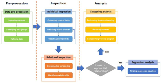
Figure 1.
Flow chart describing our proposed algorithm. The algorithm consisted of three steps: data preprocessing, individual and relational inspection, and clustering and regression analysis.
2.2. Data Preprocessing
The dataset used in this study was provided from Samsung Electronics Co., Ltd. (Suwon, Korea). It contained the sensor data for wafer preparation, which was recorded every 0.1 s, of virtually 30,000 wafers. Our dataset involved 25 processes, and each process took about 2 min. The total duration for the data collection including the time for initialization between processes was approximately 1 h 19 min and 12 s, and the whole data amount of each sensor was 47,520. The dataset contained 600 sensors named V001 to V600, which were categorized into two groups. One group was a constant sensor group associated with keeping the process condition for the safety. The whole process could stop as the output streams of the constant sensors discontinue. The other group was a non-constant sensor group, representing the current physical quantities of each process. This non-constant sensor group was also classified into peak and step sensors according to their output shapes. However, the step sensor group contained the sensors with too little variability. When any sensor value varies within ±0.2%, it was considered to be the constant sensor and its variation could be ignored as a noise, because the state with the variation within ±0.2% is defined as a steady state in a control system. Consequently, we classified the dataset into three groups: constant sensor, peak sensor, and step sensor (Figure 2A). The numbers of the sensors in each group are 535 (constant sensor), 22 (peak sensor), and 43 (step sensor). In this study, we focused on the peak sensor, because we could simply declare the faults by judging whether it was in a steady state or not for the constant and step sensors. However, there were no repetitive characteristics in the peak sensor group; in other words, a peak sensor represented the different outputs at each point of measurement. Such a difference could be generated due to the changes in other physical quantities; hence, we chose the relational analysis, such as the regression and clustering method. For the analysis of the peak sensors, we preprocessed the peak sensor data by extracting the peak value, which could be the most important value in the peak sensor. Algorithm 1 was developed to collect the peak data.
| Algorithm 1 For peak data collection |
| Input: peak sensor signal Output: indices 1: peakindex: = null; 2: peakvalue: = null; 3: Baseline: = running average (Sensor signal); 4: for index, value in signal do 5: if value > baseline then 6: if peak value == null or value> peak value then 7: peakindex: =index; 8: peakvalue: =sub peak value 9: else if peak value< baseline and peak index = null then 10: peak value: = abs peak; 11: end if 12: end if 13: end for 14: return |
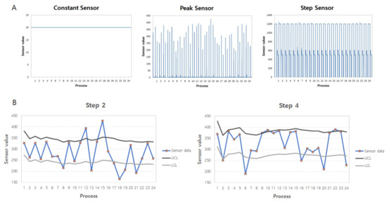
Figure 2.
Individual inspection for the sensor stabilization. (A) Classification of sensors. The sensor data were comprised of three types according to their output shape: constant, peak, and step sensor. (B) Outlier detection from the preprocessed data of a peak sensor (V009). The highest peak values were extracted at each step of the process. Since the peak of the V009 sensor appeared twice, the peak values were extracted at steps 2 and 4, respectively.
2.3. Individual Inspection
To investigate the fault of the individual wafer in the fabrication process, the SPC method was employed. The SPC included control charts known as process–behavior charts, which could be used to determine whether some process was out of control or not. We set two control lines for the control chart: upper control limit (UCL) and lower control limit (LCL). The data between UCL and LCL were regarded as normal data. In contrast, the data more than UCL or less than LCL were out of control. The types of control charts involved a X bar-chart, u-chart, p-chart, and c-chart. The c-chart can be used for counting the faults regardless of sample sizes. The formulas to calculate the c-chart are as follows [31]:
where is the mean during the control chart. For the real-time inspection, we employed a cumulated average value. The limit lines were changed as the process was progressed, and outliers could be detected based on the limit lines at that point (Figure 2B).
2.4. Regression Analysis
The relational inspection was used for identifying a relationship between two sensors. Since all the physical quantities were not independent and related to other physical quantities, the relational inspection should be considered. The linear and exponential relationships between two sensor data showed that the two data were interrelated under any physical or chemical laws. The regression analysis was useful for investigating such a relationship by finding an equation, known as a regression equation, that could elucidate the correlation between the two sensors. Based on the regression equation, we could detect the semiconductor faults by establishing a tolerance for this relation. For the training SVR, we generated some artificial outliers to represent the defect in the semiconductor manufacturing. The SVR was trained for each pair of sensors to detect the artificial outlier as a fault. An upper bound on the fraction of the training errors and a lower bound of the fraction of support vectors should be in the interval (0,1). In our study, the parameter ‘nu’ is 0.3 and ‘kernel’ is linear. To determine whether the two sensors are in correlation or not, the coefficient of determination (R2) is important. We can declare the correlation of the two sensors when their R2 is more than 0.7. This threshold R2 was based on the practical experience. When we performed the regression analysis by choosing any two sensors among our dataset, the results were clearly classified into two groups: below 0.3 and above 0.7.
2.5. Clustering Analysis
For other pairs except for the linear and exponential relations, the clustering analysis was conducted. We used a k-means clustering method. To group the data points in a k-means clustering, the centroids were arbitrarily placed on the data plane. The number (k) of the centroids was pre-defined to equal the number of the clusters. All of the data points should be associated with the closest centroid and the clusters formed as a group of associated data points with the same centroid. To evaluate these clusters’ intra-class similarity, the sum of squares (V) in the distance between every data point and associated centroid was calculated as follows [32]:
where is the j-th data point in the i-th cluster () and is the centroid of . This calculation was iterated as changing the centroid location. The next centroid was relocated on the center of the gravity among the data in the previous cluster.
The iteration was stopped when the clusters were no longer changed. We obtained the Voronoi diagram with the centroids of k-means clustering and determined the boundary of each cluster. The Voronoi diagram is a partition divided with the perpendicular bisector between a point and the closest one. This Voronoi diagram was implemented by Algorithm 2.
| Algorithm 2Sensor Defect Analysis Using Voronoi_k-Means (S, k) |
| Input: , where ( = 1, 2…25), a given set of peak sensor values, k (number of clusters) and Iters (iteration number) Output: (i) the optimal k means of clusters = 1, 2…k; and its Voronoi diagram (ii) the defect zone detection; Process: 1: Initialize the sensor dataset D = {, …} 2: Initialize cluster C = {, …} 3: Call Voronoi function V(S) 4: Initialize k cluster centroid = {, …} with k samples randomly picked from D 5: (); initialize clusters 6: (); initialize sensor number for each cluster 7: for j = 1, 2…k do 8: , M is the batch dataset and is the sample randomly picked from D 9: ; is cached cluster nearest to the data sample 10: end for 11: for m = 1, 2…b do; step 6 to step 8 are to cache the cluster centroid for each sample in the batch dataset. 12: ; get the catch centroid for 13: ; update sample number for each cluster centroid. 14: ; calculate learning rate for each cluster centroid. 15: ; take gradient step to update the cluster in each Voronoi space. 16: end for |
3. Results and Discussion
The individual inspection was performed for the stabilization of each sensor. We could clearly discern the process ready to be initiated when all sensors were in control normally. The software we developed in this study could inspect each sensor’s status through the SPC method. The V001 sensor was a timer representing the step change, showing that the process consisted of six steps (Figure 3A). V009 is exemplified for the peak sensor group, indicating the peak of which appeared twice: steps 2 and 4 (Figure 3B). Such an output was repetitive during the whole process. We separately extracted the peak at each step and applied the SPC method to each preprocessed data (Figure 2B). The fraction of the outlier over the dataset was 33.3% in both steps, respectively, during 25 processes. It might be in a stabilization where the sensor output could be fluctuated. When there was none of the data beyond UCL and LCL, we could proclaim the stable state. This SPC method made the process wait for the sensor output to become stable against time. As the sensor output becomes stable against time, the process gets the full-fledged initiation. Additionally, it helped to reduce the delay time of a wafer. Too long wafer delay time might damage the wafer due to the high temperature or dense chemical gas concentration [33]. This could become a trigger of some faults generated in the afterward manufacturing process. During the process, we assumed that the effect of time on the sensor output could be negligible as compared to the effect of the other property changes. At the end of every process, the initialization step (remarked as step 0) followed to become stable again.
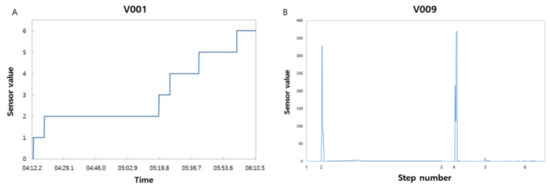
Figure 3.
Representation of each sensor value. (A) V001. (B) V009.
Some of the sensor pairs showed a correlation linearly or exponentially (Figure 4A). Such relations could be found in the semiconductor manufacturing process. For example, the thermal conductivity and electric conductivity were linearly related [34]. This relationship is called the conductivity-limiting phenomenon that the electric carrier mobility could control the bipolar thermal transport in semiconductors. Additionally, the mean energy of the electric carrier and electron concentration followed the Einstein relation . In this equation, is the diffusion coefficient, q is the electrical charge of a particle, is the mobility of the charged particle, is Boltzmann’s constant, and is the absolute temperature. This Einstein equation could be generalized for the semiconductor industry, which was a form of an exponential equation, as previously described [35]. For such correlated pairs, the faults could be found by mathematical calculations such as SVR.
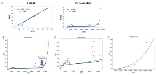
Figure 4.
Regression analysis to show the correlation between two sensors. (A) Grouping two sensors to observe whether they were correlated or not. Meaningful relationships in the semiconductor manufacturing process were linear and exponential. (B) Support vector regression method for the fault detection in the exponential relationship. This relationship could be divided into two sectors based on its threshold. The regression analysis was applied to the respective sector, (C) before and (D) after the threshold value.
For the exponential relationship, the additional data processing was required, because it showed the threshold value to activate the meaningful reaction in semiconductors. Before the threshold value, the sensor output linearly changed with a gentle slope. Upon reaching the threshold, an exponential increase appeared. To determine the threshold value, we investigated the slope. When the slope was suddenly increased, the data point was meant to be the threshold value. However, there were some data points out of control in the area before the threshold. The algorithm could misinterpret the defective data to be a threshold since a sudden increase appeared at that point. For this reason, we concentrated on the slope that showed continuously sudden increases at least twice. Therefore, we divided it into two sectors and separately conducted a regression analysis to each sector (sector1: before threshold, sector2: after threshold). In the case between V027 and V029, the threshold value was 11,108.39 in V027 value, and the regression equation was (R2 = 0.207) and (R2 = 0.882) in sectors 1 and 2, respectively. The R2 in sector 1 was too low, which indicates that V027 might be affected from other sensors besides V029 even when V029 did not activate. Such a case should be under more complex consideration. However, once V029 activated, V027 and V029 were highly correlated, showing that this regression equation was suitable for SVR. Therefore, we detected the faults using each regression equation in sector 2. The defect-free data points were marked in green and the defective data were marked in red. When the margin was set to be 0.3, the data in the area above 70 in V029 were detected as faults. Consequently, our algorithm detected four defective data in sector 2. Even in the case of more complex sensor pairs, it can also be represented through a linear, exponential relationship, or their combinational form. When equipped with complex mathematical calculation and expertise, it is possible to apply this method to other industries with more complex relationships.
For the non-correlated sensor pair, we applied a k-means clustering method with a Voronoi diagram. Actually, the choice of the similarity measures can highly affect the results of clustering. One might look at the sensor data in terms of the time-series data [36]. However, the time-series analysis is related to high-dimensional data, which involves some challenges: (i) the curse of dimensionality and (ii) difficulty in the graphical representation. A significant task to enhance the performances of the time-series is to reduce their dimensionality while preserving the main characteristics and reflect the original similarity of such data. When treating the time-series, the similarity between two sequences of the same length can be calculated by combining the ordered point-to-point distance between them. The most used distance function is the Euclidean distance, corresponding to other distance measuring methods. Thus, in our study, we chose the lower dimension data with the Euclidean point-to-point distance, while the higher dimensions allowed many-to-one point comparisons. In general, the fault detection using an algorithm suffered from the data imbalance problem, since most data should be defect-free in the process, as previously described [37]. Such an imbalance impacted the accuracy in that the algorithm could declare the defect-free to the defective data. To overcome this problem, the data processing techniques named over-sampling and under-sampling were introduced [38]. The over-sampling method could generate the artificial defect data along the line segment between other defective data. In contrast, the under-sampling method removes some defect-free data to match the numbers between the defective and defect-free data. First, we applied the k-means clustering to the data plane with the different k values (Figure 5). Then, we normalized the sensor data to convert the minimum and maximum value of each sensor into 0 to 100. This procedure prevents the misinterpretation caused due to a geometric distortion in the clustering map.
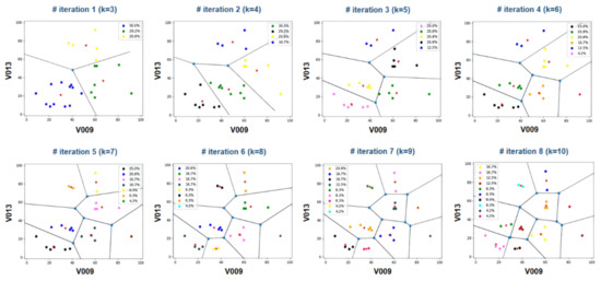
Figure 5.
Clustering method to understand the intra-class similarity between two non-correlated sensors. This clustering method was iterated with different k values (k = 3~10), standing for the number of clusters.
The data in the minority region were generally considered to be defective data, while the other data in the majority region were defect-free data. The optimized k value was 6, because the number of the data in the minority group was the same as the number of centroids in the majority group at k = 6. There were two minority groups (blue and pink dot) allocating 12.5% and 4.2%, respectively. The closest one from the centroid was determined as a representative data point in the majority group, and all data except for the representative data point were eliminated. As a result, the remaining data point consisted of only eight in the form of a balanced dataset. Four points were the representative data in the majority.
The group and the other four points were the original data in the minority group (Figure 6A,B). The Voronoi diagram was constructed on the processed clustering map. Each Voronoi region () is generally defined as follows [39]:
which means that is a group associated with the specific point based on the distance function . In other words, if a point x in space is nearer to than to other points (i.e., ), it could be gathered into the Voronoi region . For the distance function, we used Euclidean distance, which is the familiar distance function.
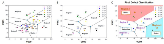
Figure 6.
Fault detection and classification using the clustering method. (A) Imbalanced dataset marking the data () and the centroid (). (B) Balanced dataset processed from the imbalanced dataset to match the amount of data in the minority group and the number of centroids in the majority group. (C) Final defect classification. When new data were generated, the algorithm determined whether the data had defects or were defect-free based on the region where the data were located.
According to its definition, we could use the Voronoi diagram to investigate the relevance to the standard data points and observe the faults afterward when new data came in (Figure 6C). If the newly generated data are located in the defective region, they can be classified as a defect. When the data generated in the defect-free region, it can be classified as defect-free. We employed a binary classification, consisting of ‘positive’ denoting the defect and ‘negative’ denoting the defect-free.
To evaluate the efficacy of our algorithm, we applied two general and intuitive methods; logistic regression (LR) [40] and one-class support vector machine (OCSVM) [41]. Using these two methods, we made the confusion matrixes (Figure 7) and calculated the evaluation metrics (Table 1). The evaluation metrics we used were accuracy, sensitivity, precision, and F1-score. Accuracy is the ratio of the data classified correctly over the whole data. Sensitivity is the ratio of the defect data classified correctly over whole actual defect data. Precision is the ratio of the defect data classified correctly over the whole data classified as the defect. F1-score is the harmonic mean of the sensitivity and precision. These metrics can be expressed as shown below:
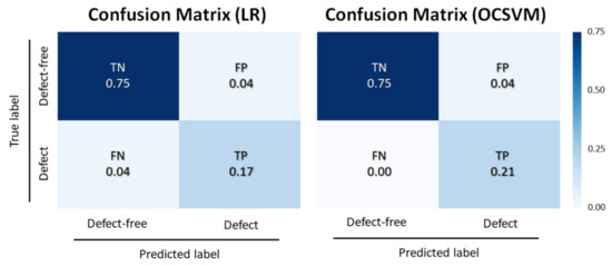
Figure 7.
Confusion matrix for a binary classification. The diagonal elements mean the data were classified correctly.

Table 1.
Performance comparison between LR and OCSVM methods.
In these equations, TP is a true positive (actual defect data classified as a defect). TN is a true negative (actual defect-free data classified as a defect-free). FP is a false positive (actual defect-free data classified as a defect). FN is a false negative (actual defect data classified as defect-free). Accordingly, we obtained the testing accuracy with 92% for LR and 96% for OCSVM. The results are comparable to related methods for FDC in the semiconductor manufacturing process [42,43].
The semiconductor manufacturing is a highly sophisticated and time-consuming process. In other words, there are too numerous root causes of the faults in the semiconductor manufacturing process, which is accompanied by the significant damage in the yield rate leading to cost and time losses when the wafer faults are found at the end of the processes. Thus, the FDC method in a real-time manner is demanded. There are classification methods that are capable of classifying raw data without the need for pre-treatment, such as independent component analysis (ICA) [44,45]. However, the data are not independently measured in the semiconductor manufacturing. As aforementioned, the tremendous amount of the data was generated in the semiconductor manufacturing, and they are complexly connected to each other. Hence, we suggested the algorithm for applying the different methods based on the characteristics of the sensor connection. The main factor to determine the applying method is whether the sensor pairs are correlated or not. To concentrate on the relational analysis, we eliminated other factors to cause the error and coded the algorithm for the sensor stabilization that keeps waiting until all sensors are in control. Our algorithm cannot be single-used for the semiconductor manufacturing process. However, it could contribute to a part of the FDC model in improving its efficiency and accuracy by revealing the relations between the highly numerous data.
4. Conclusions
We studied a sequential and comprehensive algorithm to observe the defects during the wafer preparation and the early stage of the semiconductor manufacturing process. Since the wafers are introduced and processed sequentially, the detection of the fault at the early stage of the semiconductor manufacturing process plays an important role in improving the yield rate for the quality control. Our algorithm integrated the SPC, regression analysis, and clustering method. This strategic approach provided each process with the most appropriate method according to the data status. We concentrated on studying the relationship between the data. Based on the coefficient of determination between two stabilized sensors, the algorithm can determine which approach can be employed among the regression analysis and the clustering method. This algorithm, which is advantageous in providing the hidden information among the complexly connected data, can become more powerful when combining other popular FDC models. Therefore, our algorithm, which observes the wafer defects at the early stage of the semiconductor manufacturing process, can be a promising solution to enhance the yield rate.
Author Contributions
Conceptualization, H.M. and T.H.K.; methodology, H.M. and J.M.L.; software, H.M. and T.H.K.; Validation, E.K., S.L., S.J. and B.G.C.; writing—original draft preparation, H.M. and T.H.K.; writing—review and editing, J.M.L., E.K., S.L., S.J. and B.G.C.; project administration, E.K., S.L., S.J. and B.G.C.; funding acquisition, B.G.C. All authors have read and agreed to the published version of the manuscript.
Funding
This work was supported by Samsung Electronics, the Sogang University Research Grant (Grant number 201970066.11) in Korea.
Institutional Review Board Statement
Not applicable.
Informed Consent Statement
Not applicable.
Data Availability Statement
The data presented in this study are available on request from the corresponding author.
Acknowledgments
We appreciate the sensor data obtained from Samsung Electronics in Korea.
Conflicts of Interest
The authors declare no conflict of interest.
References
- Shi, Y.; Zhou, Z.; Miao, X.; Liu, Y.J.; Fan, Q.; Wang, K.; Luo, D.; Sun, X.W. Circularly polarized luminescence from semiconductor quantum rods templated by self-assembled cellulose nanocrystals. J. Mater. Chem. C 2020, 8, 1048–1053. [Google Scholar] [CrossRef]
- Gohardani, A.S. Advances in Aerospace Engineering through Innovation in Packaging Design for High-Reliability Design Applications. In Proceedings of the 2018 AIAA SPACE and Astronautics Forum and Exposition, Orlando, FL, USA, 17–19 September 2018; p. 5224. [Google Scholar]
- Mekonnen, K.A.; Tangdiongga, E.; Koonen, A. High-capacity dynamic indoor all-optical-wireless communication system backed up with millimeter-wave radio techniques. J. Lightwave Technol. 2018, 36, 4460–4467. [Google Scholar] [CrossRef]
- Dahiya, A.S.; Shakthivel, D.; Kumaresan, Y.; Zumeit, A.; Christou, A.; Dahiya, R. High-performance printed electronics based on inorganic semiconducting nano to chip scale structures. Nano Converg. 2020, 7, 33. [Google Scholar] [CrossRef] [PubMed]
- Lee, J.-H.; Chae, E.-J.; Park, S.-J.; Choi, J.-W. Label-free detection of γ-aminobutyric acid based on silicon nanowire biosensor. Nano Converg. 2019, 6, 13. [Google Scholar] [CrossRef]
- Ulep, T.-H.; Yoon, J.-Y. Challenges in paper-based fluorogenic optical sensing with smartphones. Nano Converg. 2018, 5, 14. [Google Scholar] [CrossRef] [PubMed]
- Moarefian, M.; Davalos, R.V.; Tafti, D.K.; Achenie, L.E.; Jones, C.N. Modeling iontophoretic drug delivery in a microfluidic device. Lab Chip 2020, 20, 3310–3321. [Google Scholar] [PubMed]
- Li, X.; Huang, X.; Mo, J.; Wang, H.; Huang, Q.; Yang, C.; Zhang, T.; Chen, H.J.; Hang, T.; Liu, F. A Fully Integrated Closed-Loop System Based on Mesoporous Microneedles-Iontophoresis for Diabetes Treatment. Adv. Sci. 2021, 8, 2100827. [Google Scholar] [CrossRef] [PubMed]
- Azizi, M.; Davaji, B.; Nguyen, A.V.; Mokhtare, A.; Zhang, S.; Dogan, B.; Gibney, P.A.; Simpson, K.W.; Abbaspourrad, A. Biological small-molecule assays using gradient-based microfluidics. Biosens. Bioelectron. 2021, 178, 113038. [Google Scholar] [PubMed]
- Hollauer, C. Modeling of Thermal Oxidation and Stress Effects. Ph.D. Thesis, Technical University of Vienna, Vienna, Austria, 2007. [Google Scholar]
- Chien, C.-F.; Hsu, C.-Y.; Hsiao, C.-W. Manufacturing intelligence to forecast and reduce semiconductor cycle time. J. Intell. Manuf. 2012, 23, 2281–2294. [Google Scholar] [CrossRef]
- Hsieh, L.Y.; Hsieh, T.-J. A throughput management system for semiconductor wafer fabrication facilities: Design, systems and implementation. Processes 2018, 6, 16. [Google Scholar] [CrossRef]
- Lee, E.; Kim, T.H.; Lee, S.W.; Kim, J.H.; Kim, J.; Jeong, T.G.; Ahn, J.-H.; Cho, B. Improved electrical performance of a sol–gel IGZO transistor with high-k Al2O3 gate dielectric achieved by post annealing. Nano Converg. 2019, 6, 24. [Google Scholar] [PubMed]
- Ha, J.H.; Mazumdar, H.; Kim, T.H.; Lee, J.M.; Na, J.-G.; Chung, B.G. Algorithm analysis of gas bubble generation in a microfluidic device. BioChip J. 2019, 13, 133–141. [Google Scholar] [CrossRef]
- Chien, C.-F.; Wang, W.-C.; Cheng, J.-C. Data mining for yield enhancement in semiconductor manufacturing and an empirical study. Expert Syst. Appl. 2007, 33, 192–198. [Google Scholar] [CrossRef]
- Venkatasubramanian, V.; Rengaswamy, R.; Kavuri, S.N.; Yin, K. A review of process fault detection and diagnosis: Part III: Process history based methods. Comput. Chem. Eng. 2003, 27, 327–346. [Google Scholar] [CrossRef]
- Hsu, C.-Y.; Liu, W.-C. Multiple time-series convolutional neural network for fault detection and diagnosis and empirical study in semiconductor manufacturing. J. Intell. Manuf. 2021, 32, 823–836. [Google Scholar] [CrossRef]
- Vong, C.-M.; Wong, P.-K.; Ip, W.-F. A new framework of simultaneous-fault diagnosis using pairwise probabilistic multi-label classification for time-dependent patterns. IEEE Trans. Ind. Electron. 2012, 60, 3372–3385. [Google Scholar] [CrossRef]
- Ma, M.-D.; Wong, D.S.-H.; Jang, S.-S.; Tseng, S.-T. Fault detection based on statistical multivariate analysis and microarray visualization. IEEE Trans. Ind. Inform. 2009, 6, 18–24. [Google Scholar]
- Qin, S.J.; Cherry, G.; Good, R.; Wang, J.; Harrison, C.A. Semiconductor manufacturing process control and monitoring: A fab-wide framework. J. Process Control 2006, 16, 179–191. [Google Scholar] [CrossRef]
- Yue, H.H.; Qin, S.J.; Markle, R.J.; Nauert, C.; Gatto, M. Fault detection of plasma etchers using optical emission spectra. IEEE Trans. Semicond. Manuf. 2000, 13, 374–385. [Google Scholar] [CrossRef]
- Wang, J.; Zhang, J.; Wang, X. A data driven cycle time prediction with feature selection in a semiconductor wafer fabrication system. IEEE Trans. Semicond. Manuf. 2018, 31, 173–182. [Google Scholar] [CrossRef]
- Hong, A.; Chen, A. Piecewise regression model construction with sample efficient regression tree (SERT) and applications to semiconductor yield analysis. J. Process Control 2012, 22, 1307–1317. [Google Scholar] [CrossRef]
- Zhou, Z.; Wen, C.; Yang, C. Fault detection using random projections and k-nearest neighbor rule for semiconductor manufacturing processes. IEEE Trans. Semicond. Manuf. 2014, 28, 70–79. [Google Scholar]
- Taha, K.; Salah, K.; Yoo, P.D. Clustering the dominant defective patterns in semiconductor wafer maps. IEEE Trans. Semicond. Manuf. 2017, 31, 156–165. [Google Scholar] [CrossRef]
- Purwins, H.; Barak, B.; Nagi, A.; Engel, R.; Höckele, U.; Kyek, A.; Cherla, S.; Lenz, B.; Pfeifer, G.; Weinzierl, K. Regression methods for virtual metrology of layer thickness in chemical vapor deposition. IEEE/ASME Trans. Mechatron. 2013, 19, 1–8. [Google Scholar]
- Mazumdar, H.; Kim, T.H.; Lee, J.M.; Ha, J.H.; Ahrberg, C.D.; Chung, B.G. Prediction analysis and quality assessment of microwell array images. Electrophoresis 2018, 39, 948–956. [Google Scholar] [PubMed]
- Wang, J.; Yang, Z.; Zhang, J.; Zhang, Q.; Chien, W.-T.K. AdaBalGAN: An improved generative adversarial network with imbalanced learning for wafer defective pattern recognition. IEEE Trans. Semicond. Manuf. 2019, 32, 310–319. [Google Scholar]
- Kim, E.; Cho, S.; Lee, B.; Cho, M. Fault detection and diagnosis using self-attentive convolutional neural networks for variable-length sensor data in semiconductor manufacturing. IEEE Trans. Semicond. Manuf. 2019, 32, 302–309. [Google Scholar]
- Pedregosa, F.; Varoquaux, G.; Gramfort, A.; Michel, V.; Thirion, B.; Grisel, O.; Blondel, M.; Prettenhofer, P.; Weiss, R.; Dubourg, V. Scikit-learn: Machine learning in Python. J. Mach. Learn. Res. 2011, 12, 2825–2830. [Google Scholar]
- Kittlitz, R.G., Jr. Calculating the (almost) exact control limits for a C-chart. Qual. Eng. 2006, 18, 359–366. [Google Scholar] [CrossRef]
- Kubo, T.; Ino, T.; Minami, K.; Minami, M.; Homma, T. A statistical process control method for semiconductor manufacturing. SICE J. Control Meas. Syst. Integr. 2009, 2, 246–254. [Google Scholar] [CrossRef][Green Version]
- Xiong, W.; Pan, C.; Qiao, Y.; Wu, N.; Chen, M.; Hsieh, P. Reducing wafer delay time by robot idle time regulation for single-arm cluster tools. IEEE Trans. Autom. Sci. Eng. 2020, 18, 1653–1667. [Google Scholar] [CrossRef]
- Wang, S.; Yang, J.; Toll, T.; Yang, J.; Zhang, W.; Tang, X. Conductivity-limiting bipolar thermal conductivity in semiconductors. Sci. Rep. 2015, 5, 10136. [Google Scholar] [CrossRef] [PubMed]
- Jyegal, J. Thermal energy diffusion incorporating generalized Einstein relation for degenerate semiconductors. Appl. Sci. 2017, 7, 773. [Google Scholar] [CrossRef]
- Berndt, D.J.; Clifford, J. Using dynamic time warping to find patterns in time series. In Proceedings of the KDD Workshop, Seattle, WA, USA, 31 July–1 August 1994; pp. 359–370. [Google Scholar]
- Henein, M.M.; Shawky, D.M.; Abd-El-Hafiz, S.K. Clustering-based Under-sampling for Software Defect Prediction. In Proceedings of the ICSOFT, Porto, Portugal, 26–28 July 2018; pp. 219–227. [Google Scholar]
- Puntumapon, K.; Rakthamamon, T.; Waiyamai, K. Cluster-based minority over-sampling for imbalanced datasets. IEICE Trans. Inf. Syst. 2016, 99, 3101–3109. [Google Scholar]
- Küng, J.; Wagner, R. Transactions on Large-Scale Data-and Knowledge-Centered Systems I.; Springer: New York, NY, USA, 2009. [Google Scholar]
- Preuveneers, D.; Joosen, W. Sharing Machine Learning Models as Indicators of Compromise for Cyber Threat Intelligence. J. Cybersecur. Priv. 2021, 1, 140–163. [Google Scholar] [CrossRef]
- Lee, J.-I.; Kim, D.-H.; Yoo, H.-J.; Choi, H.-G.; Lee, Y.-S. Comparison of the Predicting Performance for Fate of Medial Meniscus Posterior Root Tear Based on Treatment Strategies: A Comparison between Logistic Regression, Gradient Boosting, and CNN Algorithms. Diagnostics 2021, 11, 1225. [Google Scholar] [CrossRef]
- Wen, G.; Gao, Z.; Cai, Q.; Wang, Y.; Mei, S. A novel method based on deep convolutional neural networks for wafer semiconductor surface defect inspection. IEEE Trans. Instrum. Meas. 2020, 69, 9668–9680. [Google Scholar] [CrossRef]
- O’Leary, J.; Sawlani, K.; Mesbah, A. Deep learning for classification of the chemical composition of particle defects on semiconductor wafers. IEEE Trans. Semicond. Manuf. 2020, 33, 72–85. [Google Scholar]
- Greco, A.; Costantino, D.; Morabito, F.; Versaci, M. A Morlet wavelet classification technique for ICA filtered SEMG experimental data. In Proceedings of the International Joint Conference on Neural Networks, Portland, OR, USA, 20–24 July 2003; pp. 166–171. [Google Scholar]
- Xia, J.; Bombrun, L.; Adalı, T.; Berthoumieu, Y.; Germain, C. Spectral–spatial classification of hyperspectral images using ICA and edge-preserving filter via an ensemble strategy. IEEE Trans. Geosci. Remote Sens. 2016, 54, 4971–4982. [Google Scholar]
Publisher’s Note: MDPI stays neutral with regard to jurisdictional claims in published maps and institutional affiliations. |
© 2021 by the authors. Licensee MDPI, Basel, Switzerland. This article is an open access article distributed under the terms and conditions of the Creative Commons Attribution (CC BY) license (https://creativecommons.org/licenses/by/4.0/).