Article

Simulation of On-Chip Broadband Photon Spin Router Base on Nondiffracting Surface Plasmon Beam Launching

1
Photonics Research Center, Guilin University of Electronic Technology, Guilin 541004, China
2
Guangxi Key Laboratory of Optoelectronic Information Processing, Guilin University of Electronics Technology, Guilin 541004, China
3
Guangxi Key Laboratory of Automatic Detecting Technology and Instrument, Guilin University of Electronics Technology, Guilin 541004, China
*
Author to whom correspondence should be addressed.
Appl. Sci. 2021, 11(22), 10643; https://doi.org/10.3390/app112210643
Submission received: 13 October 2021 / Revised: 7 November 2021 / Accepted: 8 November 2021 / Published: 11 November 2021

Abstract

:
The development of a photonic device based on a non-diffracting surface plasmon polariton (SPP) beam can effectively improve the anti-interference ability. Furthermore, an easily adjustable on-chip routing device is highly desirable and extremely important in practical optical communication applications. However, no non-diffracting SPP-beam-based spin routing devices with high tunability in multiple degrees of freedom have been reported. In this study, we theoretically designed a simple micro-nano structure to realize a highly adjustable non-diffracting SPP-beam-based spin router using Finite-Difference Time-Domain (FDTD) simulation. The simulation results show that the structure enables spin-controlled nondiffracting SPP-beam directional launching. The launching direction of the nondiffracting SPP beam can be dynamically rotated counterclockwise or clockwise by changing the incident angle. Hence, the routing SPP beam can be coupled to different output waveguides to provide dynamic tunability. Moreover, this device shows good broadband response ability. This work may motivate the design and fabrication of future practical photon routing devices.

1. Introduction

Due to the strong light-electron coupling at the interface of a metal and a medium, surface plasmon polaritons (SPPs) have enticing properties, such as the subwavelength confinement and surface enhancement of the optical field. Due to the benefits provided by these features, SPPs are widely used in designing on-chip photonics devices, such as optical switches [1], optical logical gates [2,3], and other optical parameter detecting devices [4,5], which will be important in future information processing and all optical communication. In these planar-integrated nanophotonics devices, on-chip manipulation and control of SPPs is of crucial importance. Therefore, a large number of studies have been conducted regarding the control of SPPs on metal surfaces with well-designed nanostructures [6,7,8] by manipulating optical parameters such as wavelength [9], phase [10,11,12], and polarization state [13,14,15] of the incident light. An optical router is an important component in communication systems. When designing optical routing devices for signal transmission, in general, the aim is to uniquely connect a certain launching path of the excited optical signal with a certain optical state of the incident signal. Therefore, the light parameters, such as wavelength and polarization state, which determine the SPPs’ directional launching, are the key functionality for designing SPP-based on-chip photon routing devices. In 2013, Jiao Lin et al. reported that the polarization-sensitive plasmonic apertures having the shape of an ear of wheat in a gold film enabled polarization-controlled tunable SPP directional launching [16]. Since then, controllable SPP directional launching [17,18,19,20] and on-chip spin routing devices [21,22,23] have received significant research attention. However, most reported works have only realized two possible SPP directional launching paths by controlling the polarization states of the incident light, which limits the tunability. Developing highly adjustable on-chip routing devices is extremely important in practical applications. By comparison, in previous works [17,18,19,20], the directional launching SPPs suffer from beam diffraction during the propagation. Suppressing this diffraction can effectively improve the anti-interference ability. Thus, the suppression of the on-chip SPP-beam diffraction effect has become a popular research topic in recent years. One of the most effective and feasible solutions is to excite a non-diffracting SPP beam. Although a large number of investigations on non-diffracting SPP beams have been undertaken [24,25,26,27,28], to the best of our knowledge, non-diffracting SPP-beam-based spin routing devices with high tunability in multiple degrees of freedom have not been reported.
Therefore, this study focused on the highly adjustable non-diffracting SPP-beam-based spin router. A simple rectangle nano-slot array structure, which can generate a nondiffracting SPP beam in the positive/negative y-axis direction when the incident light undergoes left circular polarization (LCP)/right circular polarization (RCP), was theoretically designed to realize spin routing using Finite-Difference Time-Domain (FDTD) simulation. The simulation results show that the propagation direction of the excited nondiffracting SPP beam can be dynamically rotated counterclockwise or clockwise by changing the incident angle. Hence, the routing SPP beam can be coupled to different output waveguides to realize dynamic tunability. The broadband response of the device was also investigated.

2. Principle and Simulation Results

The 3D structure diagram of our device is shown in Figure 1a and the 2D structure diagram is shown in Figure 1b. To realize the polarization-controlled SPP launching, the basic structure of the device consists of two parallel columns of a nano-rectangular slot with width W and length L, which are etched on a gold film. The distance between the center points of the two adjacent slots on different columns is S 2 + ( D / 2 ) 2 , where S is the perpendicular distance of the two columns and D is the distance between the center points of the two adjacent slots on one column. When D is shorter than the effective wavelength of the SPPs ( λ s p p ), the columns will generate a quasi-plane SPP wave. For the case of plane wave incidence, only the component polarized perpendicular to the long side of the nano-rectangular slot can significantly excite the SPPs. Therefore, the initial phase of the SPPs generated by a single rectangle slot depends on its orientation angle α and the handedness of the incident light. This is the so-called Pancharatnam–Berry (PB) phase [29], which is given by ϕ ( α ) = σ ± [ α s g n ( α ) π 2 ] , where σ ± is the spin quantum number, i.e., σ + = 1 represents LCP and σ = 1 represents RCP; sgn() is the sign function; and α ( π , π ) is the polar angle of the orientation direction of the nano-rectangular slot in the local coordinate system ( x , y ) (see Figure 1b). Thus, under LCP incidence and slot parameters of α 1 = π 4 and α 2 = π 4 , for the SPP waves propagating to the left side of the columns, the phase difference between the SPPs exited on column 1 and column 2 is Δ ϕ l e f t = k s p p S π 2 , whereas for the SPP waves propagating to the right side of the columns, the phase difference between the SPPs exited on column 1 and column 2 is Δ ϕ r i g h t = k s p p S + π 2   , where kspp represents the wavevector of the SPP, and k s p p = 2 π λ s p p . If we design S = λ s p p 4 , the phase difference will be Δ ϕ l e f t = 0 and Δ ϕ r i g h t = π . This means that the SPPs wave will generate constructive interference on the left side of the columns and destructive interference on the right side. Similarly, when the incident light is RCP, the opposite happens. In this way, we can realize different directions of SPP launching under different circular polarization excitations. If the columns have a slant angle θ with the y-axis, the propagation direction of the SPP plane wave will have the same angle with the x-axis. To realize nondiffracting SPP-beam excitation, an aperture structure consisting of an upper subarray with slant angle θ and a lower subarray with the slant angle θ was designed, as shown in the inset of Figure 2a. The structure can generate a cosine–Gauss SPP beam [30], which is a kind of novel nondiffracting beam. This is demonstrated by the FDTD simulation result given in Figure 2a, which shows a nondiffracting SPP beam launching along the negative x-axis under LCP incidence. This is because, when the incident light is LCP, the SPP beams excited on the upper and lower subarray launch toward the left side and converge on the negative x-axis. Then, the constructive interference of the two converging SPP beams generates the nondiffracting SPP beam. In the simulation, the incident light is a plane wave with LCP, the light wavelength ( λ 0 ) is 633 nm, and the dielectric constant of the gold is −11.8351 + 1.24102i. Hence, the wavelength of the SPPs is λ s p p = λ 0 ( ε m + ε d ) / ( ε m ε d ) = 605.67 nm , where ε m is the real part of the permittivity of metal and ε d is the permittivity of the dielectric medium (i.e., air). The mesh precision of the FDTD model is 10 nm, the boundary condition is a perfect match layer (PML), and the simulation parameters are h = 120   nm ,   W = 40   nm ,   L = 200   nm ,   S = 150   nm and D = 300   nm . The value of the slant angle θ is 10° and every column has 13 nano-rectangular slots. Obviously, in this aperture structure (the inset of Figure 2a), when the incident light is RCP, the SPP beams excited on the upper and lower subarray will launch toward the right side and cannot converge, and hence cannot generate a nondiffracting SPP beam in this case. Therefore, in order to launch a nondiffracting SPP beam in different directions under different circular polarization incidences, a symmetric pair of subarrays should be etched on the gold film, shown as the inset of Figure 2b. Figure 2b shows the simulated SPP intensity distribution result of this structure under LCP incidence. The result shows that, although the participation of the symmetric pair results in some side lobes, it will not affect the non-diffraction characteristic of the main lobe of the SPP beam. As this structure (the inset of Figure 2b) is mirror symmetric, it is easy to know that it will launch a nondiffracting SPP beam along the positive x-axis under RCP incidence. Hence, we can realize a nondiffracting SPP-beam launching-based spin router. In the simulation of Figure 2b, the distance ( δ , see the inset of Figure 2b) between the left and right symmetric structures is δ = 5   μ m and the other parameters are that same as those used in Figure 2a.
We then chose the transversal electric field intensity distributions at x = ± 13   μ m , shown in Figure 2c, to observe the intensity distribution of the nondiffracting SPP beam. It can be found that the transversal electric field intensity distributions are similar to the cosine–Gauss-like beam [30]. We found that the intensity distribution is slightly asymmetrical with the x-axis. This is because the subarrays are not symmetrical with the x-axis. The key point of a nondiffracting SPP beam in improving the anti-interference ability of photonic devices is that when there is an obstacle on the propagation path, the SPP beam can effectively bypass the obstacle and continue to propagate. This self-healing ability of our device is demonstrated by the FDTD simulation result of Figure 2d, in which a gold cylinder with a radius of 150 nm is set on the propagation path at the point of coordinate (−13 μm, 0) as an obstacle. Obviously, although the obstacle causes the SPPs to diverge, the SPP beam will return to being nondiffracting behind the obstacle. Thus, the proposed structure can improve the anti-interference ability of the photonic device. In addition, the tunability of a device is very important in practical applications. Hence, realizing tunable nondiffracting SPP-beam launching is expected in our device. For this, we investigated the influence of the incident angle on the SPP launching direction. If the light is incident at an inclined angle γ with the z-axis in the y-z plane, it carries an in-plane wave vector k i n = k 0 sin ( γ ) , where k 0 is the free-space wave vector of the incident light. This extra wave vector will change the SPP-beam launching direction [31,32].
Figure 3 illustrates how kin influences the nondiffracting SPP-beam launching direction when the incident light has an inclined angle with the z-axis in the y-z plane. In the figure, the line segments OP and OQ, respectively, are the equiphase lines of the SPP beams excited by the upper and lower nano-rectangular slot arrays when γ = 0 ; the line segments O P and O Q , respectively, are the equiphase lines of the SPP beams excited by the upper and lower nano-rectangular slot arrays when γ 0 ; OF is the nondiffracting SPP-beam launching direction when γ = 0 ; and O F is the nondiffracting SPP-beam launching direction when γ 0 . It can be easily seen that under γ 0 , the equiphase lines of the SPP beams excited by the upper and lower nano-rectangular slot arrays ( O P and O Q ) are rotated counterclockwise with respect to the equiphase lines under γ = 0 by β , which is given by:
β = arcsin ( k o sin ( γ ) cos ( θ ) k s p p ) .
In this case, the main lobe of the nondiffracting SPP beam will be located on the red dashed line of Figure 3, which has an angle β with the x-axis. Figure 4a–d shows the results of modulating the SPP-beam launching direction by changing γ . We can observe that when the inclined angle is 5° and −5°, the main lobe of the nondiffracting SPP beam is inclined without destroying its nondiffracting property, and the inclined angle of the nondiffracting SPP beam is approximately 5°, which shows good agreement with the calculation result of the equation.
We then further extracted the transversal electric field intensity distributions at x = ± 13   μ m when the incident light is LCP and RCP, respectively. The results are shown in Figure 5a. The figure shows that, despite the change in the inclined angle of the incident light, the intensity distribution curves still approximate the cosine–Gauss distribution and have good consistency for the incident light with different polarization states. However, because the aperture array is not symmetrical with the x-axis, both the intensity and transverse displacement of the main lobe maximum strength point under γ = 5 ° are slightly larger than those under γ = 5 ° . The self-healing ability of the main lobe of the SPP beam is also demonstrated by setting a gold cylinder with a radius of 150 nm at the point of coordinate (13 μm, 0.94 μm) under RCP incidence and inclined angle γ = 5 ° (see Figure 5b). Hence, it is demonstrated that, in practical applications, the SPP launching directions can be effectively regulated by controlling γ without destroying its nondiffracting property.

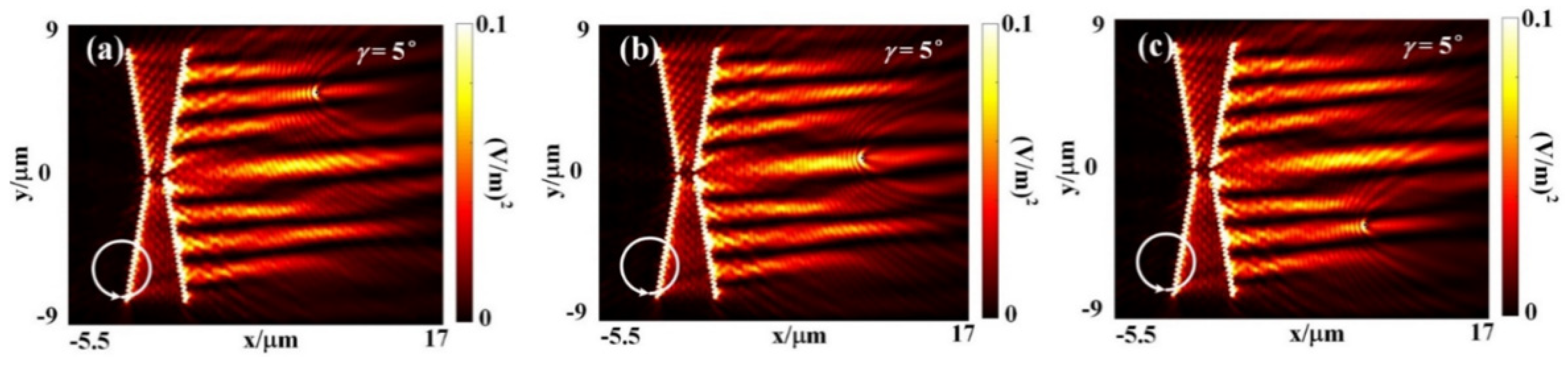
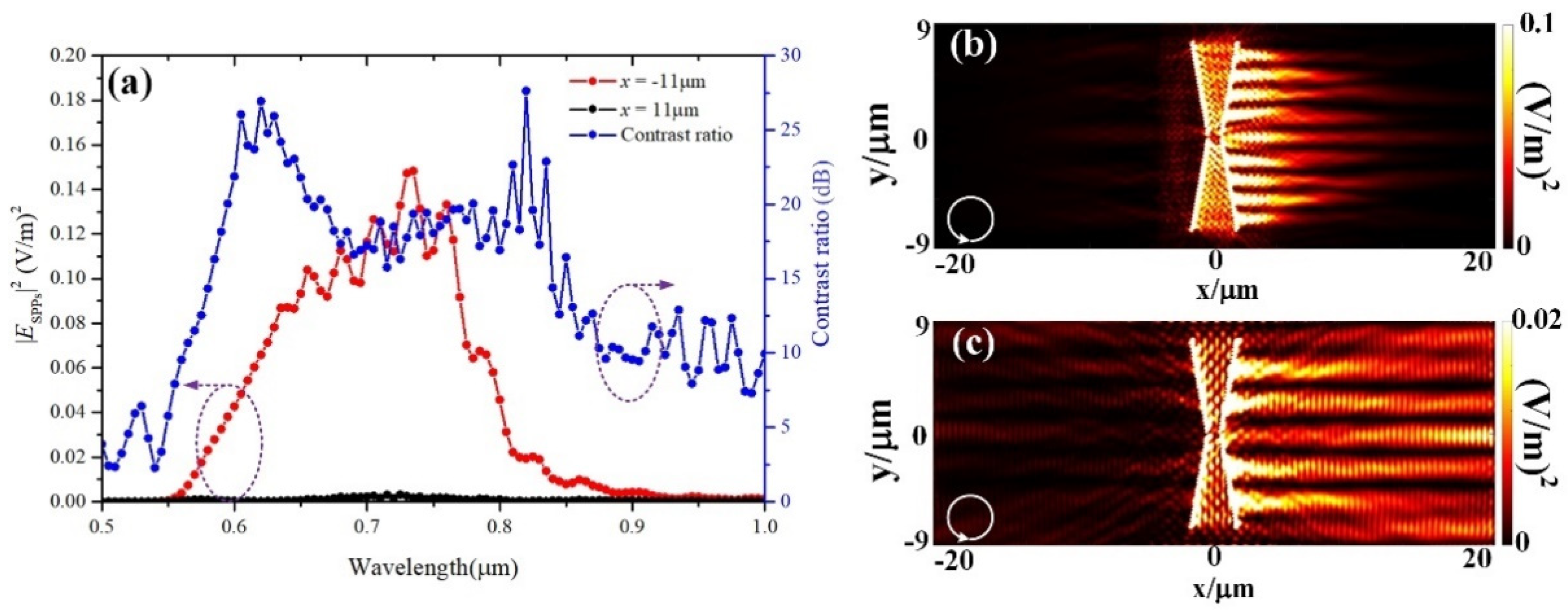
3. Multi-Nondiffracting SPP-Beam Launching

The above results of the intensity distribution indicate that some sidelobes exist beside the main lobe of the nondiffracting SPP beam. It is obvious that these sidelobes are induced by the interference of the SPP electric field generated by different subarrays located on different sides of the y-axis. By properly controlling the distance between the two subarrays on different sides of the y-axis and the length of the subarrays, we found that the overlapping region of the SPP beams generated by different subarrays located on different sides of the y-axis can be enlarged and the sidelobes can be converted into a new nondiffracting SPP beam. Therefore, this provides an opportunity to realize multichannel nondiffracting SPP-beam directional launching. To demonstrate this, by reducing the distance between the subarrays on different sides of the y-axis and extending their length appropriately, we realized directional launching of three nondiffracting SPP beams. The FDTD simulation results are shown in Figure 6. In the simulation, the distance between the two subarrays on the different sides of the y-axis is δ = 1 μm, every column has 25 nano-rectangular slots, and the other parameters are the same as those used in Figure 2a. It can be seen that there are three nondiffracting SPP beams when the incident light is LCP and RCP. Because the distance between the two subarrays on the different sides of the y-axis does not affect the propagating direction of the SPP wave, the nondiffracting SPP-beam launching direction remains unchanged when adjusting the distance (see Figure 6a). We then further extracted the transversal electric field intensity distributions at x = ± 11   μ m , which are shown in Figure 6b. Figure 6c–f shows the results of modulating the three SPP-beam launching directions by changing γ . We can observe that when the incidence inclined angle is 5° and −5°, the inclined angle of the three nondiffracting SPP beams is approximately 5°.
The figure shows that the nondiffracting property is maintained when we regulate the three SPP-beam launching directions by controlling γ . The incident of RCP light under an inclined angle γ = 5 ° was selected as an example to detect the self-healing ability of the three nondiffracting SPP beams. We placed a gold cylinder obstacle with a radius of 150 nm at the points (10 μm, 4.96 μm), (11 μm, 0.90 μm), and (10 μm, −3.33 μm) to simulate the SPP intensity distribution. The FDTD simulation results are shown in Figure 7. It can be seen that all three directional launching SPP beams have self-healing ability after the obstacle.
Considering that the broadband response of a device is expected in practical applications, we further simulated the response of our multichannel nondiffracting SPP-beam launching device in a broadband wavelength range. We chose the two points of (−11 μm, 0) and (11 μm, 0) on the two main SPP intensity lobes under different circular polarization incidences as observation points to observe the directional launching ability of this device, and used the contrast ratio of the two observation points’ SPP intensity as the evaluation criterion. Figure 8a shows the SPP intensity contrast ratio of the two points with LCP incident light in the wavelength range from 500 to 1000 nm. It can be seen that the SPP intensity contrast ratio is larger than 10 dB between 565 and 875 nm. The SPP intensity distributions on the metal/air interface when the incident wavelengths are 565 and 875 nm are shown in Figure 8b,c, respectively. It can be seen that, although the perpendicular distance S = 150 nm of the two columns designed for the wavelength 633 nm cannot perfectly match the λ s p p 4 at these two incident wavelengths, the device can still realize SPP directional launching.

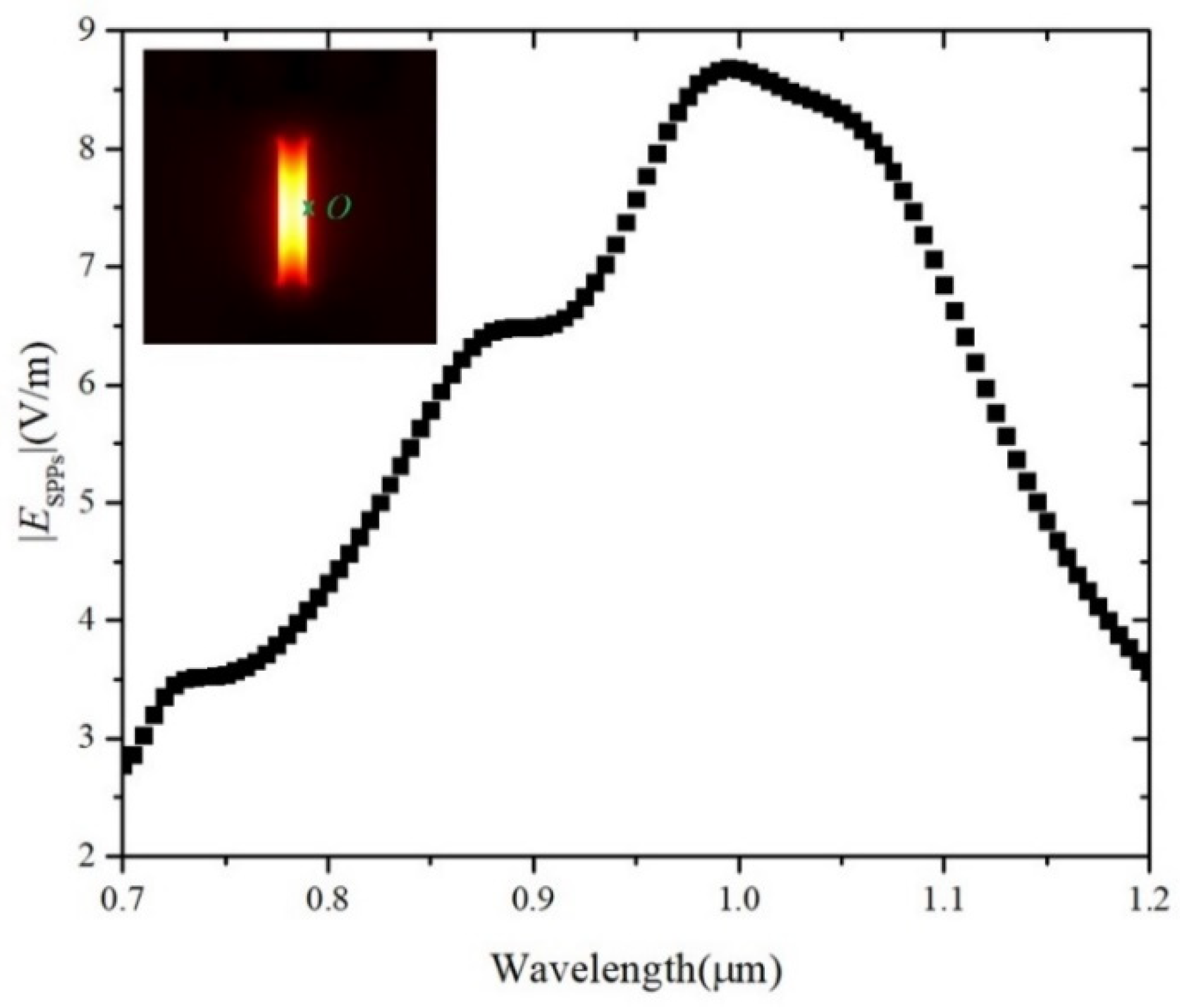
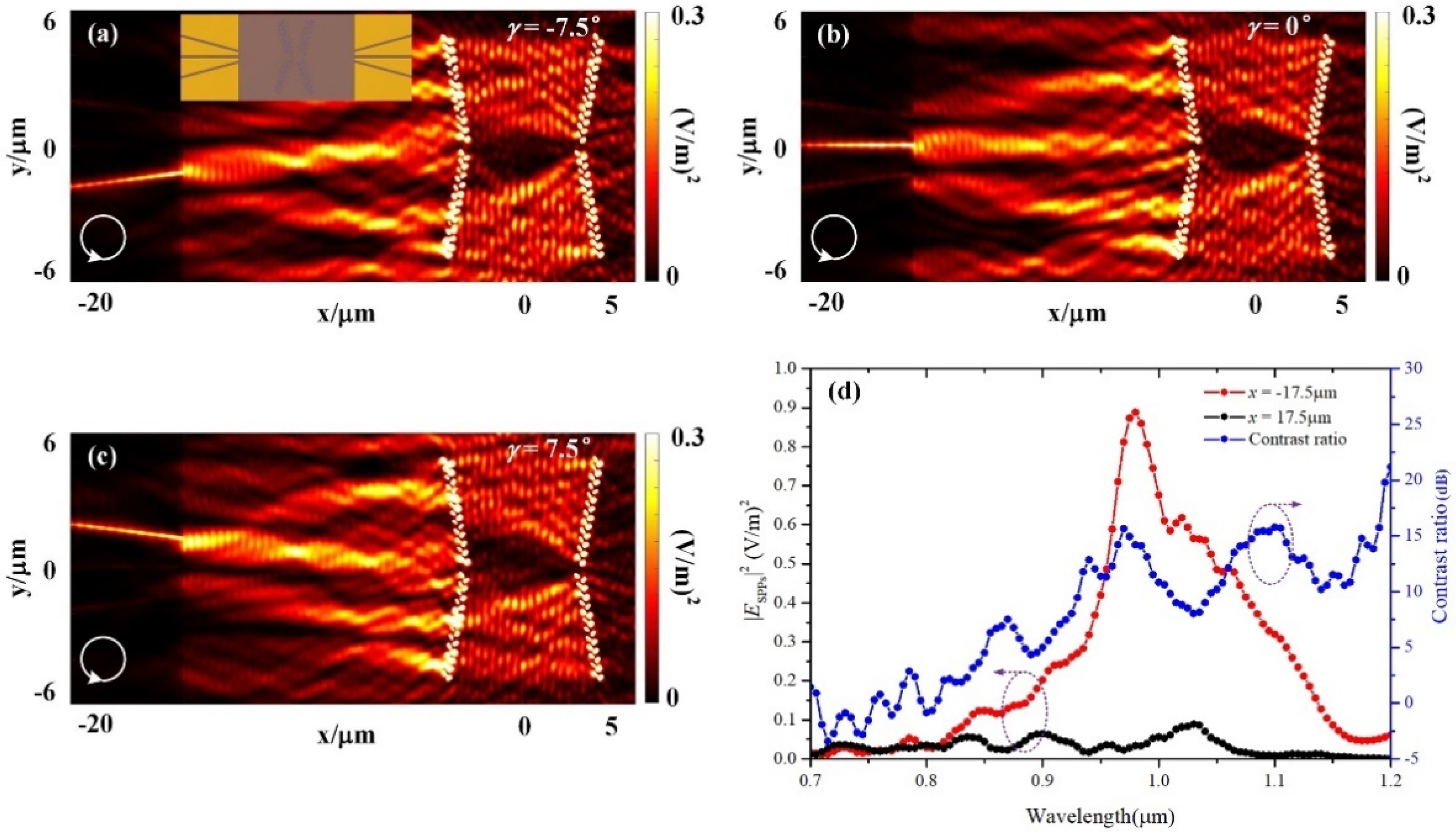
4. Simulation of Practical Spin Routing Device

In this section, we demonstrate an application example of routing optical signals to single or multiple subwavelength waveguides using nondiffracting SPP-beam launching. For this, we added a PMMA film with 250 nm thickness to the original metal/dielectric interface. In addition, we chose the communication wavelength window at 980 nm as the working wavelength to design the geometric parameters. First, we changed the structure parameters of the single nano-slot to realize the highest SPP excitation efficiency at an incident wavelength of 980 nm. The optimized width and length of the single nano-slot was chosen to be 40 and 220 nm, respectively. In the optimization, we set h = 120 nm and the refractive index of the PMMA to be 1.49. The simulated relationship between the excitation efficiency and the incident wavelength under these parameters is shown in Figure 9. In the simulation, the incident wavelength ranged from 0.7 to 1.2 mm and the electric field polarization direction is perpendicular to the long side of the nano-slot. The SPP intensity at the point O located on the center point of the nano-slot edge was chosen to evaluate the excitation efficiency. The simulation result shows that the structural parameters can meet our requirement; thus, we used the nano-slot with these geometric parameters to design practical spin-routing devices.
For incident light of 980 nm, the dielectric constant of the gold is −39.938 + 2.75855i, so the wavelength of the SPPs is 967.65 nm. We hence set S = 242 nm and D = 400   nm in our design. To connect the routing device to the second-order on-chip photonic functional element, we designed strip waveguides to transmit the SPP signal. The detailed device arrangement is shown in the inset of Figure 10a. The brown area presents the PMMA and the orange area presents the gold film. The strip waveguides with width of 150 nm and thickness of 250 nm were fabricated on the gold film. In order to couple the nondiffracting SPP beam to different waveguides under the different incidence angles and provide high coupling efficiency between the strip waveguides and the nondiffracting SPPs beam, the strip waveguides have the same slant angle as the nondiffracting SPP beams’ propagation directions. Therefore, we can realize on-chip nondiffracting signal routing by controlling the incidence inclined angle and the spin state. We demonstrated this by FDTD simulation. In the simulation, we designed three strip PMMA waveguides which can couple the nondiffracting signal with the inclined incidence angles of −7.5°, 0°, and 7.5°; the distance between the two subarrays on the different sides of y-axis is δ = 5 μm; and every column has 12 nano-rectangular slots. The lengths of the three strip PMMA waveguides are all 5 μm in the horizontal direction. Due to the significantly different transmission losses of the SPPs between metal/air and metal/PMMA interfaces, the nondiffracting SPP signal can only enable stable transmission in the PMMA strip waveguides, which can be seen in Figure 10a–c. Therefore, there is high coupling efficiency between the strip PMMA waveguides and the nondiffracting SPP signals. Moreover, the nondiffracting SPPS beams excited by different inclined angles will couple to different PMMA strip waveguides. In this way, we realized a dynamic tunable on-chip photonic routing device.
Considering that the wavelength will affect the spin sensitivity of the device, which may eventually lead to a failed identification of the input polarization state, we chose the center points of the two horizontal waveguides at the two sides of the aperture structure, i.e., the points (−17.5 μm, 0.09 μm) and (17.5 μm, 0.09 μm), to observe the spin sensitivity of this device in the wavelength range of 700 to 1200 nm. We used the SPP intensity contrast ratio of the two points as the evaluation criterion. Figure 10d shows the SPP intensity contrast ratio of the two points under LCP incident light in the wavelength range of 700 to 1200 nm, in which the red and black lines represent the SPP intensity at the points (−17.5 μm, 0.09 μm) and (17.5 μm, 0.09 μm) respectively, and the blue line represents the SPP intensity contrast ratio of the two points. It can be seen that the SPP intensity at the point (17.5 μm, 0.09 μm) is always very low, and the SPP intensity at the point (−17.5 μm, 0.09 μm) has a peak with a half height width of about 120 nm (950 to 1070 nm). In this wavelength range, the SPP intensity contrast ratio is larger than 8 dB. This means that the designed device has a wide working bandwidth.
Similarly, we designed a three-channel routing device, which can be used for spin-controlled multicasting. The structure of the strip PMMA waveguides is illustrated in the inset of Figure 11a. Figure 11a shows the coupling of three nondiffracting SPP beams to the three PMMA waveguides when the inclined incidence angle is 0°. In the simulation, the distance between the two subarrays on the different sides of the y-axis is δ = 1 μm, every column has 20 nano-rectangular slots, and the other parameters are the same as those used in Figure 9 and Figure 10. It can be seen that the signal transmitted by the middle PMMA strip waveguide is the strongest because the intensity of the nondiffracting SPP beam of the main lobe is larger than that of the side lobes. All the three strip PMMA waveguides can receive nondiffracting SPP signals correctly and have high coupling efficiency. We also tested the working bandwidth of this multichannel photon router. Similar to Figure 10d, we used the SPP intensity contrast ratio of the center points of one waveguide and its symmetrical waveguide at the other side of the aperture structure as the evaluation criterion. The relationship between the intensity contrast ratios of the three pairs of waveguides and the incident wavelength are shown in Figure 11b–d, respectively. It can be seen that at the center point of the left-hand side middle waveguide, i.e., (−15.5 μm, 0.09 μm), the SPP intensity has a peak with a half height width of about 140 nm (935 to 1075 nm), within which the SPP intensity contrast ratio of the point (−15.5 μm, 0.09 μm) and its symmetrical point (15.5 μm, 0.09 μm) is larger than 9 dB. At the center points of the left-hand side upper and lower waveguides, i.e., (−15.5 μm, 4.6 μm) and (−15.5 μm, −4.5 μm), the SPP intensity has a peak with a half height width of about 55 nm, within which the SPP intensity contrast ratio of these points and their symmetrical points on the right-hand side is larger than 6.5 dB.

5. Conclusions

In conclusion, a novel photon spin routing device with a simple structure was proposed. It has good anti-interference ability and dynamic tunability because it is based on nondiffracting surface plasmon beam launching and the launching direction of the nondiffracting SPP beam can be dynamically rotated to couple to different output waveguides by changing the incident angle. For the single non-diffracting SPP-beam directional launching device, the SPP beam can reconstruct itself after passing through an obstacle, and the transmission distance is larger than 20 mm. Moreover, the device also has a good broadband response. The simulation results show that the SPP intensity contrast ratio is larger than 8 dB between 950 and 1070 nm. For the multi-nondiffracting SPP-beam launching device, the non-diffracting transmission distance is larger than 15 mm. The SPP intensity contrast ratio of the main lobe is larger than 9 dB within 140 nm (935 to 1075 nm), and the SPP intensity contrast ratio of the side lobe is larger than 6.5 dB within 50 nm (930 to 980 nm) broadband. These results may be useful for practical on-chip photon spin routing and spin-controlled multicasting.

Author Contributions

Conceptualization, Z.Q., H.L.; investigation, Z.Q., H.L.; writing—original draft preparation, Z.Q., H.L.; writing—review and editing, H.L., L.Y.; funding acquisition, H.L., L.Y. All authors have read and agreed to the published version of the manuscript.

Funding

This work was supported by the National Key Research and Development Program of China (Grant No. 2019YFB2203903), the National Natural Science Foundations of China (Grant No. 62065006), the Natural Science Foundation of Guangxi (Grants No. 2019GXNSFAA245024 and No. 2020GXNSFBA159059), the Science and Technology Project of Guangxi (Grant No. AD19245064), Guangxi Key Laboratory Project of Optoelectronic Information Processing (Grant No. GD20103), and Guangxi Key Laboratory Project of Automatic Detection Technology and Instrument (Grant No. YQ20103).

Institutional Review Board Statement

Not applicable.

Informed Consent Statement

Not applicable.

Conflicts of Interest

The authors declare no conflict of interest.

References

  1. Kim, S.-J.; Yun, H.; Park, K.; Hong, J.; Yun, J.-G.; Lee, K.; Kim, J.; Jeong, S.J.; Mun, S.-E.; Sung, J.; et al. Active directional switching of surface plasmon polaritons using a phase transition material. Sci. Rep. 2017, 7, 43723. [Google Scholar] [CrossRef] [Green Version]
  2. Yang, Z.; Fu, Y.; Yang, J.; Hu, C.; Zhang, J. Spin-encoded subwavelength all-optical logic gates based on single-element optical slot nanoantennas. Nanoscale 2018, 10, 4523–4527. [Google Scholar] [CrossRef] [PubMed]
  3. Fu, Y.; Hu, X.; Lu, C.; Yue, S.; Yang, H.; Gong, Q. All-Optical Logic Gates Based on Nanoscale Plasmonic Slot Waveguides. Nano Lett. 2012, 12, 5784–5790. [Google Scholar] [CrossRef]
  4. Feng, F.; Si, G.; Min, C.; Yuan, X.; Somekh, M. On-chip plasmonic spin-Hall nanograting for simultaneously detecting phase and polarization singularities. Light. Sci. Appl. 2020, 9, 95. [Google Scholar] [CrossRef] [PubMed]
  5. Chen, J.; Chen, X.; Li, T.; Zhu, S. On-Chip Detection of Orbital Angular Momentum Beam by Plasmonic Nanogratings. Laser Photon- Rev. 2018, 12. [Google Scholar] [CrossRef]
  6. Kim, H.; Park, J.; Cho, S.-W.; Lee, S.-Y.; Kang, M.; Lee, B. Synthesis and Dynamic Switching of Surface Plasmon Vortices with Plasmonic Vortex Lens. Nano Lett. 2010, 10, 529–536. [Google Scholar] [CrossRef]
  7. Yang, S.; Chen, W.; Nelson, R.L.; Zhan, Q. Miniature circular polarization analyzer with spiral plasmonic lens. Opt. Lett. 2009, 34, 3047–3049. [Google Scholar] [CrossRef]
  8. Moon, S.-W.; Jeong, H.-D.; Lee, S.; Lee, B.; Ryu, Y.-S.; Lee, S.-Y. Compensation of spin-orbit interaction using the geometric phase of distributed nanoslits for polarization-independent plasmonic vortex generation. Opt. Express 2019, 27, 19119–19129. [Google Scholar] [CrossRef]
  9. Tanemura, T.; Balram, K.C.; Ly-Gagnon, D.-S.; Wahl, P.; White, J.S.; Brongersma, M.L.; Miller, D.A.B. Multiple-Wavelength Focusing of Surface Plasmons with a Nonperiodic Nanoslit Coupler. Nano Lett. 2011, 11, 2693–2698. [Google Scholar] [CrossRef]
  10. Liu, H.; Deng, H.; Deng, S.; Teng, C.; Chen, M.; Yuan, L. Vortex Beam Encoded All-Optical Logic Gates Based on Nano-Ring Plasmonic Antennas. Nanomaterials 2019, 9, 1649. [Google Scholar] [CrossRef] [Green Version]
  11. Zhao, H.; Zhang, J.; Liu, G.; Tansu, N. Surface plasmon dispersion engineering via double-metallic Au/Ag layers for III-nitride based light-emitting diodes. Appl. Phys. Lett. 2011, 98, 151115. [Google Scholar] [CrossRef] [Green Version]
  12. Yuan, G.H.; Wang, Q.; Tan, P.S.; Lin, J.; Yuan, X.-C. A dynamic plasmonic manipulation technique assisted by phase modulation of an incident optical vortex beam. Nanotechnology 2012, 23, 385204. [Google Scholar] [CrossRef] [PubMed]
  13. Tan, Q.; Xu, Z.; Zhang, D.H.; Yu, T.; Zhang, S.; Luo, Y. Polarization-Controlled Plasmonic Structured Illumination. Nano Lett. 2020, 20, 2602–2608. [Google Scholar] [CrossRef]
  14. Zang, X.; Mao, C.; Guo, X.; You, G.; Yang, H.; Chen, L.; Zhu, Y.; Zhuang, S. Polarization-controlled terahertz super-focusing. Appl. Phys. Lett. 2018, 113, 071102. [Google Scholar] [CrossRef]
  15. Wang, S.; Wang, X.; Kan, Q.; Qu, S.; Zhang, Y. Circular polarization analyzer with polarization tunable focusing of surface plasmon polaritons. Appl. Phys. Lett. 2015, 107, 243504. [Google Scholar] [CrossRef]
  16. Lin, J.; Mueller, J.P.B.; Wang, Q.; Yuan, G.; Antoniou, N.; Yuan, X.-C.; Capasso, F. Polarization-Controlled Tunable Directional Coupling of Surface Plasmon Polaritons. Science 2013, 340, 331–334. [Google Scholar] [CrossRef]
  17. Yang, J.; Xiao, X.; Hu, C.; Zhang, W.; Zhou, S.; Zhang, J. Broadband Surface Plasmon Polariton Directional Coupling via Asymmetric Optical Slot Nanoantenna Pair. Nano Lett. 2014, 14, 704–709. [Google Scholar] [CrossRef] [PubMed]
  18. Yao, W.; Liu, S.; Liao, H.; Li, Z.; Sun, C.; Chen, J.; Gong, Q. Efficient directional excitation of surface plasmons by a sin-gle-element nanoantenna. Nano Lett. 2015, 15, 3115–3121. [Google Scholar] [CrossRef]
  19. Guo, Q.; Zhang, C.; Hu, X. A spiral plasmonic lens with directional excitation of surface plasmons. Sci. Rep. 2016, 6, 32345. [Google Scholar] [CrossRef] [Green Version]
  20. Gao, Z.; Gao, F.; Zhang, B. Multi-directional plasmonic surface-wave splitters with full bandwidth isolation. Appl. Phys. Lett. 2016, 108, 111107. [Google Scholar] [CrossRef]
  21. Thomaschewski, M.; Yang, Y.; Wolff, C.; Roberts, A.S.; Bozhevolnyi, S.I. On-Chip Detection of Optical Spin–Orbit Interactions in Plasmonic Nanocircuits. Nano Lett. 2019, 19, 1166–1171. [Google Scholar] [CrossRef]
  22. Krauss, E.; Razinskas, G.; Köck, D.; Grossmann, S.; Hecht, B. Reversible Mapping and Sorting the Spin of Photons on the Nanoscale: A Spin-Optical Nanodevice. Nano Lett. 2019, 19, 3364–3369. [Google Scholar] [CrossRef]
  23. Kruk, S.S.; Decker, M.; Staude, I.; Schlecht, S.; Greppmair, M.; Neshev, D.N.; Kivshar, Y.S. Spin-Polarized Photon Emission by Resonant Multipolar Nanoantennas. ACS Photon- 2014, 1, 1218–1223. [Google Scholar] [CrossRef]
  24. Garcia-Ortiz, C.E.; Coello, V.; Han, Z.; Bozhevolnyi, S.I. Generation of diffraction-free plasmonic beams with one-dimensional Bessel profiles. Opt. Lett. 2013, 38, 905–907. [Google Scholar] [CrossRef] [Green Version]
  25. Wang, S.; Wang, S.; Zhang, Y. Polarization-based dynamic manipulation of Bessel-like surface plasmon polaritons beam. Opt. Express 2018, 26, 5461–5468. [Google Scholar] [CrossRef] [PubMed]
  26. Qiu, P.; Lv, T.; Zhang, Y.; Yu, B.; Lian, J.; Jing, M.; Zhang, D. Polarization Controllable Device for Simultaneous Generation of Surface Plasmon Polariton Bessel-Like Beams and Bottle Beams. Nanomaterials 2018, 8, 975. [Google Scholar] [CrossRef] [PubMed] [Green Version]
  27. Hu, Y.; Fu, S.; Yin, H.; Li, Z.; Li, Z.; Chen, Z. Subwavelength generation of nondiffracting structured light beams. Optica 2020, 7. [Google Scholar] [CrossRef]
  28. Fan, Y.; Cluzel, B.; Petit, M.; Le Roux, X.; Lupu, A.; De Lustrac, A. 2D Waveguided Bessel Beam Generated Using Integrated Metasurface-Based Plasmonic Axicon. ACS Appl. Mater. Interfaces 2020, 12, 21114–21119. [Google Scholar] [CrossRef] [PubMed]
  29. Kildishev, A.V.; Boltasseva, A.; Shalaev, V.M. Planar Photonics with Metasurfaces. Science 2013, 339, 1232009. [Google Scholar] [CrossRef] [Green Version]
  30. Jiao, L.; Jean, D.; Patrice, G.; Benoit, C.; de Frederique, F.; Federico, C. Cosine-Gauss plasmon beam: A localized long-rang non-diffracting surface wave. Phys. Rev. Lett. 2012, 9, 109. [Google Scholar]
  31. Liu, Z.; Steele, J.M.; Lee, H.; Zhang, X. Tuning the focus of a plasmonic lens by the incident angle. Appl. Phys. Lett. 2006, 88, 171108. [Google Scholar] [CrossRef] [Green Version]
  32. Egorov, D.; Dennis, B.S.; Blumberg, G.; Haftel, M.I. Two-dimensional control of surface plasmons and directional beaming from arrays of subwavelength apertures. Phys. Rev. B 2004, 70, 033404. [Google Scholar] [CrossRef] [Green Version]
Figure 1. (a) The schematic diagram of tunable and spin-controlled nondiffracting SPP-beam directional launching device, in which a nano-rectangular slot array structure is etched on a gold film. (b) The schematic diagram of the rectangle slot array and its parameters. The width and length of the nano-rectangular slot are W and L.
Applsci 11 10643 g001
Figure 2. (a,b) The nondiffracting SPP-beam intensity distribution of a single-aperture array and two-aperture array when the incident light is LCP. (c) The transversal electric field intensity distributions at x = ± 13   μ m for the incident polarization are LCP and RCP. (d) The intensity distribution of the nondiffracting SPP beam in the case that there exists a cylinder obstacle.
Applsci 11 10643 g002
Figure 3. The vector relationship of the kin and the nondiffracting SPP-beam launching direction (the inset shows the incident light direction). The line segments OP and OQ, respectively, are the equiphase lines of the SPP beams excited by the upper and lower nano-rectangular slot arrays when γ = 0 ; the line segments O P and O Q , respectively, are the equiphase lines of the SPP beams excited by the upper and lower nano-rectangular slot arrays when γ 0 ; OF is the nondiffracting SPPs beam launching direction when γ = 0 ; and O F is the nondiffracting SPP-beam launching direction when γ 0 .
Applsci 11 10643 g003
Figure 4. (a,b) The nondiffracting SPP-beam intensity distribution under inclined angle γ = 5 ° when the incident light is LCP and RCP, respectively. (c,d) The nondiffracting SPP-beam intensity distribution under inclined angle γ = 5 ° when the incident light is LCP and RCP, respectively.
Applsci 11 10643 g004
Figure 5. (a): The transversal electric field intensity distributions at x = ± 13   μ m . The blue and orange lines correspond to the conditions in which the inclined angle is −5° under different polarization states; the green and purple lines correspond to the conditions in which the inclined angle is 5° under different polarization states. (b) The intensity distribution of the nondiffracting SPP beam in the case in which a cylinder obstacle exists.
Applsci 11 10643 g005
Figure 6. (a) Three-channel nondiffracting SPP-beam intensity distribution when the incident is RCP light with inclined angle 0°. (b) The transversal electric field intensity distributions at x = ± 11 μ m . The blue and orange lines correspond to the inclined angle of −5° under different polarization states; the green and purple lines correspond to the inclined angle of 5° under different polarization states. (cf) Three-channel nondiffracting SPP-beam intensity distribution under different incident light polarization states and different inclined angles.
Applsci 11 10643 g006
Figure 7. The intensity distribution of nondiffracting SPP beams when there is a cylinder obstacle on the SPP beam’s transmission path. (a,c) The self-healing ability of the side lobe SPP beam. (b) The self-healing ability of the main lobe SPP beam.
Applsci 11 10643 g007
Figure 8. (a) The SPP intensity contrast ratio between the points (−11 μm, 0) and (11 μm, 0) under LCP incident light in the wavelength range of 500 to 1000 nm. (b) The SPP intensity distribution on the metal/air interface under LCP incident light when the wavelength is 565 nm. (c) The SPP intensity distribution on the metal/air interface under LCP incident light when the wavelength is 875 nm.
Applsci 11 10643 g008
Figure 9. The relationship between the SPP electric field intensity at point O and the incident wavelength.
Applsci 11 10643 g009
Figure 10. (ac) The coupling effect of a single nondiffracting SPP beam to different PMMA SPP waveguides when the inclined incidence angle is −7.5°, 0°, and 7.5°, respectively. The inset in (a) is the structure scheme of the spin router. (d) The relationship between the incident wavelength and the SPP intensity at points (−17.5 μm, 0.09 μm) and (17.5 μm, 0.09 μm), in addition to their contrast ratio under LCP incident light.
Applsci 11 10643 g010
Figure 11. (a) The coupling effect of three nondiffracting SPP beams to three PMMA SPP waveguides when the inclined incidence angle is 0°. The inset in (a) is the structure scheme of the routing device. (b) The SPP intensity contrast ratio between the points (−15.5 μm, 4.6 μm) and (15.5 μm, 4.6 μm) in the incident wavelength range of 700 to 1200 nm. (c) The SPP intensity contrast ratio between the points (−15.5 μm, 0.09 μm) and (15.5 μm, 0.09 μm) in the incident wavelength range of 700 to 1200 nm. (d) The SPP intensity contrast ratio between the points (−15.5 μm, −4.5 μm) and (15.5 μm, −4.5 μm) in the incident wavelength range of 700 to 1200 nm. The red and black lines represent the SPP intensity, and the blue line represents the SPP intensity contrast ratio.
Applsci 11 10643 g011
Publisher’s Note: MDPI stays neutral with regard to jurisdictional claims in published maps and institutional affiliations.

