Abstract
This paper presents an overview of emerging memory technologies. It begins with the presentation of stand-alone and embedded memory technology evolution, since the appearance of Flash memory in the 1980s. Then, the progress of emerging memory technologies (based on filamentary, phase change, magnetic, and ferroelectric mechanisms) is presented with a review of the major demonstrations in the literature. The potential of these technologies for storage applications addressing various markets and products is discussed. Finally, we discuss how the rise of artificial intelligence and bio-inspired circuits offers an opportunity for emerging memory technology and shifts the application from pure data storage to storage and computing tasks, and also enlarges the range of required specifications at the device level due to the exponential number of new systems and architectures.
1. Introduction
In the digital era, we are living through societal changes, carried by major technological revolutions. The amount of generated data is exponentially growing; in 2025, about 175 million terabytes will be generated, which would represent 10 times the volume produced in 2015 [1]. This trend comes with a large increase in connected objects and smart components and with the development of required data centers to cover the needs of social networks, streaming, and video on demand. Indeed, it is forecasted that in 2025 data centers will consume about 5% of the globe’s produced energy [2], which will cause further issues. Moreover, we are living a change of paradigm where computing system energy consumption is limited more by data transfer than computation itself, leading to the rise of memory-centric and in-memory computing systems. In this context, pressure is exerted on the memory component to fulfill the new specifications of these emerging computing system architectures.
Figure 1 presents a brief summary of the main milestones of nonvolatile memory history.
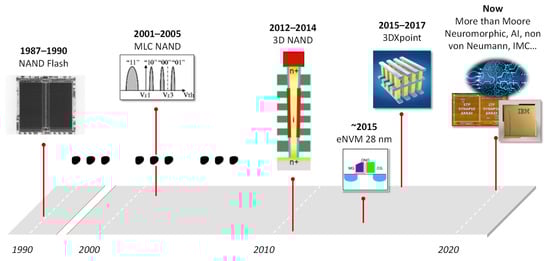
Figure 1.
Main milestones in the history of nonvolatile memories.
The history of semiconductor memory began in 1984 when Dr. Masuoka invented the NAND flash memory [3], leading to success in 1989, when Toshiba’s first NAND flash reached the market [4]. NAND technology was scaled for decades, retaining the same concept, stack, and architecture, with the memory density increasing exponentially over time [5]. In 2001, various Flash players announced and launched MLC (multilevel cell) NAND, enabling a capacity increase [6].
In 2007, Toshiba presented the first NAND integrated into 3D architecture [7], while Samsung announced in 2012 the first generation of 3D NAND.
After 2010, embedded memories began to reach the 28-nm node [8], where traditional memory cell concepts became limited in terms of area shrinkage capability and increasing complexity. Then, pressure was exerted on emerging memory concepts in order to pursue scaling to more aggressive technology nodes, opening the path to new class of embedded technologies.
In 2015, Intel and Micron developed the 3D XPoint Technology based on a phase change memory (PCM). This new class of memory enabled filling the latency gap between DRAM and Flash, often referred to as storage class memory. This made possible new system memory architectures with improved performances, bringing innovation to the nonvolatile memory (NVM) arena. The first announcement was made in 2015, and the technology has been available on the open market under the brand name Optane (Intel) since 2017 [9].
We are now in the more than Moore era, and we work toward new systems (including in-memory computing and non von Neumann architectures) that emulate the human brain to achieve high energy efficiency, parallelism, and ability in cognitive tasks, such as object recognition, association, adaptation, and learning [10]. This offers a strong opportunity for new memory technologies.
This article presents the evolution of memory technologies since the invention of Flash memory, and describes how the exponential increase in new systems (essentially coming from in-memory computing architectures, artificial intelligence, and neuromorphic circuits) offers opportunities to back-end emerging memory technologies. Section 2 presents the memory technologies’ market and trends for both stand-alone and embedded sectors. Section 3 presents an overview of emerging memories with key demonstrators presented in the literature. Finally, Section 4 analyzes how emerging memories can be used in new computing systems, for both von Neumann and non von Neumann architectures.
2. Market and Trends of Memory Technologies
2.1. Technology Trends of Nonvolatile Memories
2.1.1. Nonvolatile Memory Market
The impressive growth of the NVM market was made possible by the advent of flash memories, NOR first and NAND later, and has been fueled by the development of battery-supplied wearable electronics [11]. Thus, successive memory revolutions were supported by a novel application that allowed the market to exponentially increase. Mobile phones, PDAs, MP3 players, and digital cameras were the drivers in the 1990s [11]. With the emergence of smartphones, tablets, USB drives, and SSD (solid state drives), a new driving force led to a NAND market increase in the digital era of the 2000s [12]. More recently, artificial intelligence and other new applications offer a strong opportunity for emerging memories using new switching mechanisms. The next 10 years are expected to provide many growth opportunities for the semiconductor industry, with a continuous increase in technical and business challenges. In 2026, the NAND Flash market is predicted to represent the current GDP of medium-sized countries. Competitive pressures within many segments of the semiconductor industry will increase significantly in the future, but semiconductor companies that have innovative businesses as well as product strategies are expected to achieve financial success [13].
The memory market can be divided into two categories, high capacity standalone memories and embedded memories where the memory device is integrated into a core CMOS process flow. These two technologies are presented and described in the following sections.
2.1.2. Evolution of Standalone Nonvolatile Memory Technologies
Today, the Flash memory market is driven by high capacity standalone memories for mass storage applications. High memory capacity is required by applications such as digital still and video cameras, mp3 players, solid state drives (flash), mobile phones, and all manner of flash card products. For standalone applications, where density is doubling every 12 months [14], cell area is the key factor. Indeed, standalone memories need aggressive cell dimensions to achieve high memory densities with low cost per bit, required in the applications mentioned above.
For over 40 years, the evolution of nonvolatile memories was mostly based on the floating gate MOS transistor [1]. Scaling of the NAND technology was pursued below the 20-nm node [15]. Then, critical limits led to the appearance of 3D memory [16] that entered the market in ~2015 and changed the conservative memory world. In 2020, vertical NAND stacked up to 96 layers, used QLC (quad level cells, four bits per cells) and reached a density of about 10 Gb/mm², with typical memory capacities of one terabyte [17]. In 21 years, multilevel cell flash memory density has increased 10,000 times.
Flash NAND has been adopted in solid state drives (SSD) over the past 10 years and now shares the data storage market with hard disk drives (HDD) thanks to its constant decreasing bit cost. Three-dimensional NAND continues to improve and is expected to continue as a leading technology for data storage [1]. In the case of 3D NAND, scaling is mainly achieved by stacking, making it possible to retain the same cell dimensions in some successive nodes to maintain cell characteristics. Despite many challenges, Flash continues with constant technology, performance, architecture, and design improvements. In particular, in order to pursue scaling, stacking of two arrays (to relax the aspect ratio), integrating the CMOS under the memory array (to increase density), and adopting a more aggressive multilevel (with optimized programming algorithms) [18] with 96 stacked levels. A state-of-the-art multistacked memory hole process was presented by Toshiba in 2018 [19].
2.1.3. Trends in Embedded Nonvolatile Memory Technologies
Although the majority of the market is represented by high-density standalone memories, the embedded nonvolatile memory market is finding increasing use in a wide array of integrated circuits with applications ranging from a few bits (analog trimming) to megabytes for data/code storage. In systems with embedded nonvolatile memories, the memory array occupies only a certain fraction of the total die area due to the relatively small number of embedded bit cells. For this reason, the cell size shrink is not essential and larger cell sizes can be adopted with respect to standalone memories [20]. However, high programming voltages can lead to the need of high voltage transistors in the periphery what can impact the circuit size.
Three sectors can be distinguished for embedded memories, which are key enablers of today’s wide variety of microcontroller products [21]:
- -
- Automotive microcontrollers: these represent the most important market. The main applications include powertrain, body and convenience, safety, connectivity, security, etc.
- -
- Smartcard microcontrollers: these represent a wide range of applications, including ticketing, authentication, government ID, payment, security, etc. This market has recently increased with the rise of the Internet of Things (IoT) and connected objects.
- -
- Consumer and industrial: these also represent a wide range of applications, and include any type of machine or equipment that can use memory.
Smaller than the standalone memories market, the embedded market still represents tens of billion dollars every year with huge volume growth. Embedded specifications depend on the market and applications [22]. The most stringent market is the automotive, with aggressive specifications especially for grade 0 (−40 °C to +150 °C ambient operating temperature range).
In terms of technology, each competitor develops and uses its own memory cell concept. They all rely on charge trapping mechanisms (in a poly-Si floating gate or in a nitride charge trapping layer) and differ in cell architecture, from 1 T (one transistor) and 1.5 T (self-aligned control gate, select gate, and split gate, which is discussed further on) to 2 T options (separated select gate and memory gate). Production is currently at the 40 nm node, while 28 nm technologies are increasing in volume production. The current main embedded NVM charge storage-based cell concepts in production are described in [20].
2.2. General Context and Evolution of Nonvolatile Memories
2.2.1. The Era of Big Data
We are living during the big data revolution. Big data mainly affects large companies, in particular the GAFAMI (Amazon, Apple, Facebook, Google, Microsoft, and IBM), but also changes our everyday life. Big data relies on the three Vs: volume, variety, and velocity:
- -
- First, there is a tremendous volume of generated data. More than two trillion gigabytes (109 bytes) are created each day. Moreover, the evolution of data generation follows an exponential growth, and extrapolations forecast 175 ZB of data in 2025 [1], four times more than what we use today. People are forecasted to carry more than four mobile devices and 75% of the worldwide population will be connected to the network [23].
This data deluge is accompanied by a constant improvement in memory technologies, with bit density and memory capacity increasing by a factor of 1.4 every year [19]. In 2020, a 1-mm² die can integrate 10 Gb of memory capacity [19].
Another important point to mention is that this data increase will be supported by all memory types: even if SSD has the highest increase, HDD and even the tape market will also grow [24]. The IDC (International Data Corporation, global provider of intelligence, advisory services, and events for the information technology, telecommunications, and consumer technology markets) forecasts that over 22 ZB of storage capacity must ship across all media types from 2018 to 2025 to keep up with storage demands.
- -
- Apart from the high volume of data, there is also a large variety of data in various forms. It differs from application to application. Data come from photos, videos, audio recordings, email messages, documents, books, presentations, tweets, etc., and are generally unstructured.
- -
- Finally, new data are coming quickly. The data flow is the velocity vector. Every day 900 million photos are uploaded to Facebook, 500 million tweets are posted on Twitter, 0.4 million hours of video are uploaded to YouTube, and 3.5 billion searches are performed in Google [25]. On a large scale and considering all the contributions, data traffic was expected to grow by a factor of 1455 from 2018 to 2020, following an exponential evolution, as reported by IBS [26]. In particular, video is expected to maintain a growth rate of 70–80% every year for the next decade [26].
According to CISCO, data traffic is forecast to increase 2.5 times over the period 2016 to 2021 [27]. The majority of the increase in data traffic is due to the increase in video content delivery, projected to account for 82% of traffic by 2021 [27]. The devices that will thus be the major contributors are smartphones and TVs with respective data traffic percentages of 33% and 30% [28].
We are also in the era of IoT, with the exponential growth of connected objects in our everyday life. We have smartphones, smart watches, smart clothes, etc. The number of network-connected devices is increasing, from an estimated 18 billion in 2020 to 46 billion in 2030, which represents an almost 300% increase in that period, with an average compound annual growth rate (CAGR) of 9.8% [28]. The majority of this growth is related to automation network connected devices and, in particular, to IoT, which will represent about half of connected device stocks in 2030 [28].
2.2.2. Exponential Increase in Required Energy
This data deluge leads to greater energy consumption. It is forecasted that in 2025, data centers’ consumption will represent 5% of the globe’s energy production [29]. The International Energy Agency [30], “which aims to promote energy efficiency as the key to ensuring safe, reliable, affordable, and sustainable energy systems, provides technical analysis and policy guidance to its members and other governments concerning energy using equipment and systems”. In particular, in the frame of the Technology Collaboration Program (TCP), it delivers detailed reports on device usage and energy consumption in the Electronic Devices and Networks Annex (EDNA).
EDNA studies analyze energy consumption due to devices becoming connected to the network, and identify three main areas: upstream energy use of the communications, data networks, and data centers; network standby energy use of the edge equipment; and network active energy use of the edge and LAN equipment. Then, each device (TV, smart phone, tablet, etc.) has two energy consumption contributions, one coming from the device itself and one from the upstream network and data centers. Energy use will increase significantly from 75 TWh in 2010 to 220 TWh in 2030 for LAN devices. The largest increase in device energy use is due to machine-to-machine devices. The TV category exhibits the second largest increase in network-connected energy use at the device level, essentially due to video on demand. Smartphones, one of the largest contributors, use more upstream energy in comparison with their device energy [28].
2.2.3. Limitations of Computing Systems
The memory hierarchy of computing systems is organized in tiers, with CPU at the top for computing, followed by SRAM, DRAM, storage memory, and HDD/Tape at the bottom of the architecture. Each memory block of the system has greater capacity than the preceding but slower latency. Thus, there is a cost vs. performance tradeoff in memory subsystem, performance increasing as it moves closer to the processors. Then capacity increases by roughly one order in each subsequent level [31]. It is becoming more accepted by the community that the standard memory architecture (organized in a cache/memory/storage hierarchy) is no longer able to address the bottlenecks in current computing systems [32,33].
First, there is a latency gap between DRAM and NAND [32], leading to high energy consumption and long latency to move data within the system [34]. DRAM latency will be sustained and throughput will improve. On the other hand, NAND will maintain or improve performance with cost leadership. Thus, there is space for a new memory to enter the hierarchy, fill this gap between DRAM and NAND, and improve computing system performance [33]. This new class of memory is known as storage class memory (SCM). As it may be too difficult for one memory to fill the gap, two types of storage class memories can be distinguished: memory mapped and storage mapped [11]. Memory mapped SCM should combine read/write and endurance performances close to DRAM, with improved retention time (without being a true nonvolatile memory) and lower cost. Storage mapped SCM should be nonvolatile, cost much less than DRAM, and have improved performances (speed and endurance) with respect to Flash memories. In particular, the 3DXpoint using PCRAM fits well between NAND and DRAM in the computing memory hierarchy [31].
Moreover, memory performance and speed growth have not kept pace with that of processors (memory latency remains almost constant), leading to a performance gap known as the “memory wall” [35,36]. This performance gap between processor and memory is widening with technology scaling [37]. In von Neumann systems, separation of computing and memory becomes critical for performance and efficiency when data movement becomes prominent, as is the case in current system. Memory access energy costs 1–3 orders of magnitude higher than computing [38], and consumes approximately 1000 times the energy of a complex addition [36]. Currently, data movement between the main memory and conventional computation units is a major contributor to the total system energy consumption in consumer devices. For instance, it was reported that data movement accounts for 62.7% of the total energy consumed by Google consumer workloads [39]. This is why new non von Neumann architectures were proposed and developed to exploit locality and near-memory computing in order to reduce the cost and energy of data movement.
2.2.4. Development of New Computing Systems
The previous paragraphs highlighted the (1) current data exponential increase, (2) energy increase, and (3) performance limitations of current computing systems. For these reasons, new computing systems are currently being developed and used. In particular, near memory or in-memory computing are proposed to solve the memory wall and the high energy and time cost of data transfer in data centers. However, there is a tradeoff among the existing systems between flexibility and efficiency [1], and choosing the appropriate configuration for each purpose is key.
We can make the following classifications of computing systems depending on the application, in terms of increasing energy efficiency [38]:
- -
- CPU: they are fully programmable and versatile (can execute any function). There is a clear separation between logic and memory.
- -
- GPU: there is a shared memory architecture with thousands of cores; they operate with high parallel workload.
- -
- Near-memory processing: this system aims to supply high performance and high-density memories as close as possible to the processing units. They are dedicated to data-intensive computing (AI, graph processing, and optimization processing). They combine local and shared memory. They are used for cloud and edge devices.
- -
- In-memory processing: in this system, computing and memory are collocated, which eliminates the von Neumann bottleneck. Major changes in both memory and computing units must be achieved in order to couple data processing and storage. In-memory processing is used for vector processing (AI with limited model size) and is mostly used for edge devices.
- -
- Neuromorphic dynamical systems: they are brain inspired and merge logic and memory. They are used for AI or autonomous systems.
Among all these systems, there are many artificial neural networks and especially deep learning networks that have matched or surpassed human level capabilities. These “neuromorphic circuits” are the subject of interest for the scientific community.
Deep neural networks (DNNs), or large-scale layered networks of artificial neurons, have profoundly transformed the field of machine learning and represent the state-of-the-art in a variety of video, image, audio, and text processing tasks. They are already deployed in many real-world applications such as Google’s image and voice search, Apple’s Siri, Facebook’s DeepText and DeepFace, Microsoft’s Skype Translator, and many others [40]. They should also enter a wider range of applications in the future, including autonomous vehicles, education, and healthcare. The rise of neuromorphic circuits offers unique opportunities for emerging memories. Among them, two terminal back-end memories integrated in crossbar arrays could significantly improve the efficiency of deep neural networks as will be discussed in the next section.
In conclusion, these new systems, offering significant computing energy, are also very demanding in terms of high reliability memories and require new memory technologies with excellent capacity, bandwidth, and performance. Research perspectives on emerging memories for new non von Neumann systems are discussed in the next sections.
3. Overview of Emerging Memory Technologies
3.1. Emerging Memory Technologies
3.1.1. Filamentary Memory
Filamentary memories (Figure 2), also known as resistive random access memories (RRAM) are based on the reversible formation and disruption of a conductive filament in an insulator sandwiched between two metal electrodes when an electric field is applied. This electrical behavior was first reported in the 1960s [41,42] and was largely studied until the early 1980s for memory device applications. In the 2000s, new classes of RRAM appeared and the interest in this technology returned [43].
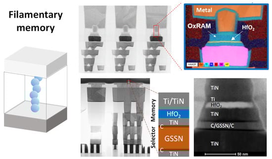
Figure 2.
TEM cross sections of an HfO2 based OxRAM integrated in the BEOL of a 28 nm FDSOI technology, from [44] (top) and an OxRAM/OTS device integrated in the BEOL of a 130 nm CMOS process, from [45] (bottom). The OTS (Ovonic Threshold Switch) backend selector is composed of a C/GeSeSbN/C stack.
Two classes of filamentary memories can be distinguished: in oxide RAM (OxRAM, the filament comes from the formation of oxygen vacancies in the resistive layer, while in CBRAM (conductive bridging RAM), it results from the dissolution of an active electrode generally made of Cu or Ag.
RRAM technology has many advantages. It is a low-cost two-terminal device and the number of integration steps is lower than in standard Flash. It also has a low voltage operation: typical RRAM operating voltages are 1–3 V, which is much lower than ~20 V of Flash NAND memories. In addition, RRAM is a fast memory, with a typical programming time of 100 ns. Less than 10 ns programming times were also reported in the literature [46].
Resistive RAM underwent a strong improvement in its performance and maturity. Demonstrations of macros are now reported down to the 22 nm node. Bitcell area of less than 0.05µm² [47] was achieved by Intel, and 20 nm cell size functionality was demonstrated by Panasonic with high performances [48]. The endurance of macros of more than one megabyte now reach 10–100 kcycles, while the intrinsic endurance was demonstrated to be more than 1010 cycles for single cells [49], showing the technology’s reliability can be further improved. In particular, Panasonic demonstrated a limited resistance distribution shift up to 100 k with 10-ppm bitcell resolution [50], and Leti showed no fail after 105 cycles on 16 kb arrays on a 28 nm node [44].
High-temperature operation is affected by oxygen vacancies (or metal) temperature assisted diffusion, limiting RRAM retention. In particular, device stability becomes critical when low programming currents are used [51]. Renesas demonstrated that it was possible to reach a −6δ margin (with a one bit ECC) after 40 min at 200 °C (equivalent to 10 years at 85 °C), which corresponds to a 0.1% chip failure of two-megabyte cells [52].
Finally, good scalability was shown: scaled memory devices include: 10 nm crossbar OxRAM [53] and 5 nm liner CBRAM [54]; further density improvements could be obtained with vertical RRAM architecture [43].
As filamentary switching can be observed in most integrated layers, many elements were investigated until some consensus finally appeared on transition metal oxides (Ta2O5, HfO2, Al2O3, etc.). Depending on the integrated materials, various device performances are possible, enabling targeting of various applications.
Today the main application of RRAM is in embedded products. For classical embedded technologies, chip cost reduction will be very difficult beyond 2× nm nodes, due to their limited scalability and increasing complexity for integration in sub−28 nm CMOS nodes [20]. For that reason, RRAM is a strong candidate for future nodes due to its simple bitcell structure and low process complexity. RRAM is highly studied for IoT for its good density and low power consumption. Panasonic proposed the first commercially available implementation of RRAM. They offered a microcontroller for portable healthcare, security equipment, or sensor processing applications. Renesas also investigated RRAM for low-power microcontroller units (MCUs) for IoT applications [52]. Intel [47,55] and TSMC [56] both demonstrated RRAM based macros in 22 nm in a 1T1R configuration for embedded applications, with comparable features (85 °C 10-year retention, 10 kcycles endurance). Intel studies mobile and RF applications and TSMC targets eFlash, IoT, and smartcards. Adesto offers RRAM based EEPROM, as a compatible serial memory for discrete and embedded memory applications. They target IoT and other energy-conscious applications. The startup Crossbar is also very active and provides RRAM for IoT system-on-chips but also persistent memory solutions.
In the case of embedded applications, the memory is integrated in the BEOL above the logic. In particular, the memory cell is integrated above the select transistor in the 1T1R configuration. The bitcell area is limited by the transistor more than by the memory itself [57]. Thus, it is important to have low operating voltages. Ideally, the RRAM would use logic transistors where the voltage was ~1 V. Due to the short RRAM programming time (~100 ns), the transistor could operate in overdrive mode [57]. This leads a targeted RRAM programming voltage of ~1.5 V to be compatible with logic CMOS to reach the best bitcell density. For more advanced nodes (1× nm nodes), the memory could be integrated in a 1S1R configuration with a backend selector [58,59] to reduce the bitcell size and target higher capacities than the 1T1R architecture allows [60].
The main issue for RRAM is the variability and related resistance distribution spread for high and low resistive states. Indeed, the conductive filament is composed with a finite number of atoms, and the memory operation is governed by stochastic phenomena [61,62]. Thus, from cycle to cycle, the conductive filament can have various shapes and is constituted by an uncontrolled number of atoms leading to resistance variability. This resistance dispersion reduces the read window margin and limits the maximum memory capacity that can be achieved. In order to improve RRAM variability, various solutions have been investigated. The first is to improve the memory stack [63,64]. In particular, “subquantum” CBRAM where filaments comprise a semiconductor or semimetal instead of a metal were proposed [65] in order to achieve thicker filaments, less affected by single events. The second approach is to adjust programming schemes and algorithms in order to reach sharper resistance distributions [66,67].
Once RRAM variability is improved, larger capacities can be envisaged and new fields can be targeted. In particular, storage class memories (SCM) can be envisaged where the RRAM would be placed between the DRAM and storage memory in the hierarchy due to its high speed and good endurance. A few years ago, Micron presented a 16 Gb RRAM in a 27 nm node targeting SCM applications with excellent reliability, achieving 105 cycles with <7 × 10⁻⁵ of bit error rate due to optimized programming schemes [68]. No further work has reported from Micron but SONY also provides cross-point RRAM for storage class memory applications with an excellent widow margin of two decades at 3δ [69]. Western Digital introduced RRAM in its roadmap [70] and announced “RRAM SCM will close the gap in terms of per-GB cost with BiCS NAND and will thus widen the gap with DRAM, which will make it more economically feasible”. RRAM also has the potential to enable analog neuromorphic computing features. This could allow low power neuromorphic IP in embedded nonvolatile memory system-on-chip without adding additional process complexity [20]. More details are provided in the next section.
In summary, RRAM is a proven technology with very low cost, ease of integration in the backend, suitable for embedded (smart card and IoT) and neuromorphic applications. Solving the variability issue would enable opening the application field to other domains such as storage class memories.
3.1.2. Phase Change Memory
Phase change memory (Figure 3) is based on the reversible transition between amorphous (insulating) and crystalline (conductive) states of a chalcogenide alloy. The phase transition is obtained by current-induced Joule heating. The most typical materials are Ge2Sb2Te5 (GST) or GeTe. Chalcogenide has been researched for a long time, and used as a recording material for optical disks, and chalcogenide memory is in the market although its density is small.
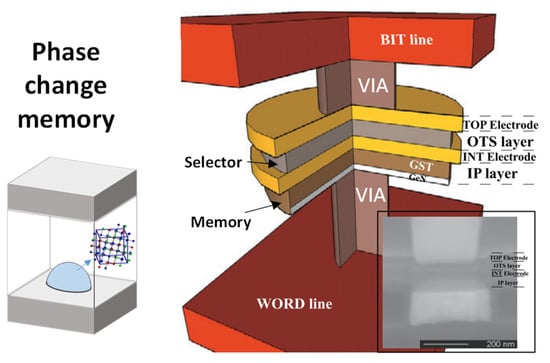
Figure 3.
3D schematics and SEM cross section of a GeSbTe (GST) phase change memory integrated with GeSeSbN OTS selector from [71].
Phase change memories offer low voltage operation (<3 V), fast behavior (~100 ns switching), and nonvolatility. Very high endurance (1012 cycles at the single cell level) has been demonstrated. It is a two terminal device and can be integrated into the BEOL. Phase change memories do not require any initialization step (unlike RRAM, for example) and work in unipolar mode. Moreover, phase change memories can have an analog behavior, which is suitable for some neuromorphic applications. The device characteristics can be tuned through material engineering (doping, etc.). Thus, they have the capability to address the high temperature retention required in embedded applications and the high speed required, for example, in storage class memory applications depending on the elected stack [72,73].
In terms of limitations, phase change memory technology suffers from resistance drift that can affect its high temperature retention [74,75]. Optimized programming schemes (better than detection threshold adjustment over time) were proposed to improve immunity to drift for multilevel operations [76]. Moreover, they generally need elevated (hundreds of µA) currents to operate (linked to the melting temperature of the material and to the current density needed to achieve such a temperature), which can be a limitation for consumption and crossbar integration. This is balanced, nevertheless, by the fact that the programming current decreases as the cell size is called: a 20 nm confined cell can be reset at <100 µA [77,78]. However, at high density, thermal disturbance among neighboring cells can become critical and may require additional layers. In terms of speed, quenching time can limit the programming speed. In terms of process and integration, PCRAM may also require complex alloys (ternary or quaternary materials) with an accurate control of the layer composition. They can also need specific device structures such as wall architecture to improve programming efficiency with more technological steps and lithography levels than other emerging memories.
PCRAM has a high maturity and products already use this technology. The most well-known is the 3D Crosspoint technology developed by Intel and Micron that integrates the PCRAM with a backend selector in crosspoint arrays. The technology is used as a storage class memory to fill the latency gap between DRAM and NAND in the memory hierarchy. Two types were initially envisaged with two different locations in the system [1]: “Storage mapped” is part of the memory hierarchy with typical 128 Gb memory capacities. The memory is faster than NAND, has higher endurance, and is 10X more dense than conventional memories. “Memory mapped” is a shadow of DRAM; data in DRAM are copied to the 3D XPoint in order to expand the size of the main memory. Intel has proposed Optane. Intel Optane DC Persistent and SSD/Caches memories can achieve 100s ns and 1s µs, respectively, allowing significant improvement of computer architecture [79]. Micron also offered the X100 NVMe™ SSD cache memory based on 3D XPoint™ Technology. STMicroelectronics also provides PCRAM technology for automotive embedded applications for 28 nm node and beyond [80,81]. The memory uses a chalcogenide ternary material and is integrated in the BEOL of 28 nm FDSOI technology, with a cell size of 0.036 µm². A bit error rate of <10−8 was achieved after multiple bakes at 150 °C and 10 k cycling of code storage memory was shown.
So far, phase change memory technology has followed the Gartner Hype Cycle, with R&D in the 1960s, followed by the first product generation (Samsung for mobile phones), negative press in the 2000s (reporting drift issue during retention), and a second product generation (3D-Xpoint) now in the market.
In summary, PCRAM is a mature technology showing high reliability, fast speed, and high endurance, which makes it a strong candidate for both automotive grade embedded applications and storage class memories.
3.1.3. Magnetic Memory
MRAM (magnetic RAM) is a memory that uses the magnetism of electron spin to provide non-volatility (Figure 4). MRAM stores information in magnetic material integrated with silicon circuitry.
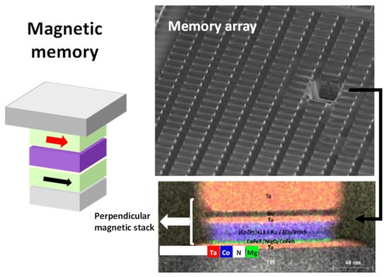
Figure 4.
TEM cross-sections of perpendicular STT-MRAM integrated in a four kilobyte array in the BEOL of a 130 nm CMOS process, from [82].
Toggle MRAM uses a one transistor, one MTJ (magnetic tunnel junction) cell to provide a simple high-density memory. During a read, the pass transistor is activated and data are read by comparing the resistance of the cell to a reference device. During writes, the magnetic field from Write Line 1 and Write Line 2 writes the cell at the intersection of the two lines but does not disturb other cells on either line. Another MRAM technology uses a spin torque transfer property, which is the manipulation of the spin of electrons with a polarizing current, to establish the desired magnetic state of the free layer to program, or write, the bits in the memory array. Spin transfer torque MRAM (STT-MRAM) provides a significant reduction in switching energy compared to toggle MRAM and is highly scalable, enabling higher density memory products.
The advantage of MRAM is fast switching speed compared to other nonvolatile memories, with ~1–10 ns read and write erase times and very good endurance (up to 1015 cycles).
One major concern with MRAM is the scalability that is difficult due to the complexity of etching many layers with good conformity. Moreover, MRAM etching generally uses ion beam etching, which is not suitable for extensive scaling. The other generally reported issue is MRAM data retention. However, recent material and stack development allowed significantly improved retention performances [83], which can be attributed to the adoption of a dual MgO interface instead of the standard single layer.
MRAM also suffers from small ON/OFF current ratio compared to the other emerging memories: STT-MRAM has a small window and TMR reduces with temperature [83,84]. Multilevel is difficult to achieve and MRAM requires a good sense amplifier. One decade ago, magnetic memories were envisaged for SRAM replacement (last level cache) due to their high speed and endurance. However, the retention and reliability of MRAM has been highly improved, opening the range of applications to eDRAM (Samsung [85]), embedded (Samsung [85], GlobalFoundries [86], Intel [87]), Industrial (Everspin [88]), and even automotive (TSMC) applications.
Intel recently presented significant improvements in MRAM technology [89,90] for embedded applications. STT-MRAM is also proposed by GF for Embedded, MCU, and IoT applications [86]. Avalanche is shipping perpendicular MRAM for SRAM (manufactured at partner foundries) but also announced the production in 2020 of a 22 nm MRAM for Flash replacement for nonvolatile embedded applications [84]. The limitation of spin memories was retention, but recent achievements by TSMC have shown that this technology can be envisaged for automotive applications in the near future [82].
Several products already exist in the market, such as the spin transfer torque MRAM for DDR3 and the DDR4 (DRAM) product of Everspin using STT-MRAM, serial peripheral interface (SPI) and parallel interface MRAM (using toggle MRAM technology) from Everspin, and the SPSRAM (a persistent SRAM using STT-MRAM technology with serial peripheral interface) and SPNOR (perpendicular STT-MRAM for embedded Flash and embedded SRAM used in system-on-chips) memories from Avalanche technology.
In summary, MRAM offers excellent endurance suitable for DRAM and SRAM applications, but has also shown recent increased stability for embedded applications. Stack complexity is generally invoked as a device limitation. The next challenge will be to increase its scalability and capacity.
3.1.4. Ferroelectric Memory
Ferroelectric memories (FeRAM) are based on the polarization of ferroelectric materials (Figure 5). In an FeRAM, thin ferroelectric films are sandwiched between two metallic electrodes and used as capacitors. When an electric field is applied across the stack, the states are aligned with the electric field leading to a low-energy state. Analogically, the high-energy state is obtained when the polarization alignment is antiparallel to the electric field. Moving from the high-energy state to the low-energy state or vice versa produces energy as a charge and is normally called a switch charge (Qs). Therefore, two Q(V) curves are obtained as a function of the polarization of the electric field applied. An access transistor is used to sense the state of the ferroelectric film, while the typical polarization depends on the electric field.
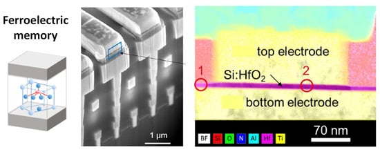
Figure 5.
SEM and TEM cross sections of ferroelectric TiN/10 nm Si (1%)-implanted HfO2/TiN capacitors integrated between M4 and M5 of a 130 nm CMOS, from [91].
Ferroelectrics are theoretically an ideal solution for low write power nonvolatile memories. However, the complexity of ferroelectric perovskites has hindered the scaling of such devices to competitive feature sizes. The discovery of ferroelectricity in hafnium oxide solved this issue, and led to renewed interest by the scientific community in this concept for various applications, due to its CMOS compatibility [92,93,94].
Three types of ferroelectric-based memories are:
- -
- Ferroelectric FET (FeFET): the ferroelectric material is embedded in the gate stack of a transistor. The nonvolatile polarization of the material acts as a remnant control gate and leads to a threshold voltage shift of the characteristics. This concept offers ultra-low power but is a three terminal device and can thus hardly be envisaged for high-density applications. Moreover, the effect vanishes for thin layers, making the concept hardly scalable. Finally, the degradation of the interface layer between the ferroelectric and the semiconductor channel limits endurance, in particular, due to trapped charge that affects the conduction of the FET below the ferroelectric [92]. For all of these reasons FeFET are targeting Flash or EEPROM rather than DRAM replacement. In particular, it is now seen as an alternative to Flash for ultra-low power applications [91], due to its 10 fJ/bit consumption and five-nanosecond programming speed. FeFET based eNVM solutions were integrated into leading edge technologies: GlobalFoundries FeFET technology was embedded into the 28 nm gate first HKMG low power CMOS platform, showing 6δ distribution, reasonable endurance, and stable data retention [95]. GF also demonstrated a 22 nm node on FDSOI CMOS technology [96].
- -
- Capacitor based ferroelectric RAM (FeRAM): in this case, the cell resembles a DRAM with the capacitor dielectric replaced by the ferroelectric. Recent reports verified antiferroelectric properties for pure ZrO2 dielectrics used in DRAM stacks. By employing electrodes with different work function values, a built-in bias is introduced within the anti-ferroelectric stack, thus creating two stable nonvolatile states [97]. It demonstrated 1010 endurance and 10 ns speed combined with 100 °C retention, making this concept very promising for a dense (6 F²) and new class of nonvolatile DRAM. In FeRAM, reading is destructive as it is performed by switching the ferroelectric into a specific direction and measuring the contrast between a switching and a nonswitching event. Thus, programming is required after each reading operation. In terms of FeRAM reliability challenges, trapped charges at the ferroelectric-electrode interface have to be controlled to improve retention (requiring careful interface engineering), while dielectric breakdown induced by high coercive film has to be prevented to insure high endurance [92].
- -
- Ferroelectric tunneling junctions (FTJ): in this case, the memory is a two terminal device. In the FTJ, a very thin ferroelectric film is used that allows tunneling and the tunneling current is modulated by the polarization of the ferroelectric. A critical issue for this concept (which is more prospective than the previous ones) is the low read current.
In summary, FeRAM is a simple and low cost memory offering very low consumption (~10 fJ/bit), suitable for low power applications (IoT, etc). Its high endurance and nonvolatility also make it a promising technology for the future, including neuromorphic circuits.
3.1.5. Emerging Memory Benchmark
A tentative benchmark is proposed in Figure 6.
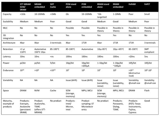
Figure 6.
Tentative benchmark of various emerging memory technologies for various applications.
In this table, two parts are reported for some technologies. Indeed, adjusting the materials and stacks, it is possible to tune the memory characteristics and target distinct applications. In particular, we consider standalone, embedded, cache, and DRAM replacement applications.
The features are questionable and can be debated; the table only gives general trends for various emerging technologies, while characteristics can vary depending on the materials and technological maturity. Nevertheless, this table can be used as a starting point to evaluate how these new technologies can solve current challenges.
Finally, Figure 7 focuses on macros for embedded applications. Most macros are integrated in 28 nm or 22 nm nodes. Cell size, limited by the selected transistor, is always in the range of 0.04–0.05 µm². The best endurance has been demonstrated for MRAM with 106 cycles (10–100 kc for Resistive RAM, 100 kc for Phase Change RAM). Various applications are targeted, from smartcard and IoT to automotive grade MCU.
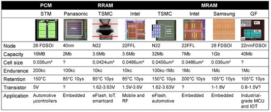
Figure 7.
Table summarizing the emerging memory macros for embedded applications.
4. New Systems with New Memories
4.1. Evolution of Von Neumann Computing Systems
Emerging memory technologies can be used in several places in this hierarchy, each having its own advantages with respect to the current implementation:
- -
- It can be used in the storage memory area, either as a replacement of current flash technology, or, at least in the short term as an intermediate step between the main memory and the flash or disks: storage class memories (SCM); in this case, the memory will be interfaced via an I/O-like interface, such as SATA, Ethernet, PCIe, or another interface that could emerge, and the transfer of data with the main memory could be managed by the OS (operating system) of the chip as it is today for storage memory. The storage memory market being essentially cost-driven, it is likely that RRAM will only replace the now well-established flash technology when it is cost-competitive; as flash density continues to increase due to monolithic 3D integration, this will take time. In the meantime, the emerging memory could be used as an intermediate step between flash and the main memory, as for instance an ultra-fast SSD used to store data with frequent access. The large difference in latency is likely to make acceptable a higher cost. Currently, the gap in latency between the main memory, which is in the order of 30–50 ns and the one of flash-based storage, which is about 100 µs (much more in writing) is vast, and having a technology enabling microsecond scale latencies would undoubtedly be an improvement for data centric applications. For these reasons, 1 µs latency and 106 cycle high density RRAM and PCRAM (possibly in vertical architectures) could be two strong candidates for this role.
- -
- It can be used in the main memory area, either as a DRAM companion chip, located on the same memory bus, or as a replacement of the DRAM. Inserting the emerging memory on the main memory bus, alongside DRAM components, will present significant system benefits. It will improve data integrity management; data can be quickly secured locally, on a word-by-word basis, instead of using current cumbersome journaling or check-pointing schemes to protect data from events such as a loss of power supply. This can significantly reduce data traffic in a data center, as it is estimated that data integrity management can represent up to 80% of the file system usage in PetaFlop data centers. As the emerging memory should become more dense and less expensive than DRAM, it will enable much greater capacity than main memories; this is especially important for big data applications, where storing large multidimensional tables in the main memory enables a tremendous performance advantage, because these tables often need to be accessed in a different order than the way it has been stored in the storage memory, which can only be accessed sequentially. It will also simplify atomic operations in transactional databases, as RRAM are byte addressable and nonvolatile. They propose a much more efficient solution than current NVDIMMs composed of a mix of DRAM and flashes powered by a bulky supercapacitor during the data transfer from DRAM to Flash when the main power supply is lost. For these reasons, according to the specifications, fast (~100 ns) and high endurance (~109 cycles) RRAM and PCRAM could succeed.
- -
- It can also be used as a last-level cache replacement or complement; it is unlikely that memory technology could become fast enough to be used as a first-level cache. In this case, the cache capacity could be made much higher, diminishing the external bandwidth requirements. Here, the most stringent requirements would be speed (<30 ns) and endurance (>1016). We cannot rely on wear-leveling in this case as the cache capacity would not be sufficient in regard to its bandwidth, each bit being written frequently. A high endurance of 1016 cycles is likely to reserve this application for STT-MRAM. FeRAM could be placed between an SCM memory (memory type) and the DRAM due to its high endurance. Finally, the only technology that exhibits performances close to SRAM is the SOT-MRAM. As far as cost and power consumption are concerned, the reference there is embedded DRAM (eDRAM); the RRAM has to be cheaper and less consuming than eDRAM to be competitive.
A summary of the possible implementation of emerging memories in the memory hierarchy is presented in Figure 8. In this figure, storage class memory refers to a class of memory that stands between DRAM and disk storage in the data storage hierarchy. In other work, this class of memory has been defined as persistent memory [98]. The difference at the system level between persistent storage, nonpersistent DRAM extension, and persistent memory at the architecture level is not discussed in this paper.
Figure 8.
Possible implementation of emerging memories in the memory hierarchy based on the benchmark presented in Figure 6.
4.2. Emerging Memories for Non Von Neumann Systems
In the context of the development of new architectures, emerging memories could enable revolutionary novel functions and computing paradigms due to their specificities (Figure 9). Thus, apart from von Neumann architecture evolutions, emerging memories offer new types of applications that can be classified as follows: novel functions, in/near memory computing, and neuromorphic architectures.
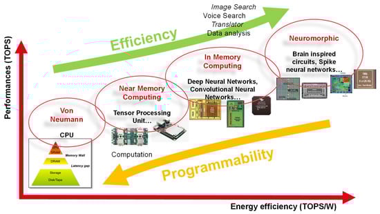
Figure 9.
Performance vs. energy efficiency in computing systems.
4.2.1. Novel Functions
A large number of work takes advantage of multiple undesirable nanoscale OxRAM phenomena, such as RESET current stochastics fluctuation, random telegraph noise (RTN), and RESET state resistance variability to realize security and computing circuits [99] such as random number generators (RNG) [100] or physical unclonable functions (PUF). However, some RRAM features do not following fully random laws: some correlation exists among subsequent RRAM levels, for instance [101], and the filament retains some memory effect of its morphology in the previous cycles [54]. Moreover, the reliability of RRAM PUF may degrade with retention loss, read instability, and thermal variation, while PUF uniqueness is maintained as long as the randomness in the RRAM resistance distribution is preserved [102]. Thus, implied physics have to be clearly understood to insure sufficient reliability of the circuit. More generally, as device physicists, our knowledge on the physics of new technologies helps us to understand how it can serve the emergence of new systems and architectures, which requires improving our knowledge on system aspects to be able to communicate with architects.
4.2.2. In/Near Memory Computing
In-memory computing uses nonvolatility and the ability to couple computing with data, such as through Ohm’s law to perform multiplication. Artificial neural networks take advantage of this by reducing the amount of data movement compared to von Neumann architectures. The expected performances strongly depend on the application and targeted system. However, general guidelines can be drawn. First, co-integration and persistence of the memory are prerequisite, while endurance and capacity are the key expected features. In order to move computing tasks in the emerging memory, endurance has to remain as close as possible to SRAM performances: the higher the endurance, the more important the amount of computing that can be done in the emerging device. Then, increasing the memory capacity will enable improving system complexity and performance. Again, the gain in memory capacity has to be significant with respect to what can be achieved with SRAM. As endurance and capacity increase, the system efficiency and performance will be improved.
Today, RRAM and PCRAM endurance is insufficient to perform computing in a device, and only specific computing tasks can be achieved with a limited number of cycles. On the contrary, MRAM appears to be a promising technology due to its excellent endurance. The challenge of this technology will be to improve its capacity, using more scalable spin-based concepts [103], in order to envisage the development of more complex and better performing systems.
Ternary content addressable memory (TCAM) can also be listed as a computing architecture. TCAM performs parallel searches by comparing input searched data with data stored in the memory and returning the data address when a match occurs. TCAMs provide a lookup response in a single clock cycle making them faster and more energy-efficient than random access memory-based search systems. Emerging memories and in particular RRAMs are a promising solution to implement TCAMs and can offer more area- and energy-efficiency with respect to static random access memory (SRAM)-based TCAMs [104].
4.2.3. Neuromorphic Architectures
As stated before, time and energy spent to move data between memory and processor (across the so-called von Neumann bottleneck) has become the main issue of computational systems, especially for datacentric applications such as realtime image recognition and natural language processing. One way to improve computing system efficiency and capabilities is to study the human brain. It is characterized by its complex parallel architecture connecting myriad low-power computing elements (neurons) and adaptive memory elements (synapses), which outperforms modern von Neumann processors on many tasks involving unstructured data classification and pattern recognition [105].
Various works report neuromorphic digital chips to improve the energy efficiency of the multiply accumulate operation, which is the basic task required in deep neural networks. Among the large number of demonstrations and approaches of proposed neuromorphic architectures, a distinction can be made between digital neural network accelerators, analog deep learning accelerators, and spiking brain inspired neural networks. In 2016, a TrueNorth brain chip was proposed and presented by IBM [106] as an energy efficient bio-inspired circuit to implement AI. This is an asynchronous parallel-distributed modular scalable architecture, and for this reason, it is considered to be non von Neumann architecture. At a prospective level, the MAC operation can be directly performed in the memory exploiting Kirchhoff’s law [107]. In this context, advanced memory devices offering high capacity, nonvolatility, and also ML and analog behavior are perfectly suited for these new architectures. More details are presented in the following for the various neuromorphic architecture categories.
- -
- Digital neural network
Research into custom digital accelerators primarily focuses on redesigning a GPU-like processor, explicitly designed for deep learning, using full ASIC designs or FPGAs.
In the approach followed by Stanford, emerging memories can be used to improve the efficiency of microcontrollers for various applications representing machine learning (including convolutional neural network). In particular, in [108] improved accuracy of neural network inference was shown with a RRAM and SRAM chip, with faster (lower latency) and lower energy features during transition to shutdown than Flash can offer. RRAM, used for inference, stores neural network model weights (five levels). During active mode, instructions are read in the RRAM and executed in the microcontroller core. After the data are processed, the results are written back to the RRAM. Instructions are read in the RRAM and executed in the µcontroller core. Thus, nonvolatile memories, and in particular, emerging backend memories become an essential on-chip device due to their fast and low energy operation, suitable for a wide range of application domains, from edge nodes for the Internet of Things (IoT) to large computing clusters.
In a digital neural network accelerator, key requirements for emerging memories would be low latency (compared to Flash), nonvolatility, limited endurance (for offline learning), and high capacity. Thus, OxRAM and PCM can be good candidates for these systems.
- -
- Analog deep learning accelerator
The core of any analog-based accelerator is a memory array that can store the values of the weight matrix in an analog fashion [105]. Analog computing is made possible with an emerging memory that exhibits an analog behavior, which is the case with PCRAM in particular, and with RRAM to a certain extent (changing the programming current or using various RESET states). This can be utilized, for example, in constructing analog circuits that solve linear systems of equations in constant rather than polynomial time. These systems can operate in a read mode, which reduces the endurance requirements of the memory. A typical example is the achievement of the multiply accumulate (MAC) operation within large memory arrays [107,109,110] as demonstrated by IBM. Multiplication between a set of input voltages and programmed conductances in an array is the dominant operation performed in modern neural networks. In IBM circuits, emerging memory is coupled to another device to perform inference and training tasks; a PCM is used for inference while training, which requires extensive endurance, and is insured by a capacitor [111] or by SRAM [112].
These innovative architectures impose constraints and requirements on the memory technologies such as very high capacity, multilevel capabilities with high accuracy on device conductance and low variability, high endurance, and low power consumption. In this context, several techniques have been proposed in the literature to solve the imperfections of current technologies: in [113], a mixed hardware–software neural-network implementation combines long-term storage in PCM (for weight data), near-linear updates of volatile capacitors, and weight-data transfer with ‘polarity inversion’ to cancel out inherent device-to-device variations. In [114,115], RRAM are used in low precision binarized neural networks (BNN), to cope with device non-idealities. In this type of neural network, both synaptic weights and neuron activations are implemented by binary values (+1 or −1) after a network training process.
Panasonic developed neuromorphic computing based on analog RRAM, resistive analog neuromorphic device (RAND), as a low power solution for edge application [116]. The authored demonstrated MNIST recognition and sensor application in which several networks could be configured at the same time.
Finally, multiple bits-per-cell was demonstrated in OxRAM in 1T4R configuration due to gradual SET/RESET [117]. The authors claim that this makes the structure suitable for multiple deep learning applications and showed high degrees of inference accuracy within 0.01% of ideal values. However, statistical cell-to-cell variability limits the maximum number of levels because of the overlap between adjacent resistance distributions [118], and OxRAM resistance relaxation after programming leads to overlap of the memory states, which can alter the circuit reliability [119].
- -
- Spiking brain inspired neural network
In spiking neural networks, the approach is to mimic human brain behavior and to represent data with spikes. Spiking neural networks (SNN) with spike-timing dependent plasticity (STDP) are then capable of replicating bio-realistic online/unsupervised learning [120,121], which is not the case for deep learning architectures relying on supervised backpropagation. In SNN processes, the simultaneous spiking activity at two neurons can lead to a potentiation of the synapse connecting them, meaning that two neurons which are active in response to the same event, should be linked by a relatively strong synaptic connection.
In this field, various demonstrations were proposed in the literature, aiming at implementing STDP in hardware synapses adopting various classes of emerging memories (including RRAM, CBRAM, STT-MRAM, and PCM). In [122], and [123] OxRAM synapses based on HfO2 and SiOx resistive memory technologies were combined with analog neurons in spiking neural networks for MNIST digit classification. The OxRAM, coding the synaptic weights of the network, was thus used for inference in the DNN, which required high reading operations but only a very limited number of cycles.
As for an analog neural network, no emerging technology can afford the high number of cycles that can offer continuous learning of the system. Thus, today, learning is performed offline, and synaptic weights are then coded in the nonvolatile memories for inference.
In conclusion, the emergence of high capacity memories, with good endurance, ideally with analogic behavior (or at least multilevel) can significantly improve the efficiency of data transfer and allow the emergence of new computing and non von Neumann systems.
5. Conclusions
The general context of nonvolatile memories is characterized by several key points. First, the era of big data in which we live implies a constant and tremendous increase in data volume generation associated with the increase in the number of connected objects. The introduction into the market of 3D-NAND allowed pursuing a density increase. At the system level, the memory hierarchy suffers from two limitations, memory wall (between SRAM and DRAM) and latency gap (between DRAM and Flash), offering opportunities for new technologies. Data deluge also changed the paradigm of computing system; limited today by data transfer more than computing. This leads to the necessity for more efficient and specialized architectures, such as in-memory computing and neuromorphic circuits.
At the component level, there is currently a renewed interest in emerging memory technologies (RRAM, PCRAM, MRAM, FeRAM, etc), based on “old” concepts due to the combination they offer in terms of fast speed, high endurance, and nonvolatility. Today, no universal memory has been discovered so far, and we move towards the co-existence of various concepts, more and more specialized to a specific application.
Currently, 3D-NAND is dominant in the world of standalone memories and there is no clear need for a new concept to replace it. However, there is an opportunity for emerging memories to enter the memory hierarchy in new (von Neumann and non von Neumann) computing systems to improve efficiency and performances. Innovation will thus consist in new architectures made possible by the advent of new memory technologies showing more and more maturity. This will require strong collaboration and mutual understanding between device engineers and system architects. On the other hand, it is more difficult and expensive to maintain current embedded charge based technologies for newtechnology nodes. Various emerging technologies are thus called upon to enter the embedded memory market. The wide range of existing applications in this domain should result in the appearance of various technologies depending on the applications. To fill these requirements, there is a place for a dedicated research to improve emerging memory performances, based on evolving concepts, new materials, and also optimized programming schemes, which should be adapted to the physics of emerging devices.
Author Contributions
Writing—original draft preparation: G.M.; Writing—review and editing: E.N. All authors have read and agreed to the published version of the manuscript.
Funding
This work has been partially supported by the European Commission, French State and Auvergne-Rhône Alpes region through the ECSEL project ANDANTE and the French Nano2022 program.
Institutional Review Board Statement
Not applicable.
Informed Consent Statement
Not applicable.
Data Availability Statement
Not applicable.
Acknowledgments
The authors would like to acknowledge L. Grenouillet, J. Minguet Lopez, L. Reganaz, P. Trotti, J. F. Nodin, G. Navarro, E. Vianello, M. Bernard, C. Sabbione, T. Magis, R. Crochemore, N. Castellani, S. Martin, V. Meli, B. Giraud, J. P. Noel, A. Valentian, F. Rummens, F. Martin, M. Harrand, C. Carabasse, A. Persico, M. C. Cyrille, E. Esmanhotto, C. Jahan, T. Hirtzlin, E. Jalaguier, C. Charpin, P. Tran, C. Cagli, G. Pillonet, S. Oukassi, T. Bauvent, J. Coignus, O. Billoint, and F. Andrieu from CEA-Leti for significant help and fruitful discussions.
Conflicts of Interest
The authors declare no conflict of interest.
References
- Ishimaru, K. Future of Non-Volatile Memory—From Storage to Computing. In Proceedings of the 2019 IEEE International Electron Devices Meeting (IEDM), San Francisco, CA, USA, 7–11 December 2019; pp. 1.3.1–1.3.6. [Google Scholar] [CrossRef]
- Data Centres of the World Will Consume 1/5 of Earth’s Power by 2025. Available online: https://data-economy.com/data-centres-world-will-consume-1-5-earths-power-2025/ (accessed on 10 December 2020).
- Masuoka, F.; Asano, M.; Iwahashi, H.; Komuro, T.; Tanaka, S. A new flash E2PROM cell using triple polysilicon technology. In Proceedings of the 1984 International Electron Devices Meeting, San Francisco, CA, USA, 9–12 December 1984; pp. 464–467. [Google Scholar] [CrossRef]
- Available online: https://spectrum.ieee.org/chip-hall-of-fame-toshiba-nand-flash-memory (accessed on 10 December 2020).
- Ogura, T. Flash Memory. In CMOS Processors and Memories. Analog Circuits and Signal Processing; Iniewski, K., Ed.; Springer: Dordrecht, The Netherlands, 2010. [Google Scholar] [CrossRef]
- Cho, T.; Lee, Y.T.; Kim, E.C.; Lee, J.W.; Choi, S.; Lee, S.; Kim, D.H.; Han, W.G.; Lim, Y.H.; Lee, D.J.; et al. A dual-mode NAND flash memory: 1-Gb multilevel and high-performance 512-Mb single-level modes. IEEE J. Solid-State Circuits 2001, 36, 1700–1706. [Google Scholar] [CrossRef]
- Tanaka, H.; Kido, M.; Yahashi, K.; Oomura, M.; Katsumata, R.; Kito, M.; Fukuzumi, Y.; Sato, M.; Nagata, Y.; Matsuoka, Y.; et al. Bit Cost Scalable Technology with Punch and Plug Process for Ultra High Density Flash Memory. In Proceedings of the 2007 IEEE Symposium on VLSI Technology, Kyoto, Japan, 12–14 June 2007; pp. 14–15. [Google Scholar] [CrossRef]
- Available online: https://www.renesas.com/us/en/about/press-room/renesas-electronics-develops-industrys-first-28nm-embedded-flash-memory-technology-microcontrollers (accessed on 10 December 2020).
- Available online: https://www.intel.com/content/www/us/en/products/details/memory-storage/optane-memory.html (accessed on 10 December 2020).
- Available online: https://www.research.ibm.com/articles/brain-chip.shtml (accessed on 10 December 2020).
- Cappelletti, P. Non volatile memory evolution and revolution. In Proceedings of the 2015 IEEE International Electron Devices Meeting (IEDM), Washington, DC, USA, 7–9 December 2015; pp. 10.1.1–10.1.4. [Google Scholar] [CrossRef]
- Aritome, S. Nand Flash Memory Devices. In NAND Flash Memory Technologies; Wiley: Hoboken, NJ, USA, 2015; pp. 37–92. ISBN 9781119132639. [Google Scholar] [CrossRef]
- Whitepaper: Semiconductor Industry from 2015 to 2025; International Business Strategies (IBS), Inc.: Los Gatos, CA, USA, 2019.
- Hwang, C. Nanotechnology enables a new memory growth model. Proc. IEEE 2003, 91, 1765–1771. [Google Scholar] [CrossRef]
- Aritome, S. NAND Flash Memory Revolution. In Proceedings of the 2016 IEEE 8th International Memory Workshop (IMW), Paris, France, 15–18 May 2016; pp. 1–4. [Google Scholar] [CrossRef]
- Fukuzumi, Y.; Katsumata, R.; Kito, M.; Kido, M.; Sato, M.; Tanaka, H.; Nagata, Y.; Matsuoka, Y.; Iwata, Y.; Aochi, H.; et al. Optimal Integration and Characteristics of Vertical Array Devices for Ultra-High Density, Bit-Cost Scalable Flash Memory. In Proceedings of the 2007 IEEE International Electron Devices Meeting, Washington, DC, USA, 10–12 December 2007; pp. 449–452. [Google Scholar] [CrossRef]
- Shibata, N.; Kanda, K.; Shimizu, T.; Nakai, J.; Nagao, O.; Kobayashi, N.; Miakashi, M.; Nagadomi, Y.; Nakano, T.; Kawabe, T.; et al. 13.1 A 1.33Tb 4-bit/Cell 3D-Flash Memory on a 96-Word-Line-Layer Technology. In Proceedings of the 2019 IEEE International Solid-State Circuits Conference—(ISSCC), San Francisco, CA, USA, 17–21 February 2019; pp. 210–212. [Google Scholar] [CrossRef]
- Kalavade, P. 4 bits/cell 96 Layer Floating Gate 3D NAND with CMOS under Array Technology and SSDs. In Proceedings of the 2020 IEEE International Memory Workshop (IMW), Dresden, Germany, 17–20 May 2020; pp. 1–4. [Google Scholar] [CrossRef]
- Inaba, S. 3D Flash Memory for Data-Intensive Applications. In Proceedings of the 2018 IEEE International Memory Workshop (IMW), Kyoto, Japan, 13–16 May 2018; pp. 1–4. [Google Scholar] [CrossRef]
- Nishi, Y.; Magyari-Kope, B. (Eds.) Chapter 4: Improving embedded Flash memory technology. In Advances in Non-volatile Memory and Storage Technology; Woodhead Publishing: Sawston, UK, 2014; p. 139. [Google Scholar]
- Strenz, R. Review and Outlook on Embedded NVM Technologies—From Evolution to Revolution. In Proceedings of the 2020 IEEE International Memory Workshop (IMW), Dresden, Germany, 17–20 May 2020; pp. 1–4. [Google Scholar] [CrossRef]
- Wang, H. Challenges in Automotive Memory Solutions. In Proceedings of the 2018 IEEE International Memory Workshop (IMW), Kyoto, Japan, 13–16 May 2018; pp. 1–7. [Google Scholar] [CrossRef]
- Reinsel, D.; Gantz, J.; Rydning, J. IDC White Paper, Data Age 2025; Seagate, 2017; Available online: https://www.import.io/wp-content/uploads/2017/04/Seagate-WP-DataAge2025-March-2017.pdf (accessed on 10 December 2020).
- Reinsel, D.; Gantz, J.; Rydning, J. IDC White Paper, Data Age 2025. In The Digitalization of the World, from Edge to Core; #US44413318; November 2018; Available online: https://www.seagate.com/files/www-content/our-story/trends/files/idc-seagate-dataage-whitepaper.pdf (accessed on 10 December 2020).
- Available online: https://www.whishworks.com/blog/big-data/understanding-the-3-vs-of-big-data-volume-velocity-and-variety (accessed on 10 December 2020).
- Impact of Ai on Electronics and Semiconductor Industries; International Business Strategies (IBS), Inc.: Los Gatos, CA, USA, 2020.
- The Zettabyte Era: Trends and Analysis. Cisco. Available online: http://www.hit.bme.hu/~jakab/edu/HTI18/Litr/Cisco_The_Zettabyte_Era_2017June__vni-hyperconnectivity-wp.pdf (accessed on 10 December 2020).
- 4E Electronics Devices and Network Annex (EDNA). Total Energy Model for Connected Devices. June 2019. Available online: https://edna.iea-4e.org/library (accessed on 10 December 2020).
- Andrae, A. Total Consumer Power Consumption Forecast. Nord. Digit. Bus. Summit. 2017. Available online: https://www.researchgate.net/publication/320225452_Total_Consumer_Power_Consumption_Forecast (accessed on 10 December 2020).
- Available online: www.iea-4e.org (accessed on 10 December 2020).
- Kau, D.; Tang, S.; Karpov, I.V.; Dodge, R.; Klehn, B.; Kalb, J.A.; Strand, J.; Diaz, A.; Leung, N.; Wu, J.; et al. A stackable cross point Phase Change Memory. In Proceedings of the 2009 IEEE International Electron Devices Meeting (IEDM), Baltimore, MD, USA, 7–9 December 2009; pp. 1–4. [Google Scholar] [CrossRef]
- Hady, F. Converging Memory and Storage. In Proceedings of the 2019 SNIA’s Persistent Memory Summit, Santa Clara, CA, USA, 24 January 2019; Available online: https://www.snia.org/sites/default/files/PM-Summit/2019/presentations/01-PMSummit19-Hady-Keynote.pdf (accessed on 10 December 2020).
- Handy, J.; Coughlin, T. The Long and Winding Road to Persistent Memories. In Proceedings of the 2018 SNIA’s Storage Developer Conference, Santa Clara, CA, USA, 24–27 September 2018; Available online: https://www.snia.org/sites/default/files/SDC/2018/presentations/PM/Handy_J_Coughlin_T_The_Long_&_Winding_Road_to_Persistent_Memories.pdf (accessed on 10 December 2020).
- Foong, A.; Hady, F. Storage as Fast as Rest of the System. In Proceedings of the 2016 IEEE 8th International Memory Workshop (IMW), Paris, France, 15–18 May 2016; pp. 1–4. [Google Scholar] [CrossRef]
- Wulf, W.A.; McKee, S. Hitting the memory wall: Implications of the obvious. ACM SIGARCH Comput. Archit. News 1995, 23, 20–24. [Google Scholar] [CrossRef]
- Mutlu, O. Processing Data Where It Makes Sense in Modern Computing Systems: Enabling In-Memory Computation. In Proceedings of the Shortcourse of 2019 International Memory Workshop, Monterey, CA, USA, 12–15 May 2019. [Google Scholar]
- Kulkarni, J.P. Circuit Technologies for Efficient In-Memory Computing. In Proceedings of the Shortcourse of 2019 International Memory Workshop, Monterey, CA, USA, 12–15 May 2019. [Google Scholar]
- Raychowdhury, A. Towards Memory-centric Autonomous Systems: A Technology and Device Perspective. In Proceedings of the IEDM 2019 Short Course 2: Technologies for Memory-Centric Computing, San Francisco, CA, USA, 7–11 December 2019. [Google Scholar]
- Boroumand, A.; Ghose, S.; Kim, Y.; Ausavarungnirun, R.; Shiu, E.; Thakur, R.; Kim, D.; Kuusela, A.; Knies, A.; Ranganathan, P.; et al. Google Workloads for Consumer Devices: Mitigating Data Movement Bottlenecks. In Proceedings of the 23rd International Conference on Architectural Support for Programming Languages and Operating Systems (ASPLOS), Williamsburg, VA, USA, 24–28 March 2018. [Google Scholar]
- Venkataramani, S.; Ranjan, A.; Banerjee, S.; Das, D.; Avancha, S.; Jagannathan, A.; Durg, A.; Nagaraj, D.; Kaul, B.; Dubay, P.; et al. SCALEDEEP: A scalable compute architecture for learning and evaluating deep networks. In Proceedings of the 2017 ACM/IEEE 44th Annual International Symposium on Computer Architecture (ISCA), Toronto, ON, Canada, 24–28 June 2017; pp. 13–26. [Google Scholar] [CrossRef]
- Nielsen, P.H.; Bashara, N.M. The reversible voltage-induced initial resistance in the negative resistance sandwich structure. IEEE Trans. Electron Devices 1964, 11, 243–244. [Google Scholar] [CrossRef]
- Hickmott, T.W. Low-Frequency Negative Resistance in Thin Anodic Oxide Films. J. Appl. Phys. 1962, 33, 2669–2682. [Google Scholar] [CrossRef]
- Baek, I.G.; Lee, M.S.; Seo, S.; Lee, M.J.; Seo, D.H.; Suh, D.-S.; Park, J.C.; Park, S.O.; Kim, H.S.; Yoo, I.K.; et al. Highly scalable nonvolatile resistive memory using simple binary oxide driven by asymmetric unipolar voltage pulses. IEDM Technical Digest. In Proceedings of the IEEE International Electron Devices Meeting 2004, San Francisco, CA, USA, 13–15 December 2004; pp. 587–590. [Google Scholar] [CrossRef]
- Grenouillet, L.; Castellani, N.; Persico, A.; Meli, V.; Martin, S.; Billoint, O.; Segaud, R.; Bernasconi, S.; Pellissier, C.; Jahan, C.; et al. 16kbit 1T1R OxRAM arrays embedded in 28nm FDSOI technology demonstrating low BER, high endurance, and compatibility with core logic transistors. In Proceedings of the 2021 IEEE International Memory Workshop (IMW), Dresden, Germany, 16–19 May 2021; pp. 1–4. [Google Scholar] [CrossRef]
- Lopez, J.M.; Castellani, N.; Grenouillet, L.; Reganaz, L.; Navarro, G.; Bernard, M.; Carabasse, C.; Magis, T.; Deleruyelle, D.; Bocquet, M.; et al. Ge-Se-Sb-N-based OTS scaling perspectives for high-density 1 S1R crossbar arrays. In Proceedings of the 2021 IEEE International Memory Workshop (IMW), Dresden, Germany, 16–19 May 2021; pp. 1–4. [Google Scholar] [CrossRef]
- Wang, C.; Wu, H.; Gao, B.; Wu, W.; Dai, L.; Li, X.; Qian, H. Ultrafast RESET Analysis of HfOx-Based RRAM by Sub-Nanosecond Pulses. Adv. Electron. Mater. 2017, 3, 1700263. [Google Scholar] [CrossRef]
- Golonzka, O.; Arslan, U.; Bai, P.; Bohr, M.; Baykan, O.; Chang, Y.; Chaudhari, A.; Chen, A.; Clarke, J.; Connor, C.; et al. Non-Volatile RRAM Embedded into 22FFL FinFET Technology. In Proceedings of the 2019 Symposium on VLSI Technology, Kyoto, Japan, 9–14 June 2019; pp. T230–T231. [Google Scholar] [CrossRef]
- Hayakawa, Y.; Himeno, A.; Yasuhara, R.; Boullart, W.; Vecchio, E.; Vandeweyer, T.; Witters, T.; Crotti, D.; Jurczak, M.; Fujii, S.; et al. Highly reliable TaOx ReRAM with centralized filament for 28-nm embedded application. In Proceedings of the 2015 Symposium on VLSI Technology (VLSI Technology), Kyoto, Japan, 16–18 June 2015; pp. T14–T15. [Google Scholar] [CrossRef]
- Hirtzlin, T.; Bocquet, M.; Ernoult, M.; Klein, J.O.; Nowak, E.; Vianello, E.; Portal, J.-M.; Querlioz, D. Hybrid Analog-Digital Learning with Differential RRAM Synapses. In Proceedings of the 2019 IEEE International Electron Devices Meeting (IEDM), San Francisco, CA, USA, 7–11 December 2019; pp. 22.6.1–22.6.4. [Google Scholar] [CrossRef] [Green Version]
- Ito, S.; Hayakawa, Y.; Wei, Z.; Muraoka, S.; Kawashima, K.; Kotani, H.; Kouno, K.; Nakamura, M.; Du, G.A.; Chen, J.F.; et al. ReRAM Technologies for Embedded Memory and Further Applications. In Proceedings of the 2018 IEEE International Memory Workshop (IMW), Kyoto, Japan, 13–16 May 2018; pp. 1–4. [Google Scholar] [CrossRef]
- Guy, J.; Molas, G.; Cagli, C.; Bernard, M.; Roule, A.; Carabasse, C.; Toffoli, A.; Clermidy, F.; de Salvo, B.; Perniola, L. Guidance to reliability improvement in CBRAM using advanced KMC modelling. In Proceedings of the 2017 IEEE International Reliability Physics Symposium (IRPS), Monterey, CA, USA, 2–6 April 2017; pp. PM-2.1–PM-2.5. [Google Scholar] [CrossRef]
- Ueki, M.; Takeuchi, K.; Yamamoto, T.; Tanabe, A.; Ikarashi, N.; Saitoh, M.; Nagumo, T.; Sunamura, H.; Narihiro, M.; Uejima, K.; et al. Low-power embedded ReRAM technology for IoT applications. In Proceedings of the 2015 Symposium on VLSI Technology (VLSI Technology), Kyoto, Japan, 16–18 June 2015; pp. T108–T109. [Google Scholar] [CrossRef]
- Govoreanu, B.; Kar, G.S.; Chen, Y.; Paraschiv, V.; Kubicek, S.; Fantini, A.; Radu, I.P.; Goux, L.; Clima, S.; Degraeve, R.; et al. 10 × 10 nm2 Hf/HfOx crossbar resistive RAM with excellent performance, reliability and low-energy operation. In Proceedings of the 2011 International Electron Devices Meeting, Washington, DC, USA, 5–7 December 2011; pp. 31.6.1–31.6.4. [Google Scholar] [CrossRef]
- Guy, J.; Molas, G.; Blaise, P.; Carabasse, C.; Bernard, M.; Roule, A.; le Carval, G.; Sousa, V.; Grampeix, H.; Delaye, V.; et al. Experimental and theoretical understanding of Forming, SET and RESET operations in Conductive Bridge RAM (CBRAM) for memory stack optimization. In Proceedings of the 2014 IEEE International Electron Devices Meeting, San Francisco, CA, USA, 15–17 December 2014; pp. 6.5.1–6.5.4. [Google Scholar] [CrossRef]
- Jain, P.; Arslan, U.; Sekhar, M.; Lin, B.C.; Wei, L.; Sahu, T.; Alzate-vinasco, J.; Vangapaty, A.; Meterelliyoz, M.; Strutt, N.; et al. 13.2 A 3.6 Mb 10.1 Mb/mm2 Embedded Non-Volatile ReRAM Macro in 22 nm FinFET Technology with Adaptive Forming/Set/Reset Schemes Yielding Down to 0.5 V with Sensing Time of 5 ns at 0.7 V. In Proceedings of the 2019 IEEE International Solid-State Circuits Conference—(ISSCC), San Francisco, CA, USA, 17–21 February 2019; pp. 212–214. [Google Scholar] [CrossRef]
- Chou, C.; Lin, Z.; Lai, C.; Su, C.; Tseng, P.; Chen, W.; Tsai, W.; Chu, W.; Ong, T.; Chuang, H.; et al. A 22nm 96KX144 RRAM Macro with a Self-Tracking Reference and a Low Ripple Charge Pump to Achieve a Configurable Read Window and a Wide Operating Voltage Range. In Proceedings of the 2020 IEEE Symposium on VLSI Circuits, Honolulu, HI, USA, 16–19 June 2020; pp. 1–2. [Google Scholar] [CrossRef]
- Sandrini, J.; Grenouillet, L.; Meli, V.; Castellani, N.; Hammad, I.; Bernasconi, S.; Aussenac, F.; van Duijn, S.; Audoit, G.; Barlas, M.; et al. OxRAM for embedded solutions on advanced node: Scaling perspectives considering statistical reliability and design constraints. In Proceedings of the 2019 IEEE International Electron Devices Meeting (IEDM), San Francisco, CA, USA, 7–11 December 2019; pp. 30.5.1–30.5.4. [Google Scholar] [CrossRef]
- Lopez, J.M.; Robayo, D.A.; Grenouillet, L.; Carabasse, C.; Navarro, G.; Fournel, R.; Sabbione, C.; Bernard, M.; Billoint, O.; Cagli, C.; et al. Optimization of RRAM and OTS selector for advanced low voltage CMOS compatibility. In Proceedings of the 2020 IEEE International Memory Workshop (IMW), Dresden, Germany, 17–20 May 2020; pp. 1–4. [Google Scholar] [CrossRef]
- Robayo, D.A.; Sassine, G.; Lopez, J.M.; Grenouillet, L.; Verdy, A.; Navarro, G.; Bernard, M.; Esmanhotto, E.; Carabasse, C.; Deleruyelle, D.; et al. Reliability and Variability of 1S1R OxRAM-OTS for High Density Crossbar Integration. In Proceedings of the 2019 IEEE International Electron Devices Meeting (IEDM), San Francisco, CA, USA, 7–11 December 2019; pp. 35.3.1–35.3.4. [Google Scholar] [CrossRef]
- Molas, G.; Robayo, D.A.; Lopez, J.M.; Grenouillet, L.; Carabasse, C.; Navarro, G.; Sabbione, C.; Bernard, M.; Cagli, C.; Castellani, N.; et al. Crosspoint Memory Arrays: Principle, Strengths and Challenges. In Proceedings of the 2020 IEEE International Memory Workshop (IMW), Dresden, Germany, 17–20 May 2020; pp. 1–4. [Google Scholar] [CrossRef]
- Padovani, A.; Larcher, L.; Pirrotta, O.; Vandelli, L.; Bersuker, G. Microscopic Modeling of HfOx RRAM Operations: From Forming to Switching. IEEE Trans. Electron Devices 2015, 62, 1998–2006. [Google Scholar] [CrossRef]
- Guy, J.; Molas, G.; Blaise, P.; Bernard, M.; Roule, A.; Le Carval, G.; Delaye, V.; Toffoli, A.; Ghibaudo, G.; Clermidy, F.; et al. Investigation of Forming, SET, and Data Retention of Conductive-Bridge Random-Access Memory for Stack Optimization. IEEE Trans. Electron Devices 2015, 62, 3482–3489. [Google Scholar] [CrossRef]
- Sassine, G.; Nail, C.; Blaise, P.; Sklenard, B.; Bernard, M.; Gassilloud, R.; Marty, A.; Veillerot, M.; Vallée, C.; Nowak, E.; et al. Hybrid-RRAM Towards Next Generation of Non-volatile Memory: Coupling of Oxygen Vacancies and Metal Ions. Adv. Electron. Mater. 2018, 5, 1800658. [Google Scholar] [CrossRef]
- Bricalli, A.; Ambrosi, E.; Laudato, M.; Maestro, M.; Rodriguez, R.; Ielmini, D. SiOx-based resistive switching memory (RRAM) for crossbar storage/select elements with high on/off ratio. In Proceedings of the 2016 IEEE International Electron Devices Meeting (IEDM), San Francisco, CA, USA, 3–7 December 2016; pp. 4.3.1–4.3.4. [Google Scholar] [CrossRef]
- Gonzales, N.; Dinh, J.; Lewis, D.; Gilbert, N.; Pedersen, B.; Kamalanathan, D.; Jameson, J.R.; Hollmer, S. An Ultra Low-Power Non-Volatile Memory Design Enabled by Subquantum Conductive-Bridge RAM. In Proceedings of the 2016 IEEE 8th International Memory Workshop (IMW), Paris, France, 15–18 May 2016; pp. 1–4. [Google Scholar] [CrossRef]
- Sassine, G.; Cagli, C.; Nodin, J.; Molas, G.; Nowak, E. Novel Computing Method for Short Programming Time and Low Energy Consumption in HfO2 Based RRAM Arrays. IEEE J. Electron Devices Soc. 2018, 6, 696–702. [Google Scholar] [CrossRef]
- Molas, G.; Sassine, G.; Nail, C.; Robayo, D.A.; Nodin, J.; Cagli, C.; Coignus, J.; Blaise, P.; Nowak, E. (Invited) Resistive Memories (RRAM) Variability: Challenges and Solutions. ECS Trans. 2018, 86, 35. [Google Scholar] [CrossRef]
- Sills, S.; Yasuda, S.; Calderoni, A.; Cardon, C.; Strand, J.; Aratani, K.; Ramaswamy, N. Challenges for high-density 16Gb ReRAM with 27nm technology. In Proceedings of the 2015 Symposium on VLSI Technology (VLSI Technology), Kyoto, Japan, 16–18 June 2015; pp. T106–T107. [Google Scholar] [CrossRef]
- Ohba, K.; Yasuda, S.; Mizuguchi, T.; Sei, H.; Tsushima, T.; Shimuta, M.; Shiimoto, T.; Yamamoto, T.; Sone, T.; Nonoguchi, S. Cross Point Cu-ReRAM with BC-Doped Selector. In Proceedings of the 2018 IEEE International Memory Workshop (IMW), Kyoto, Japan, 13–16 May 2018; pp. 1–3. [Google Scholar] [CrossRef]
- Available online: https://www.flashmemorysummit.com/English/Collaterals/Proceedings/2016/20160809_Keynote4_WD_Sivaram.pdf (accessed on 10 December 2020).
- Navarro, G.; Verdy, A.; Castellani, N.; Bourgeois, G.; Sousa, V.; Molas, G.; Bernard, M.; Sabbione, C.; Noé, P.; Garrione, J. Innovative PCM+OTS device with high sub-threshold non-linearity for non-switching reading operations and higher endurance performance. In Proceedings of the 2017 Symposium on VLSI Technology, Kyoto, Japan, 5–8 June 2017; pp. T94–T95. [Google Scholar] [CrossRef]
- Cheng, H.Y.; Wu, J.Y.; Cheek, R.; Raoux, S.; BrightSky, M.; Garbin, D.; Kim, S.; Hsu, T.H.; Zhu, Y.; Lai, E.K.; et al. A thermally robust phase change memory by engineering the Ge/N concentration in (Ge, N)xSbyTe z phase change material. In Proceedings of the 2012 International Electron Devices Meeting, San Francisco, CA, USA, 10–13 December 2012; pp. 31.1.1–31.1.4. [Google Scholar] [CrossRef]
- Navarro, G.; Bourgeois, G.; Kluge, J.; Serra, A.L.; Verdy, A.; Garrione, J.; Cyrille, M.; Bernier, N.; Jannaud, A.; Sabbione, C. Phase-Change Memory: Performance, Roles and Challenges. In Proceedings of the 2018 IEEE International Memory Workshop (IMW), Kyoto Japan, 13–16 May 2018; pp. 1–4. [Google Scholar] [CrossRef] [Green Version]
- Li, J.; Luan, B.; Lam, C. Resistance drift in phase change memory. In Proceedings of the 2012 IEEE International Reliability Physics Symposium (IRPS), Anaheim, CA, USA, 15–19 April 2012; pp. 6C.1.1–6C.1.6. [Google Scholar] [CrossRef]
- Elliott, S.R. Electronic mechanism for resistance drift in phase-change memory materials: Link to persistent photoconductivity. J. Phys. D Appl. Phys. 2020, 53, 214002. [Google Scholar] [CrossRef]
- Stanisavljevic, M.; Pozidis, H.; Athmanathan, A.; Papandreou, N.; Mittelholzer, T.; Eleftheriou, E. Demonstration of Reliable Triple-Level-Cell (TLC) Phase-Change Memory. In Proceedings of the 2016 IEEE 8th International Memory Workshop (IMW), Paris, France, 15–18 May 2016; pp. 1–4. [Google Scholar] [CrossRef]
- Kang, M.J.; Park, T.J.; Kwon, Y.W.; Ahn, D.H.; Kang, Y.S.; Jeong, H.; Ahn, S.J.; Song, Y.J.; Kim, B.C.; Nam, S.W.; et al. PRAM cell technology and characterization in 20nm node size. In Proceedings of the 2011 International Electron Devices Meeting, Washington, DC, USA, 5–7 December 2011; pp. 3.1.1–3.1.4. [Google Scholar] [CrossRef]
- Close, G.F.; Frey, U.; Morrish, J.; Jordan, R.; Lewis, S.C.; Maffitt, T.; BrightSky, M.J.; Hagleitner, C.; Lam, C.H.; Eleftheriou, E. A 256-Mcell Phase-Change Memory Chip Operating at 2+ Bit/Cell. IEEE Trans. Circuits Syst. I Regul. Pap. 2013, 60, 1521–1533. [Google Scholar] [CrossRef]
- Pangal, K. Emerging Memories including Cross-Point: Opportunities and Challenges. In Proceedings of the IEEE IEDM 2017 Shortcourse, San Francisco, CA, USA, 2 December 2018. [Google Scholar]
- Arnaud, F.; Zuliani, P.; Reynard, J.P.; Gandolfo, A.; Disegni, F.; Mattavelli, P.; Gomiero, E.; Samanni, G.; Jahan, C.; Berthelon, R.; et al. Truly Innovative 28nm FDSOI Technology for Automotive Micro-Controller Applications embedding 16MB Phase Change Memory. In Proceedings of the 2018 IEEE International Electron Devices Meeting (IEDM), San Francisco, CA, USA, 1–5 December 2018; pp. 18.4.1–18.4.4. [Google Scholar] [CrossRef]
- Arnaud, F.; Haendler, S.; Clerc, S.; Ranica, R.; Gandolfo, A.; Weber, O. 28 nm FDSOI Platform with Embedded PCM for IoT, ULP, Digital, Analog, Automotive and others Applications. In Proceedings of the ESSCIRC 2019—IEEE 45th European Solid State Circuits Conference (ESSCIRC), Cracow, Poland, 23–26 September 2019; pp. 7–10. [Google Scholar] [CrossRef]
- Tillie, L.; Nowak, E.; Sousa, R.C.; Cyrille, M.-C.; Delaet, B.; Magis, T.; Persico, A.; Langer, J.; Ocker, B.; Prejbeanu, I.-L.; et al. Data retention extraction methodology for perpendicular STT-MRAM. In Proceedings of the 2016 IEEE International Electron Devices Meeting (IEDM), San Francisco, CA, USA, 3–7 December 2016; pp. 27.3.1–27.3.4. [Google Scholar] [CrossRef]
- Gallagher, W.J.; Chien, E.; Chiang, T.; Huang, J.; Shih, M.; Wang, C.Y.; Weng, C.; Chen, S.; Bair, C.; Lee, G.; et al. 22 nm STT-MRAM for Reflow and Automotive Uses with High Yield, Reliability, and Magnetic Immunity and with Performance and Shielding Options. In Proceedings of the 2019 IEEE International Electron Devices Meeting (IEDM), San Francisco, CA, USA, 7–11 December 2019; pp. 2.7.1–2.7.4. [Google Scholar] [CrossRef]
- Wang, Z.; Hao, X.; Xu, P.; Hu, L.; Jung, D.; Kim, W.; Satoh, K.; Yen, B.; Wei, Z.; Wang, L.; et al. STT-MRAM for Embedded Memory Applications. In Proceedings of the 2020 IEEE International Memory Workshop (IMW), Dresden, Germany, 17–20 May 2020; pp. 1–3. [Google Scholar] [CrossRef]
- Lee, K.; Bak, J.H.; Kim, Y.J.; Kim, C.K.; Antonyan, A.; Chang, D.H.; Hwang, S.H.; Lee, G.W.; Ji, N.Y.; Kim, W.J.; et al. 1Gbit High Density Embedded STT-MRAM in 28nm FDSOI Technology. In Proceedings of the 2019 IEEE International Electron Devices Meeting (IEDM), San Francisco, CA, USA, 7–11 December 2019; pp. 2.2.1–2.2.4. [Google Scholar] [CrossRef]
- Naik, V.B.; Lee, K.; Yamane, K.; Chao, R.; Kwon, J.; Thiyagarajah, N.; Chung, N.L.; Jang, S.H.; Behin-Aein, B.; Lim, J.H.; et al. Manufacturable 22 nm FD-SOI Embedded MRAM Technology for Industrial-grade MCU and IOT Applications. In Proceedings of the 2019 IEEE International Electron Devices Meeting (IEDM), San Francisco, CA, USA, 7–11 December 2019; pp. 2.3.1–2.3.4. [Google Scholar] [CrossRef]
- Alzate, J.G.; Arslan, U.; Bai, P.; Brockman, J.; Chen, Y.J.; Das, N.; Fischer, K.; Ghani, T.; Heil, P.; Hentges, P.; et al. 2 MB Array-Level Demonstration of STT-MRAM Process and Performance Towards L4 Cache Applications. In Proceedings of the 2019 IEEE International Electron Devices Meeting (IEDM), San Francisco, CA, USA, 7–11 December 2019; pp. 2.4.1–2.4.4. [Google Scholar] [CrossRef]
- Aggarwal, S.; Almasi, H.; DeHerrera, M.; Hughes, B.; Ikegawa, S.; Janesky, J.; Lee, H.K.; Lu, H.; Mancoff, F.B.; Nage, K.; et al. Demonstration of a Reliable 1 Gb Standalone Spin-Transfer Torque MRAM For Industrial Applications. In Proceedings of the 2019 IEEE International Electron Devices Meeting (IEDM), San Francisco, CA, USA, 7–11 December 2019; pp. 2.1.1–2.1.4. [Google Scholar] [CrossRef]
- Golonzka, O.; Alzate, J.-G.; Arslan, U.; Bohr, M.; Bai, P.; Brockman, J.; Buford, B.; Connor, C.; Das, N.; Doyle, B.; et al. MRAM as Embedded Non-Volatile Memory Solution for 22FFL FinFET Technology. In Proceedings of the 2018 IEEE International Electron Devices Meeting (IEDM), San Francisco, CA, USA, 1–5 December 2018; pp. 18.1.1–18.1.4. [Google Scholar] [CrossRef]
- Wei, L.; Alzate, J.G.; Arslan, U.; Brockman, J.; Das, N.; Fischer, K.; Ghani, T.; Golonzka, O.; Hentges, P.; Jahan, R.; et al. 13.3 A 7Mb STT-MRAM in 22FFL FinFET Technology with 4ns Read Sensing Time at 0.9V Using Write-Verify-Write Scheme and Offset-Cancellation Sensing Technique. In Proceedings of the 2019 IEEE International Solid- State Circuits Conference—(ISSCC), San Francisco, CA, USA, 17–21 February 2019; pp. 214–216. [Google Scholar] [CrossRef]
- Grenouillet, L.; Francois, T.; Coignus, J.; Kerdilès, S.; Vaxelaire, N.; Carabasse, C.; Mehmood, F.; Chevalliez, S.; Pellissier, C.; Triozon, F.; et al. Nanosecond Laser Anneal (NLA) for Si-Implanted HfO2 Ferroelectric Memories Integrated in Back-End of Line (BEOL). In Proceedings of the 2020 IEEE Symposium on VLSI Technology, Honolulu, HI, USA, 16–19 June 2020; pp. 1–2. [Google Scholar] [CrossRef]
- Mulaosmanovic, H.; Lomenzo, P.D.; Schroeder, U.; Slesazeck, S.; Mikolajick, T.; Max, B. Reliability aspects of ferroelectric hafnium oxide for application in non-volatile memories. In Proceedings of the 2021 IEEE International Reliability Physics Symposium (IRPS), Monterey, CA, USA, 21–25 March 2021; pp. 1–6. [Google Scholar] [CrossRef]
- Mikolajick, T.; Schroeder, U.; Lomenzo, P.D.; Breyer, E.T.; Mulaosmanovic, H.; Hoffmann, M.; Mittmann, T.; Mehmood, F.; Max, B.; Slesazeck, S. Next Generation Ferroelectric Memories enabled by Hafnium Oxide. In Proceedings of the 2019 IEEE International Electron Devices Meeting (IEDM), San Francisco, CA, USA, 7–11 December 2019; pp. 15.5.1–15.5.4. [Google Scholar] [CrossRef]
- Grenouillet, L.; Francois, T.; Coignus, J.; Vaxelaire, N.; Carabasse, C.; Triozon, F.; Richter, C.; Schroeder, U.; Nowak, E. Performance assessment of BEOL-integrated HfO2-based ferroelectric capacitors for FeRAM memory arrays. In Proceedings of the 2020 IEEE Silicon Nanoelectronics Workshop (SNW), Honolulu, HI, USA, 13–14 June 2020; pp. 5–6. [Google Scholar] [CrossRef]
- Beyer, S.; Dünkel, S.; Trentzsch, M.; Müller, J.; Hellmich, A.; Utess, D.; Paul, P.; Kleimeier, D.; Pellerin, J.; Müller, S.; et al. FeFET: A versatile CMOS compatible device with game-changing potential. In Proceedings of the 2020 IEEE International Memory Workshop (IMW), Dresden, Germany, 17–20 May 2020; pp. 1–4. [Google Scholar] [CrossRef]
- Dünkel, S.; Trentzsch, M.; Richter, R.; Moll, P.; Fuchs, C.; Gehring, O.; Majer, M.; Wittek, S.; Müller, B.; Melde, T.; et al. A FeFET based super-low-power ultra-fast embedded NVM technology for 22nm FDSOI and beyond. In Proceedings of the 2017 IEEE International Electron Devices Meeting (IEDM), San Francisco, CA, USA, 2–6 December 2017; pp. 19.7.1–19.7.4. [Google Scholar] [CrossRef]
- Pesic, M.; Knebel, S.; Hoffmann, M.; Richter, C.; Mikolajick, T.; Schroeder, U. How to make DRAM non-volatile? Anti-ferroelectrics: A new paradigm for universal memories. In Proceedings of the 2016 IEEE International Electron Devices Meeting (IEDM), San Francisco, CA, USA, 3–7 December 2016; pp. 11.6.1–11.6.4. [Google Scholar] [CrossRef]
- Hady, F.T.; Foong, A.; Veal, B.; Williams, D. Platform Storage Performance With 3D XPoint Technology. Proc. IEEE 2017, 105, 1822–1833. [Google Scholar] [CrossRef]
- Carboni, R.; Ielmini, D. Stochastic Memory Devices for Security and Computing. Adv. Electron. Mater. 2019, 5, 1900198. [Google Scholar] [CrossRef] [Green Version]
- Sahay, S.; Kumar, A.; Parmar, V.; Suri, M. OxRAM RNG Circuits Exploiting Multiple Undesirable Nanoscale Phenomena. IEEE Trans. Nanotechnol. 2017, 16, 560–566. [Google Scholar] [CrossRef]
- Piccolboni, G.; Molas, G.; Garbin, D.; Vianello, E.; Cueto, O.; Cagli, C.; Traore, B.; de Salvo, B.; Ghibaudo, G.; Perniola, L. Investigation of Cycle-to-Cycle Variability in HfO2-Based OxRAM. IEEE Electron Device Lett. 2016, 37, 721–723. [Google Scholar] [CrossRef]
- Chen, A. Comprehensive assessment of RRAM-based PUF for hardware security applications. In Proceedings of the 2015 IEEE International Electron Devices Meeting (IEDM), Washington, DC, USA, 7–9 December 2015; pp. 10.7.1–10.7.4. [Google Scholar] [CrossRef]
- Perrissin, N.; Gregoire, G.; Lequeux, S.; Tillie, L.; Strelkov, N.; Auffret, S.; Prejbeanu, L.D.B.; Sousa, R.C.; Vila, L.; Dieny, B.; et al. Perpendicular shape anisotropy spin transfer torque magnetic random-access memory: Towards sub-10 nm devices. J. Phys. D Appl. Phys. 2019, 52, 234001. [Google Scholar] [CrossRef]
- Ly, D.R.B.; Noel, J.P.; Giraud, B.; Royer, P.; Esmanhotto, E.; Castellani, N.; Dalgaty, T.; Nodin, J.-F.; Fenouillet-Berange, C.; Nowak, E.; et al. Novel 1T2R1T RRAM-based Ternary Content Addressable Memory for Large Scale Pattern Recognition. In Proceedings of the 2019 IEEE International Electron Devices Meeting (IEDM), San Francisco, CA, USA, 7–11 December 2019; pp. 35.5.1–35.5.4. [Google Scholar] [CrossRef]
- Tsai, H.; Ambrogio, S.; Narayanan, P.; Shelby, R.M.; Burr, G.W. Recent progress in analog memory-based accelerators for deep learning. J. Phys. D Appl. Phys. 2018, 51, 283001. [Google Scholar] [CrossRef]
- Available online: https://www.ibm.com/blogs/research/2016/12/the-brains-architecture-efficiency-on-a-chip/ (accessed on 10 December 2020).
- Ielmini, D.; Wong, H.-S.P. In-memory computing with resistive switching devices. Nat. Electron. 2018, 1, 333–343. [Google Scholar] [CrossRef]
- Wu, T.F.; Le, B.Q.; Radway, R.; Bartolo, A.; Hwang, W.; Jeong, S.; Li, H.; Tandon, P.; Vianello, E.; Vivet, P.; et al. 14.3 A 43pJ/Cycle Non-Volatile Microcontroller with 4.7μs Shutdown/Wake-up Integrating 2.3-bit/Cell Resistive RAM and Resilience Techniques. In Proceedings of the 2019 IEEE International Solid- State Circuits Conference—(ISSCC), San Francisco, CA, USA, 17–21 February 2019; pp. 226–228. [Google Scholar] [CrossRef]
- Sheng, X.; Graves, C.E.; Kumar, S.; Li, X.; Buchanan, B.; Zheng, L.; Lam, S.; Li, C.; Strachan, J.P. Low-Conductance and Multilevel CMOS-Integrated Nanoscale Oxide Memristors. Adv. Electron. Mater. 2019, 5, 1800876. [Google Scholar] [CrossRef]
- Strukov, D.; Indiveri, G.; Grollier, J.; Fusi, S. “Building brain-inspired computing. Nat. Commun. 2019, 10, 4838. [Google Scholar] [CrossRef] [Green Version]
- Burr, G.W.; Shelby, R.M.; Sebastian, A.; Kim, S.; Kim, S.; Sidler, S.; Virwani, K.; Ishii, M.; Narayanan, P.; Fumarola, A.; et al. Neuromorphic computing using non-volatile memory. Adv. Phys. X 2017, 2, 89–124. [Google Scholar] [CrossRef]
- Joshi, V.; le Gallo, M.; Haefeli, S.; Boybat, I.; Nandakumar, S.R.; Piveteau, C.; Dazzi, M.; Rajendran, B.; Sebastian, A.; Eleftheriou, E. Accurate deep neural network inference using computational phase-change memory. Nat. Commun. 2020, 11, 2473. [Google Scholar] [CrossRef]
- Ambrogio, S.; Narayanan, P.; Tsai, H.; Shelby, R.M.; Boybat, I.; di Nolfo, C.; Sidler, S.; Giordano, M.; Bodini, M.; Farinha, N.C.P.; et al. Equivalent-accuracy accelerated neural-network training using analogue memory. Nature 2018, 558, 60–67. [Google Scholar] [CrossRef] [PubMed]
- Hirtzlin, T.; Bocquet, M.; Penkovsky, B.; Klein, J.; Nowak, E.; Vianello, E.; Portal, J.; Querlioz, D. Digital Biologically Plausible Implementation of Binarized Neural Networks with Differential Halfnium Oxide Resistive Memory Arrays. Front. Neurosci. 2020, 13, 1383. [Google Scholar] [CrossRef] [PubMed] [Green Version]
- Bocquet, M.; Hirztlin, T.; Klein, J.-O.; Nowak, E.; Vianello, E.; Portal, J.-M.; Querlioz, D. In-Memory and Error-Immune Differential RRAM Implementation of Binarized Deep Neural Networks. In Proceedings of the 2018 IEEE International Electron Devices Meeting (IEDM), San Francisco, CA, USA, 1–5 December 2018. [Google Scholar] [CrossRef] [Green Version]
- Mikawa, T.; Yasuhara, R.; Katayama, K.; Kouno, K.; Ono, T.; Mochida, R.; Hayata, Y.; Nakayama, M.; Suwa, H.; Gohou, Y.; et al. Neuromorphic computing based on Analog ReRAM as low power solution for edge application. In Proceedings of the 2019 IEEE 11th International Memory Workshop (IMW), Monterey, CA, USA, 12–15 May 2019; pp. 1–4. [Google Scholar] [CrossRef]
- Hsieh, E.R.; Giordano, M.; Hodson, B.; Levy, A.; Osekowsky, S.K.; Radway, R.M.; Shih, Y.C.; Wan, W.; Wu, T.F.; Zheng, X.; et al. High-Density Multiple Bits-per-Cell 1T4R RRAM Array with Gradual SET/RESET and its Effectiveness for Deep Learning. In Proceedings of the 2019 IEEE International Electron Devices Meeting (IEDM), San Francisco, CA, USA, 7–11 December 2019; pp. 35.6.1–35.6.4. [Google Scholar] [CrossRef]
- Milo, V.; Zambelli, C.; Olivo, P.; Pérez, E.; Mahadevaiah, M.K.; Ossorio, O.G.; Wenger, C.; Ielmini, D. Multilevel HfO2-based RRAM devices for low-power neuromorphic networks. APL Mater. 2019, 7, 081120. [Google Scholar] [CrossRef] [Green Version]
- Esmanhotto, E.; Brunet, L.; Castellani, N.; Bonnet, D.; Dalgaty, T.; Grenouillet, L.; Ly, D.R.B.; Cagli, C.; Vizioz, C.; Allouti, N.; et al. High-Density 3D Monolithically Integrated Multiple 1T1R Multi-Level-Cell for Neural Networks. In Proceedings of the 2020 IEEE International Electron Devices Meeting (IEDM), San Francisco, CA, USA, 12–18 December 2020; pp. 36.5.1–36.5.4. [Google Scholar] [CrossRef]
- Maass, W. Networks of Spiking Neurons: The Third Generation of Neural Network Models. Neural Netw. 1997, 10, 1659–1671. [Google Scholar] [CrossRef]
- Ielmini, D.; Ambrogio, S. Emerging neuromorphic devices. Nanotechnology 2020, 31, 092001. [Google Scholar] [CrossRef] [PubMed]
- Valentian, A.; Rummens, F.; Vianello, E.; Mesquida, T.; Lecat-Mathieu de Boissac, C.; Bichler, O.; Reita, C. Fully Integrated Spiking Neural Network with Analog Neurons and RRAM Synapses. In Proceedings of the 2019 IEEE International Electron Devices Meeting (IEDM), San Francisco, CA, USA, 7–11 December 2019; pp. 14.3.1–14.3.4. [Google Scholar] [CrossRef]
- Regev, A.; Bricalli, A.; Piccolboni, G.; Valentian, A.; Mesquida, T.; Molas, G.; Nodin, J. Fully-Integrated Spiking Neural Network Using SiOx-Based RRAM as Synaptic Device. In Proceedings of the 2020 2nd IEEE International Conference on Artificial Intelligence Circuits and Systems (AICAS), Genova, Italy, 31 August–2 September 2020; pp. 145–148. [Google Scholar] [CrossRef]


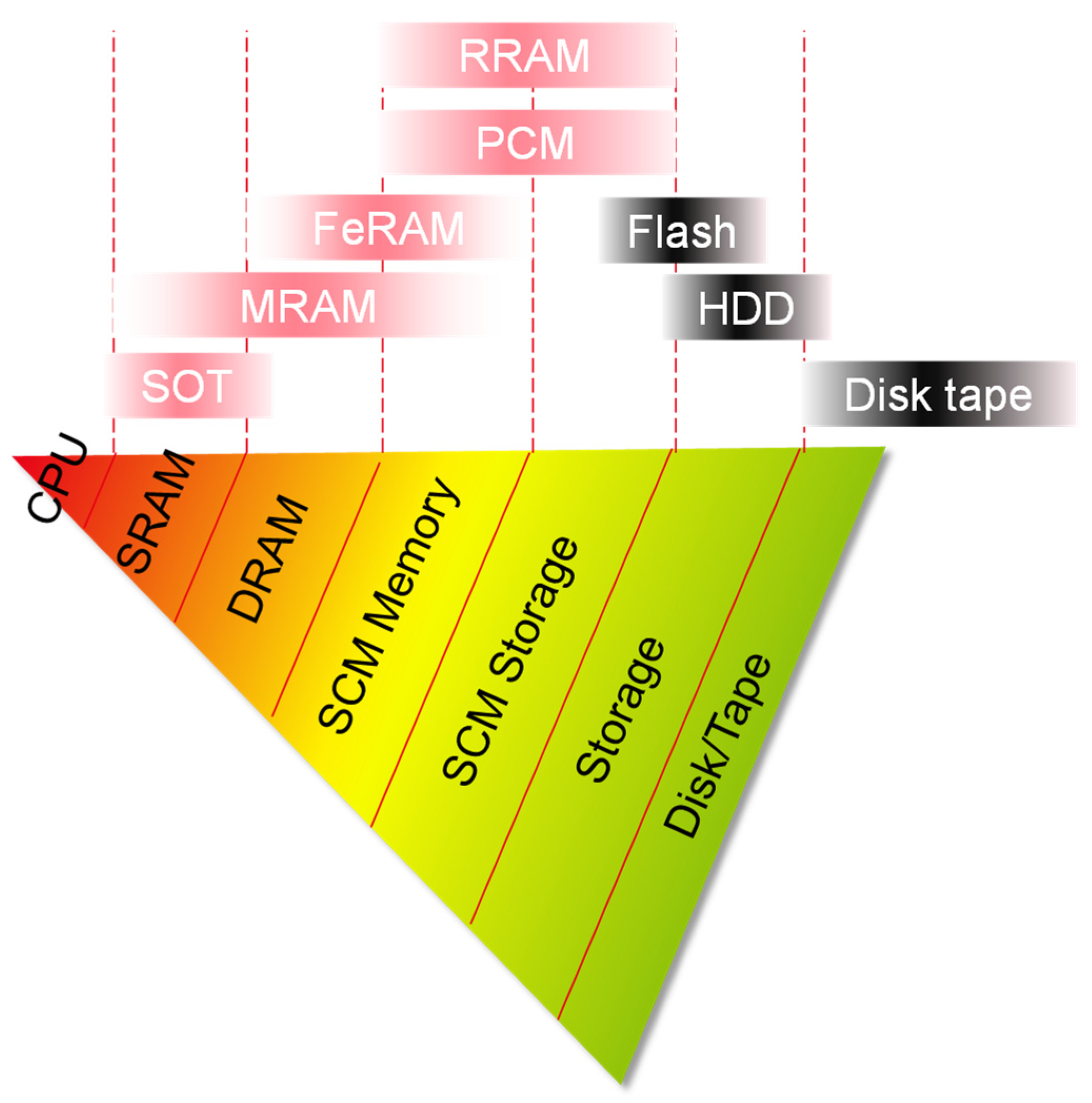

Publisher’s Note: MDPI stays neutral with regard to jurisdictional claims in published maps and institutional affiliations. |
© 2021 by the authors. Licensee MDPI, Basel, Switzerland. This article is an open access article distributed under the terms and conditions of the Creative Commons Attribution (CC BY) license (https://creativecommons.org/licenses/by/4.0/).