Article

Optimization Technique for High-Gain CMOS Power Amplifier for 5G Applications

1
School of Electronic Engineering, College of Information Technology, Soongsil University, Seoul 06978, Korea
2
Electronics and Telecommunications Research Institute (ETRI), Daejeon 34129, Korea
*
Author to whom correspondence should be addressed.
Appl. Sci. 2021, 11(24), 11691; https://doi.org/10.3390/app112411691
Submission received: 28 October 2021 / Revised: 22 November 2021 / Accepted: 6 December 2021 / Published: 9 December 2021
(This article belongs to the Section Electrical, Electronics and Communications Engineering)

Abstract

:
In this study, a differential power amplifier (PA) with a high gain of over 30 dB by configuring a three-stage common source unit amplifier was designed. To ensure the stability of the high-gain differential PA, the analysis to apply the capacitive neutralization method to the differential common source PA was conducted. From the analysis, the required neutralized capacitance was quantitatively calculated from the estimated parasitic components of a power cell used in the PA. To verify the feasibility of the proposed optimization technique, a Ka-band PA was designed with a 65 nm RFCMOS process. The measurement results showed a gain of 30.7 dB. The saturated output power was measured as 16.1 dBm, maximum power-added efficiency (PAE) was 29.7%, and P1dB was 13.1 dBm.

1. Introduction

Recently, with the adoption of fifth-generation (5G) communication standards, active research has been conducted on millimeter-wave (mm-Wave) power amplifiers (PAs); particularly, the demand for monolithic microwave integrated circuit (MMIC) operating at Ka-band frequency to satisfy the 5G standards is increasing [1,2].
More recently, studies have been underway to configure single-chip transceivers by utilizing high-integrity characteristics of CMOS [3,4,5]. However, it may not communicate smoothly if the transceiver path lacks gain, which is calculated to determine the appropriate margin when performing link budget analysis. Therefore, to compensate for the lack of gain, a gain amplifier would be required based on the IC specifications, resulting in a larger IC size and complexities. The link-budget calculations in our study show that if a single PA secures a minimum gain of 27 dB, the transceiver IC does not require additional amplifiers, and can be designed to be more marginal.
In this work, a PA capable of obtaining high gain was designed, and the problem of stability that may occur due to the high gain was solved using a neutralization capacitor. To this end, for the first time, we extracted the optimal value of the neutralization capacitor using a differential structure.

2. Design and Optimization of the Power Amplifier

Herein, we present the optimization technique and the design process of a high-gain differential PA with the capacitive neutralization method in detail. In this study, a 65 nm RFCMOS is selected to design a differential three-stage common-source PA with high gain. The target frequency bandwidth is between 26.5–29.5 GHz. with a supply voltage of 1 V. Further, a neutralized capacitor Cneu is used to improve the stability of the high-gain PA, and the capacitance required depends on the transistor size [6,7,8].
The design process described below is summarized as follows. First, the size of the transistor to be used in the PA was determined through load-pull simulation. Parasitic components were extracted based on the determined transistor. After that, the optimum value of Cneu was derived using the proposed equivalent circuit of the power cell of the differential structure including Cneu, and the equations derived from the equivalent circuit. In this case, the power gain and k-factor of the PA were considered. Finally, the value of Cneu was corrected based on the EM simulation result considering the layout effect.

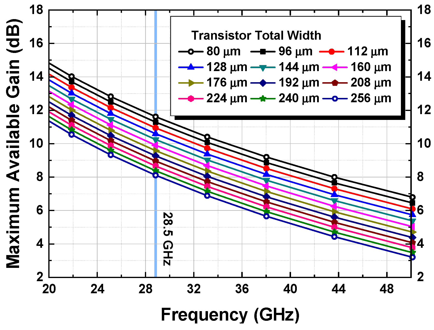
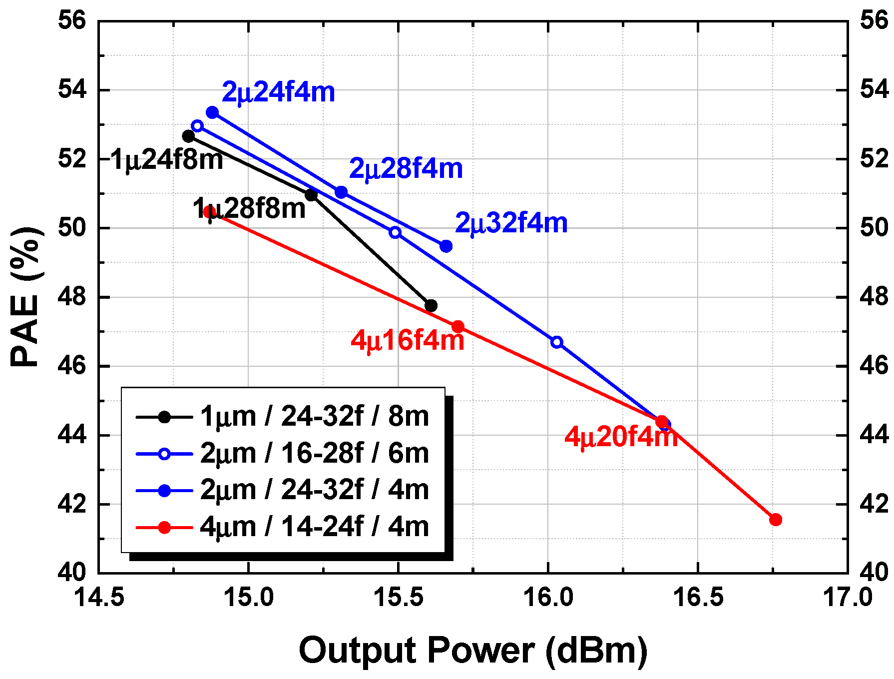
2.1. Size Determination of the Unit Amplifier Transistor

The RFCMOS transistors used in this study had a gate length of 65 nm with a maximum of 32 fingers. The gate lengths of the transistors used in this study are all 65 nm. The transistor size was adjusted by changing the width of the unit finger, total number of fingers, and multiplier. Figure 1 shows the maximum available gain (MAG) according to the transistor size at 350 mV gate bias voltage. As the gate width changes from 80 μm to 256 μm, the single-stage MAG ranges between 8 and 11.5 dB at 28.5 GHz.
To determine the size of the transistor unit cell and the power stage, simulation of the output power, PAE, and load-pull of the unit amplifier was conducted; moreover, electromagnetic (EM) simulations of the transistor connections in the multiplier were also conducted. As seen in Figure 2, the output power increases with an increase in transistor size. However, PAE decreases, indicating inefficiency in further increasing the transistor size to achieve increased output power. Therefore, it is important to determine the (i) size of the transistor unit cell of the power stage, (ii) target output power, and (iii) the PAE to determine the appropriate transistor size. Particularly, to determine the size of the transistor, we must first determine the finger width, number of fingers, and multiplier size; however, the performance differs in each case due to parasitics, as shown in Figure 2. For example, the smaller the finger width, the smaller is the parasitic gate resistance inside the transistor; therefore, the 4 μm finger width (red line) has a much lower PAE. For 1 μm finger width (black line), many multipliers must be used to achieve high power, which results in lower PAE owing to the parasitic component in the power cell layout. Thus, we used unit cell transistors in the power stage with a 2 μm finger width in this study. Additionally, 32 fingers and 4 multipliers (total gate width: 256 μm) were used to achieve the target output power of 15 dBm with margin. In this study, we designed a three-stage PA with transistor gate widths of 144, 192, and 256 μm for each stage with a MAG of 10.5, 9.5, and 8 dB, respectively, and an expected total gain of 28 dB.

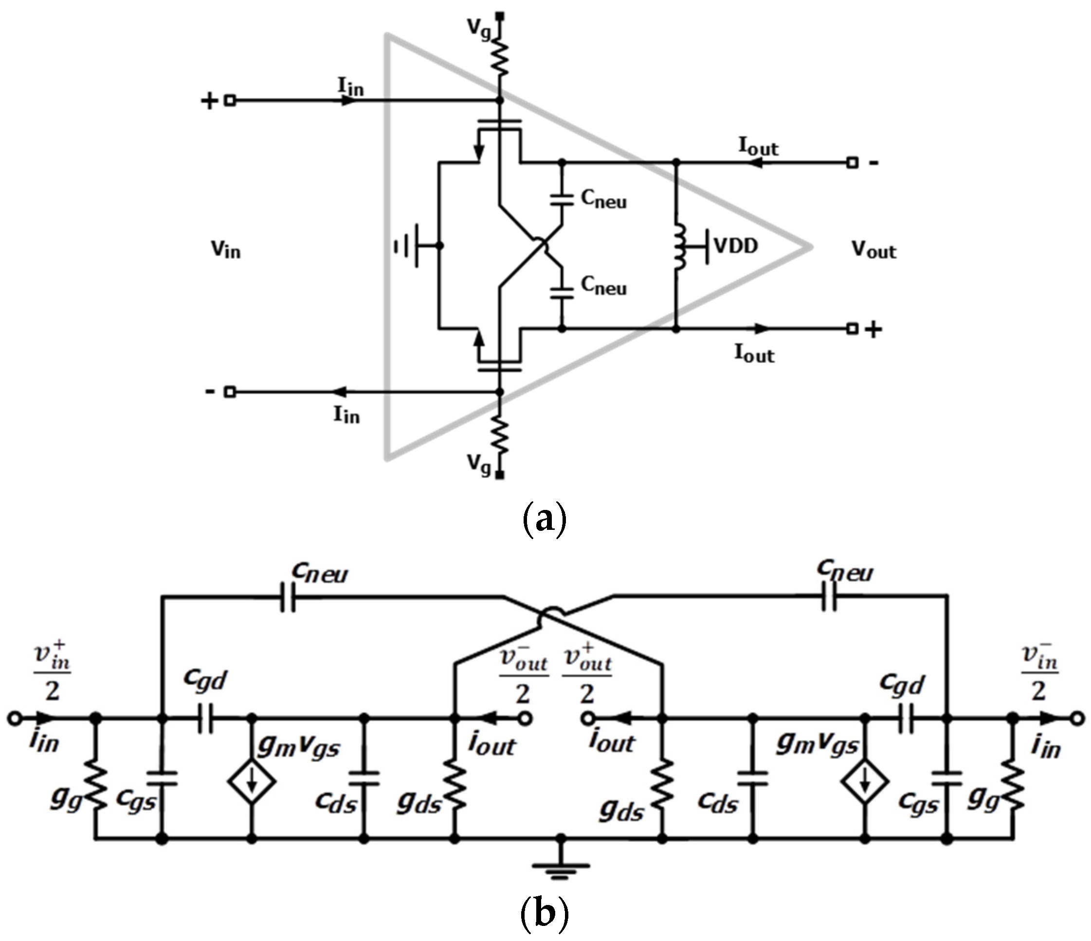
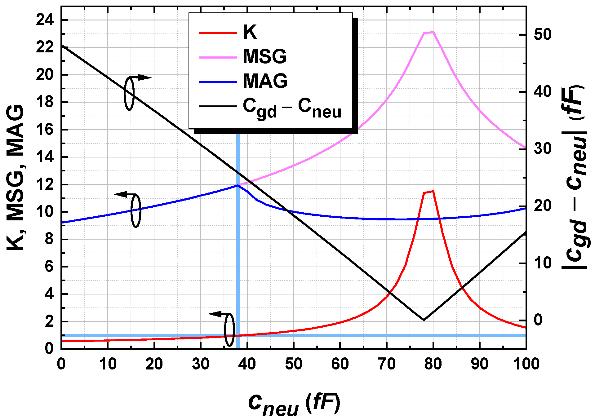
2.2. Size Determination and Analysis of the Neutralized Capacitor

Figure 3 shows the small-signal analysis model of the transistor. The admittance of each port is calculated using Equation (1). Each capacitance can be calculated individually, as shown in Equation (2).
y 11 = s C g s + s C g d   ,               y 12 = s C g d y 21 = g m s C g d   ,                     y 22 = g d s + s C d s + s C g d
C g d = i m   ( y 12 ) ω ,       C g s = i m   ( y 11 + y 12 ) ω ,       C g d = i m   ( y 22 + y 12 ) ω
For the transistor with 256 μm gate width (2 μm unit finger width × 32 fingers × 4 multipliers), the parasitic capacitances are estimated as Cgd = 72 fF, Cgs = 145 fF, and Cds = 149 fF. Among the three parasitic capacitances, Cgd in particular forms a feedback loop, resulting in instability in the PA. Therefore, to cancel out the Cgd, a capacitive neutralization method is generally used in the mm-wave PA. In general, the required neutralized capacitance Cneu is extracted by simulation tuning, however, in this study, quantitative Cneu was calculated based on Cgd value. We first utilized a differential structure including Cneu to offset the feedback loop, after which the value of Cneu was extracted and the small-signal analysis was conducted.
Figure 4a shows the circuit with Cneu applied to the differential common source structure. Figure 4b shows the schematic representation of the small-signal model of the circuit shown in Figure 4b. The admittance of each port in the small-signal analysis model is calculated as:
i i n = s C g s v i n         + + s C g d ( v i n           + 2 v o u t           2 ) + s C n e u ( v i n           + 2 v o u t           + 2 )             = s ( C g s + C g d + C n e u ) v i n           + 2 s ( C g d C n e u ) v o u t           2
i o u t = ( g d s + s C d s ) v o u t           + g m v i n           + 2                                                                                                 + s C g d ( v o u t           2 v i n           + 2 ) + s C n e u ( v o u t           2 v i n           2 )               = ( g m s C g d + s C n e u ) v i n           + 2 + ( g d s + s C g d + s C g d + s C n e u ) v o u t           2
Y = [ y 11 = i i n v i n | v o u t = 0 y 12 = i i n v o u t | v i n = 0 y 21 = i o u t v i n | v o u t = 0 y 22 = i o u t v o u t | v i n = 0 ] .
When Equations (3) and (4) are substituted in Equation (5) for the arrangement, the admittance of the alternative power cell is obtained and is given as:
y 11 = s C g s + s ( C g d + C n e u ) 2   ,           y 12 = s ( C g d C n e u ) 2 y 21 = g m s ( C g d C n e u ) 2   ,                 y 22 = g d s + s C d s + s ( C g d + C n e u ) 2
As seen in Equation (6), the capacitance of the differential structure is halved, as compared to the single-end structure. Further, the maximum stable gain (MSG), MAG, and stability factor (K) are calculated as [6]:
M S G = | y 21 | | y 12 | = | g m s ( C g d C n e u )   | | s ( C g d C n e u )   | = g m       2 + ω 2 ( C g d C n e u )   2 ω   | C g d C n e u |
M A G = M S G ( K K 2 1 )
K = 2 Re   {   y 11 } Re   {   y 22 } Re   {   y 12 y 21 } | y 12 y 21 |             = 2 g g g d s + ω 2 ( C g d C n e u )   2 ω   | C g d C n e u |   ω 2 ( C g d C n e u )   2 + g m     2
K     >     1   ,           Re   {   y 11 }     >     0   ,           Re   {   y 22 }     >     0
To conveniently determine K, a series parasitic resistance of the gate was equivalent to a parallel parasitic resistance, gg, to satisfy the condition in Equation (10). The simulation results of K, MSG, and MAG, based on the values of Cneu in a single-stage differential PA at 28 GHz, are shown in Figure 5. As | CgdCneu | decreases, K and MSG increase with smaller denominators and achieve the highest value when Cgd and Cneu are equal. Thus, adjusting the Cneu can deliver additional gain and stability in the PA. Consequently, although the oscillation risk is particularly high in the high-gain three-stage PA, this can be solved by analyzing the parasitic capacitance of the transistors and the subsequent optimization of capacitive neutralization.

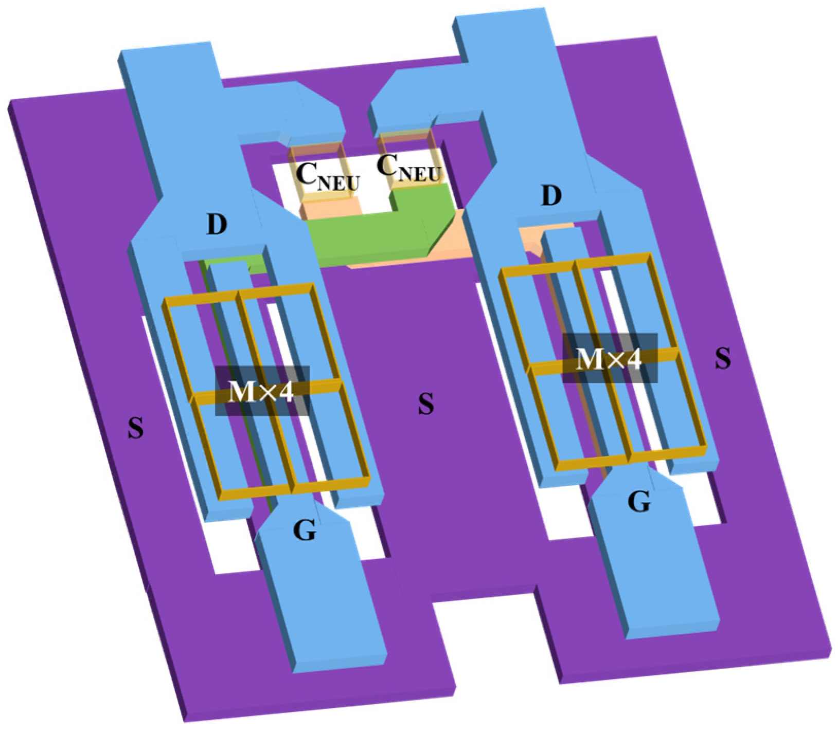
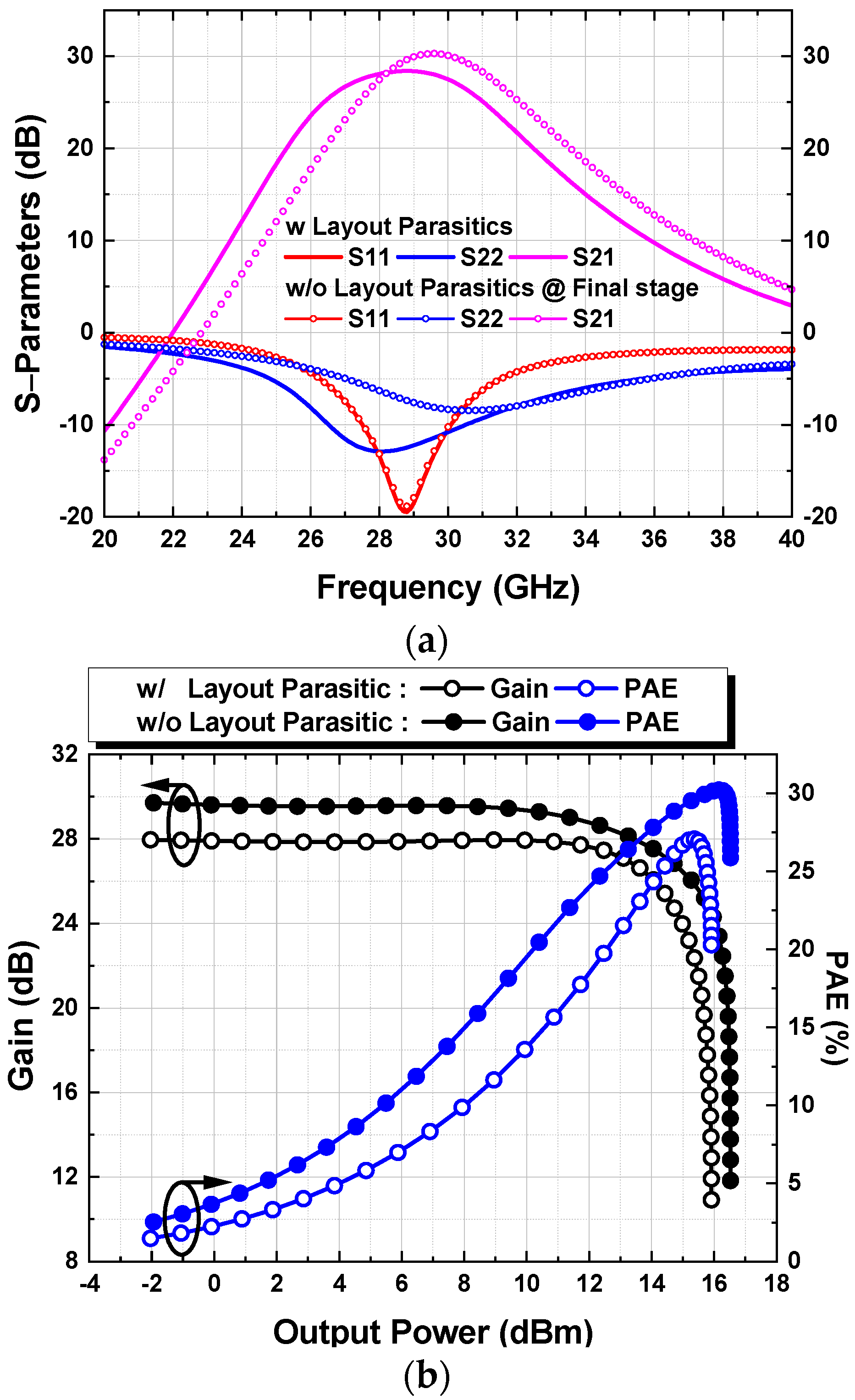
2.3. Analysis of Parasitices Caused by Power Cell Layout

Given that the power cell comprises several unit transistors, the parasitic components induced by various interconnecting lines and contacts are included in the simulation analysis to ensure accurate results. In this section, the effects of parasitic components are identified by comparing the schematic simulation results and the EM simulation results, while considering the layout of the power cell. Additionally, we present the analysis process in the power stage of the PA to ensure convenience.
Figure 6 shows the power cell layout of the designed PA, comprising of wide and long metal lines for interconnections, which generate various parasitic resistances, inductances, and capacitances. EM simulation was performed to consider the parasitic components of the power cell through the layout shown in Figure 6. Considering the interconnect lines and contacts, Cgd, Cgs, and Cds increase by 10%, to 7.7 fF, 19.9 fF, and 19.2 fF, respectively, which is sufficient to affect the overall performance of the PA.
The difference in the estimations with and without EM simulations based on the results from Figure 6 is shown in Figure 7. Figure 7a shows that the operating frequency was downshifted due to the additional parasitic capacitance extracted from the EM simulation of the power cell layout; moreover, considering the parasitic components induced by the first and second stages would cause severe performance degradation in the power cell. As shown in Figure 7b, from the results of the continuous wave simulation at each center frequency (with parasitic components: 28 GHz and w/o parasitic components: 30 GHz), we can confirm that loss is mainly caused by the parasitic resistance. Consequently, the gain and saturation output power decreased by 2 dB and 0.5 dB, respectively, and PAE decreased by 3%. Additionally, considering these parasitic components affect the optimization values of Cneu and have a significant impact on stability or bandwidth, an accurate EM analysis is required. In this study, the target operating frequency is 28.5 GHz, so the PA is designed by considering the downshift induced by the parasitic components of the power cell.

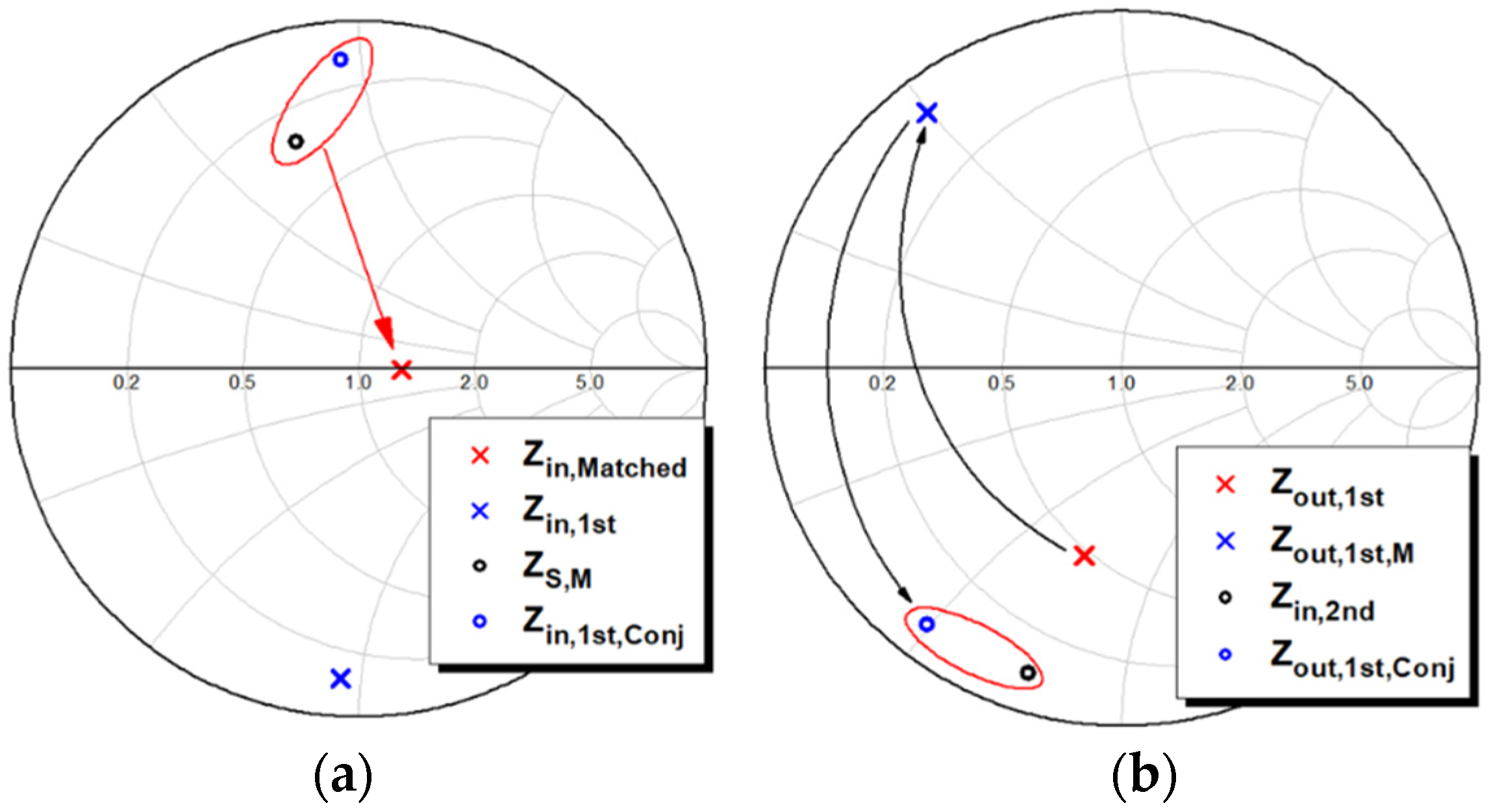
2.4. Configuration of Matching Network with Transformers
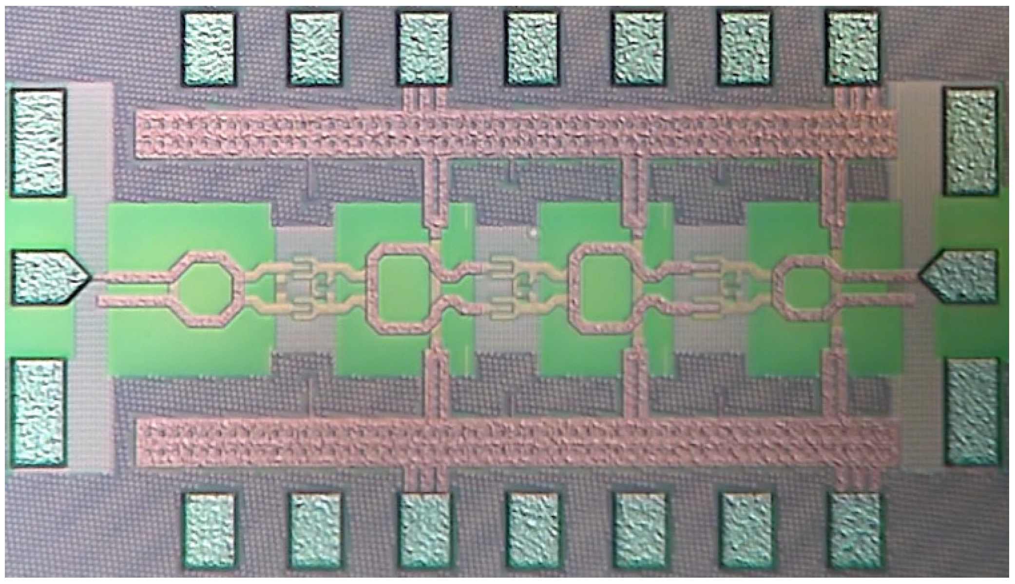
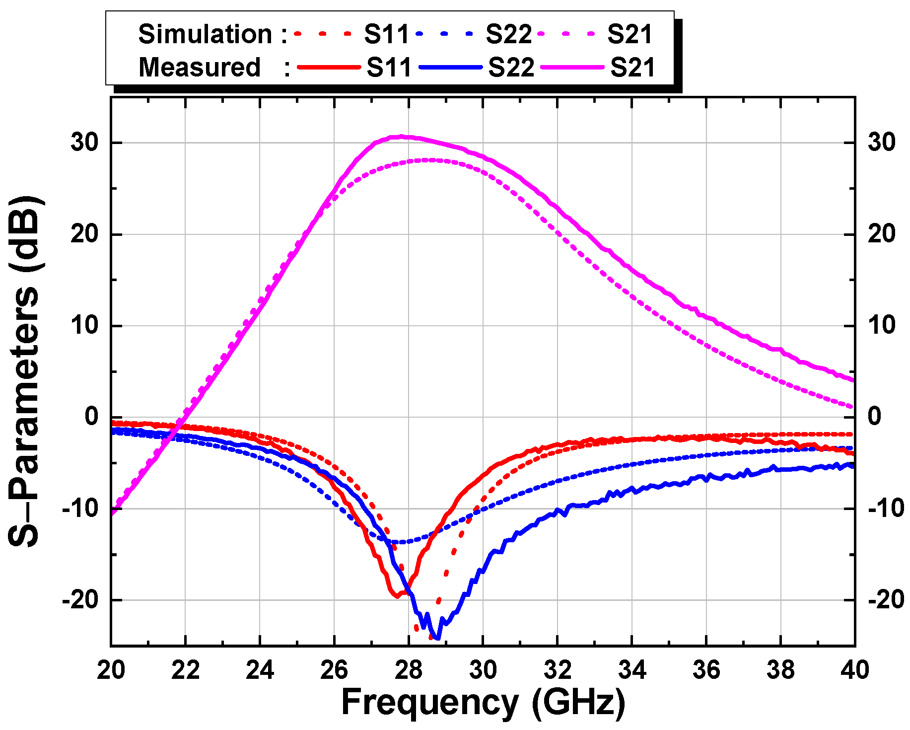
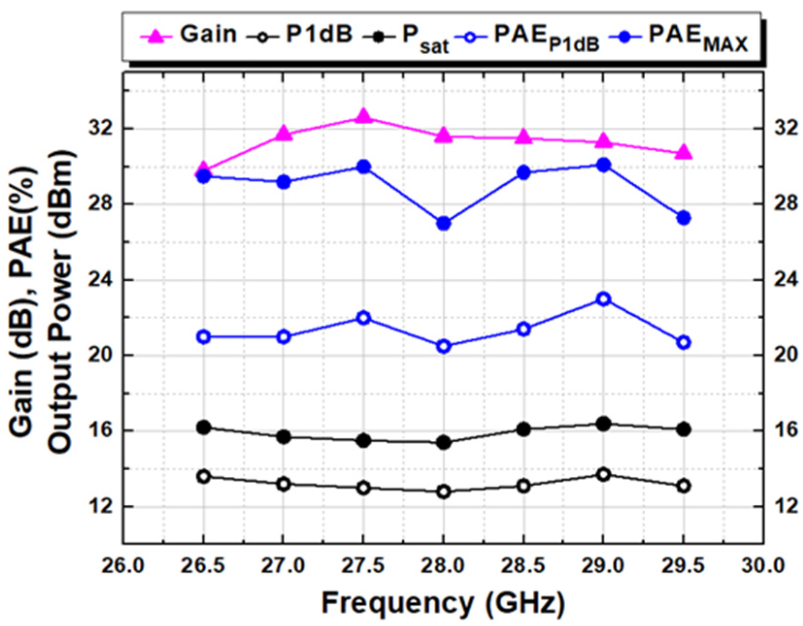
Figure 8 shows a schematic of the designed PA, which comprises a three-stage configuration, each stage consisting of a common source structure. The matching process at each stage is shown in Figure 9. The smith charts shown in Figure 9 were normalized to 50 Ω. Figure 9a shows the input and interstages matched with the conjugate to minimize loss during signal transmission. In the input matching network, ZS and input impedance of the first stage should match the conjugate. ZS,M should match ZS,1st,Conj as much as possible, through which, Zin,Matched is converted to 63.95 Ω close to 50 Ω. The input matching network was constructed considering the bandwidth rather than exact matching values. Figure 9b,c shows that the output impedances of the first and second stages are conjugate matched with the input impedance of the next stages through the inter-stage matching network. Finally, Figure 9d shows the process of matching ZL by obtaining the optimized output impedance ZOpt for maximum output power and PAE. Through load-pull simulation, ZOpt,Pout and ZOpt,PAE were found to be 13 + j8.9 Ω and 12.6 + j15.4 Ω, respectively. ZL is converted to 11 + j13.4 Ω through an output matching network (OMN) consisting of transformers and an output parallel capacitor (OPC). When the output impedance corresponds to ZOpt,Pout and ZOpt,PAE, the maximum output power and PAE are 15.4 dBm and 27.2%, respectively, and the expected values with 50 Ω load impedance are 15.3 dBm and 26.4%, respectively. The EM simulation was performed throughout the PA, including matching networks, transformers, pads, and connection lines between devices.

3. Measured Results

We designed a three-stage differential PA using a 65 nm RFCMOS, as seen in Figure 10 which shows a photograph of the designed PA. The total size of the PA, including the pads, was 0.90 × 0.50 mm2. and the core size of PA, excluding the pads and decoupling capacitors, was 0.74 × 0.16 mm2. The s-parameter and power of the designed PA was measured using Rohde-Schwarz ZNA43 vector network analyzer.
Figure 11 shows the S-parameter measurement results for the designed PA, which was measured in all three stages with a VDD of 1 V and gate bias voltages of 330/350/350 mV. The measured standby current of the PA was 47 mA, and the resulting current density of the transistor used was 40 μA/μm. From S21, the gain at 3 dB bandwidth is 4 GHz (26.5–30.4 GHz). The measured S11 and S22 were below −10 dB, ranging between 26.5–29.2 GHz and 26.8–32.2 GHz, respectively; the difference between the measurement and simulation results were due to variation in the process, and the two results were similar because of rigorous EM simulations. The measurement results of the CW signal under the specified bias conditions are shown in Figure 12. The PA has a saturated output power of 16.1 dBm at 28.5 GHz and 13.1 dBm at P1dB with a gain of 31.5 dB. The maximum PAE was 29.7%, whereas the PAE at P1dB was 22%. The measurement results of the CW signal are similar to that in the preceding chapter; however, it differs in current and gain due to variation in the process, resulting in a higher gain and PAE than that in the simulation. Figure 13 shows the measurement results of CW signals with frequencies ranging between 26.5–29.5 GHz. The maximum PAE of 30.1% was achieved at 29 GHz, over 27% in the higher bandwidths, and between 20.5–23% at P1dB. The output power P1dB ranged between 12.8–13.7 dBm, and the saturated output power ranges between 15.4–16.4 dBm.
Table 1 shows a comparison of the performance of a designed PA with that of other CMOS PAs. The designed PA had a relatively high gain of 31.5 db with a Psat of 16.1 dBm.

4. Conclusions

We designed a PA operating between the 26.5–29.5 GHz band using a 65 nm RFCMOS. The designed PA achieved a high gain of 30.7 dB at 27.8 GHz by optimizing the size of the power cell and neutral capacitor Cneu. Particularly, if a three-stage PA is configured, there is a rash risk due to high gain, and stability can be ensured only through strict EM simulations and analysis of parasitic components. The designed PA had a saturated power of 16.1 dBm—13.1 dBm at output P1dB, and a maximum PAE of 29.7%.

Author Contributions

Conceptualization, H.J., H.L. and C.P.; methodology, B.P. and S.J.; Investigation, B.P. and S.K.; supervision, writing—original draft, H.J. and C.P.; writing—review and editing, H.J., H.L., B.P., S.J., S.K. and C.P. All authors have read and agreed to the published version of the manuscript.

Funding

This research was funded by Institute of Information & Communications Technology Planning & Evaluation (IITP) grant funded by the Korea government (MSIT) (2019-0-00933, Development on multi-beam antenna technology).

Institutional Review Board Statement

Not applicable.

Informed Consent Statement

Not applicable.

Data Availability Statement

The data can be received from the authors on request.

Conflicts of Interest

The authors declare no conflict of interest.

References

  1. Zong, Z.; Tang, X.; Khalaf, K.; Yan, D.; Mangraviti, G.; Nguyen, J.; Liu, Y.; Wambacq, P. A 28-GHz SOI-CMOS Doherty power amplifier with a compact transformer-based output combiner. IEEE Trans. Microw. Theory Tech. 2021, 69, 2795–2808. [Google Scholar] [CrossRef]
  2. Park, J.; Kang, S.; Hong, S. Design of a Ka-band cascode power amplifier linearized with cold-FET interstage matching network. IEEE Trans. Microw. Theory Tech. 2021, 69, 1429–1438. [Google Scholar] [CrossRef]
  3. Cho, G.; Jeong, G.; Hong, S. 28-GHz CMOS power amplifier linearized with resistive drain-body connection. IEEE Microw. Wirel. Compon. Lett. 2020, 30, 876–879. [Google Scholar] [CrossRef]
  4. Ding, B.; Yuan, S.; Zhao, C.; Tao, L.; Tian, T. A Ka band FMCW transceiver front-end with 2-GHz bandwidth in 65-nm CMOS. IEEE Trans. Circuits Syst. II Express Briefs 2019, 66, 212–216. [Google Scholar] [CrossRef]
  5. Jia, H.; Prawoto, C.C.; Chi, B.; Wang, Z.; Yue, C.P. A full Ka-band power amplifier with 32.9% PAE and 15.3-dBm power in 65-nm CMOS. IEEE Trans. Circuits Syst. I Regul. Pap. 2018, 65, 2657–2668. [Google Scholar] [CrossRef]
  6. Deferm, N.; Reynaert, P. CMOS at millimeter wave frequencies. In CMOS Front Ends for Millimeter Wave Wireless Communication Systems; Springer: Berlin/Heidelberg, Germany, 2015; pp. 13–25. [Google Scholar]
  7. Chen, Y.-C.; Lin, Y.-H.; Lin, J.-L.; Wang, H. A Ka-band transformer-based Doherty power amplifier for multi-Gb/s application in 90-nm CMOS. IEEE Microw. Wirel. Compon. Lett. 2018, 28, 1134–1136. [Google Scholar] [CrossRef]
  8. Indirayanti, P.; Reynaert, P. A 32-GHz 20-dBm PSAT transformer-based Doherty power amplifier for multi-Gb/s 5G applications in 28-nm bulk CMOS. In Proceedings of the 2017 IEEE Radio Frequency Integrated Circuits Symposium, Honolulu, HI, USA, 4–6 June 2017; pp. 45–48. [Google Scholar]
  9. Lee, J.; Hong, S. A 24–30 GHz 31.7% fractional bandwidth power amplifier with an adaptive capacitance linearizer. IEEE Trans. Circuits Syst. II Express Briefs 2021, 68, 1163–1167. [Google Scholar] [CrossRef]
  10. Manente, D.; Padovan, F.; Seebacher, D.; Bassi, M.; Bevilacqua, A. A 28-GHz stacked power amplifier with 20.7-dBm output P1dB in 28-nm bulk CMOS. IEEE Solid-State Circuits Lett. 2020, 3, 170–173. [Google Scholar] [CrossRef]
Figure 1. MAG of the unit amplifier based on the transistor gate width.
Applsci 11 11691 g001
Figure 2. Load-pull simulation result of the unit amplifier based on the transistor size.
Applsci 11 11691 g002
Figure 3. Small signal analysis model of the common source transistor.
Applsci 11 11691 g003
Figure 4. Schematic representation of (a) differential common source power cell, (b) small signal analysis model of (a).
Applsci 11 11691 g004
Figure 5. Simulated result of stability factor, MSG, and MAG.
Applsci 11 11691 g005
Figure 6. Power cell layout for the proposed design.
Applsci 11 11691 g006
Figure 7. Simulation result of (a) s-parameters and (b) gain. PAE with or without power cell layout parasitic components in the power stage of three-stage PA.
Applsci 11 11691 g007
Figure 8. Schematic of the proposed three-stage PA.
Applsci 11 11691 g008
Figure 9. Simulation results of matching networks: (a) input conjugate matching, (b) conjugate matching for first and second stages, (c) conjugate matching for second and power stages, and (d) output matching for ZL with Zopt through load-pull simulation.
Applsci 11 11691 g009aApplsci 11 11691 g009b
Figure 10. Chip photograph of designed three-stage PA.
Applsci 11 11691 g010
Figure 11. Measured s-parameters (solid) and simulated s-parameters (dot).
Applsci 11 11691 g011
Figure 12. Measured gain and PAE versus output power with CW signal.
Applsci 11 11691 g012
Figure 13. Results of CW signal measurements by frequency.
Applsci 11 11691 g013
Table 1. Performance comparison with state-of the art CMOS PAs.
Ref.Tech.Freq.
(GHz)
Supply
(V)
Psat
(dBm)
P1dB
(dBm)
Gain
(dB)
Peak PAE
(%)
Architecture
This work65 nm28.51.016.113.131.529.7Three-stage
CS
TMTT’ 21
[2]
65 nm312.217.11518.938.2Two-stage
Cascode
TCASII’ ‘21
[9]
28 nm262.220.318.221.233.1Two-stage
Cascode
SSCL’20
[10]
28 nm281.821.520.720.426Two-Stacked
Four way
Publisher’s Note: MDPI stays neutral with regard to jurisdictional claims in published maps and institutional affiliations.

