Article

Enhancing SERS Intensity by Coupling PSPR and LSPR in a Crater Structure with Ag Nanowires

1
Department of Electronic Materials Engineering, Korea Maritime & Ocean University, Busan 49112, Korea
2
Interdisciplinary Major of Maritime AI Convergence, Korea Maritime & Ocean University, Busan 49112, Korea
3
Division of Advanced Technology, Korea Research Institute of Standards and Science, Daejeon 34113, Korea
*
Author to whom correspondence should be addressed.
These authors contributed equally to this work.
Appl. Sci. 2021, 11(24), 11855; https://doi.org/10.3390/app112411855
Submission received: 13 November 2021 / Revised: 27 November 2021 / Accepted: 10 December 2021 / Published: 13 December 2021

Abstract

:
The sensitive characteristics of surface-enhanced Raman scattering (SERS) can be applied to various fields, and this has been of interest to many researchers. Propagating surface plasmon resonance (PSPR) was initially utilized but, recently, it has been studied coupled with localized surface plasmon resonance that occurs in metal nanostructures. In this study, a new type of metal microstructure, named crater, was used for generating PSPR and Ag nanowires (AgNWs) for the generation of LSPR. A crater structure was fabricated on a GaAs (100) wafer using the wet chemical etching method. Then, a metal film was deposited inside the crater, and AgNWs were uniformly coated inside using the spray coating method. Metal films were used to enhance the electromagnetic field when coupled with AgNWs to obtain a high SERS intensity. The SERS intensity measured inside the crater structure with deposited AgNWs was up to 17.4 times higher than that of the flat structure with a deposited Ag film. These results suggest a new method for enhancing the SERS phenomenon, and it is expected that a larger SERS intensity can be obtained by fine-tuning the crater size and diameter and the length of the AgNWs.

1. Introduction

Surface plasmon resonance (SPR) is a phenomenon in which free electrons within the metal surface oscillate collectively when light is irradiated on the metal-dielectric interface [1,2]. SPR is classified into two types: propagating surface plasmon resonance (PSPR), which occurs in the form of surface plasmon polaritons (SPPs) along smooth metal–dielectric interfaces, and localized surface plasmon resonance (LSPR), which is generated locally between metal nanostructures [3]. There are several methods for generating SPR, such as making micro- and nano-sized holes [4,5] or creating a rough surface using nanoparticles [6,7], nanospheres [8,9], and nanowires [10,11] on metal films such as Ag and Au. The electric field is enhanced through resonance between the incident light source that has a specific wavelength, and either a sharp corner of the metal nanostructures or the narrow gap between the nanoparticles, which is called the “hot spot” [12]. The electromagnetic field can, therefore, be enhanced by generating PSPR and LSPR through these various methods, but the enhancement effect is limited when only one type of SPR exists. A higher electromagnetic field enhancement can be obtained by coupling PSPR with metal micro and nanostructures and LSPR by hot spots on the surface [13]. For example, Abutoama et al. obtained ultra-high field enhancement through coupling localized and propagating surface plasmons by fabricating grating geometry structures and depositing nanoparticles [14]. The enhanced electromagnetic field causes a surface-enhanced Raman scattering (SERS) phenomenon in which a weak Raman signal due to a small scattering cross-sectional area is greatly amplified [15]. SERS is a key interest of many researchers because it can be applied to various fields, such as marine environment, medicine, food science, biology, and optics, as a sensitive technology for detecting very low concentrations of molecules [16,17,18,19]. In particular, SERS is very useful for searching various poisons or toxins present in seawater or ocean creatures. Cao et al. analyzed saxitoxin using cysteine-modified Au nanoparticles [20]. And Schmidt et al. detected poly-nuclear aromatic hydrocarbons with high carcinogenicity using Ag colloid as a SERS probe [21]. One method of creating SERS is to use Ag nanowires (AgNWs), which are one-dimensional metal nanostructures with a high aspect ratio. They are widely used as transparent electrodes due to their excellent electrical conductivity and optical transparency [22]. Additionally, they are suitable nanostructures for producing the SERS phenomenon due to their large surface area, good crystallinity, and wide plasma resonance band between the UV to the near-infrared region [23,24]. Kang et al. enhanced SERS intensity by crossing a pair of metal nanowires [25]. Chen et al. fabricated a layer-by-layer assembly of AgNWs to obtain high-density hot spots [26]. Yoon et al. fabricated a simple SERS architecture by forming hot spots between a metal film and a nanowire [27]. In this case, the substrate for SERS requires a uniform distribution of nanostructures for the uniformity and stability of the Raman signal. To create a uniform distribution, the self-assembled monolayer, electrochemical deposition, and spray coating methods are adopted [28,29,30]. Within this study, the spray coating method was chosen and applied, which deposits relatively uniformly over a large area. To further enhance the SERS effect, a volcanic crater type structure capable of condensing light was fabricated, and a metal film and the AgNWs were sequentially deposited therein. The deposited AgNWs form a high-density hot spot due to the gap between the AgNWs and the metal film. Thus, the LSPR generated by a hot spot can be coupled to the PSPR generated by the metal film deposited inside the crater. The enhancement of the electric field was analyzed through SERS measurements taken from inside the crater and the flat surface, and these are explained in relation to the FDTD simulation result.

2. Experimental Procedure

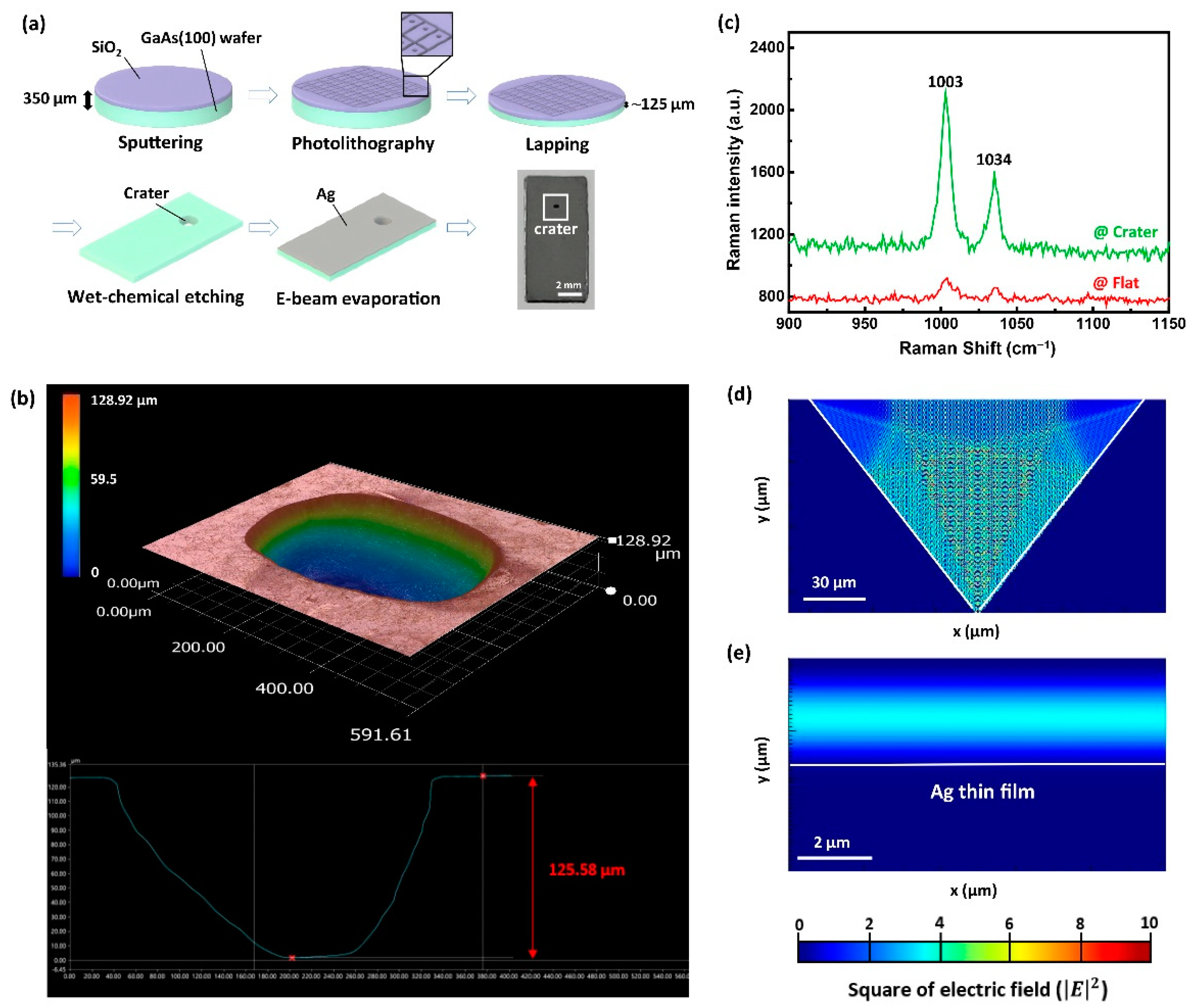
2.1. Fabrication of Crater Structures

A 300 nm thick SiO2 thin film was deposited on a 350 µm thick GaAs (100) by RF sputtering. To make circular patterns with a diameter of 50 µm on the SiO2 thin film, we first performed ultrasonication using acetone, methanol, and deionized water for 5 min, sequentially. Moisture was removed with N2 gas, and then a wafer was placed on a hot plate at 90 °C for 10 min to completely remove the remaining moisture. In the second process, the photoresist (GXR-601) was spin-coated on a wafer, and then soft baking was performed on a hot plate at 90 °C for photolithography. Finally, the pattern was formed by exposing the wafer to UV light for 10 s and developing it for 30 s. To control the size of the crater, lapping was performed on the bottom of the substrate to a thickness of 100–125 µm for 2 h. A wafer was attached to the slide glass with transparent rosin, and a crater structure was fabricated using the wet chemical etching method, with an etching solution prepared with a volume ratio of H2SO4:H2O2:H2O = 1:5:5.

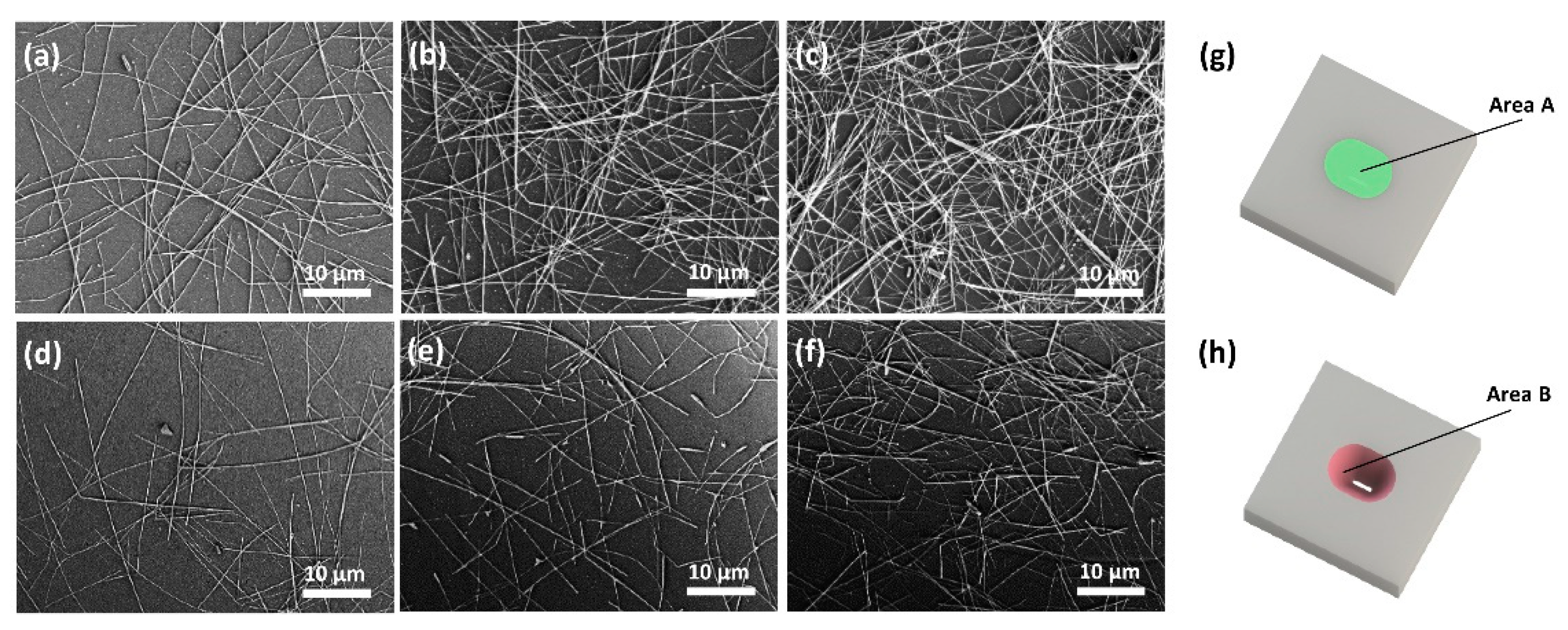
2.2. Spray Coating of Ag Nanowires (AgNWs)

To control the density of the AgNWs, the AgNWs suspension was diluted with ethanol to prepare a concentration of 2 mg/cm3. The AgNWs in the suspension were evenly dispersed through ultrasonication. The AgNWs suspension was sprayed vertically 22 cm from the sample that was placed on a hot plate at 150 °C. Finally, the sample was heated on a hot plate at 150 °C for 1 min to evaporate the remaining ethanol.

2.3. Characterization

The fabricated crater structure was analyzed using a high-resolution 3D microscope (VHX-7000, KEYENCE, Osaka, Japan). AgNWs were characterized using field-emission scanning electron microscopy (FE-SEM, CLARA, Tescan, Brno, Czech Republic).
Raman spectra was obtained using UniDRON (UNinanotechnology, Yongin, Korea). Each sample was measured using a 10× objective lens and a laser with a wavelength of 532 nm while immersed in 0.1 M aqueous solution of pyridine. The power of the incident laser was approximately ~0.5 mW and the exposure time was set to 20 s for all measurements. The error bars were calculated from the data obtained by measuring several parts of the same sample.

2.4. Finite-Difference Time Domain (FDTD) Simulations

In this study, the FDTD simulation conditions were as follows: (1) The top and bottom layers of the FDTD region absorbed light fully without reflection, indicating that they were perfectly matched, and an asymmetric boundary condition was applied because the structure is symmetrical about the y-axis. (2) A simulation time of 10,000 fs was sufficient to simulate the exact plasmon phenomenon. (3) The electric-field monitor was set up to contain part of the object, and mesh sizes of 0.1 nm × 0.1 nm × 0.1 nm were applied. (4) A total-field scattered-field source with a wavelength of 532 nm was propagated along the y-axis at the top of the object. (5) The nanowires and thin film that met the light in the simulation were silver, gold, and GaAs.

3. Results and Discussion

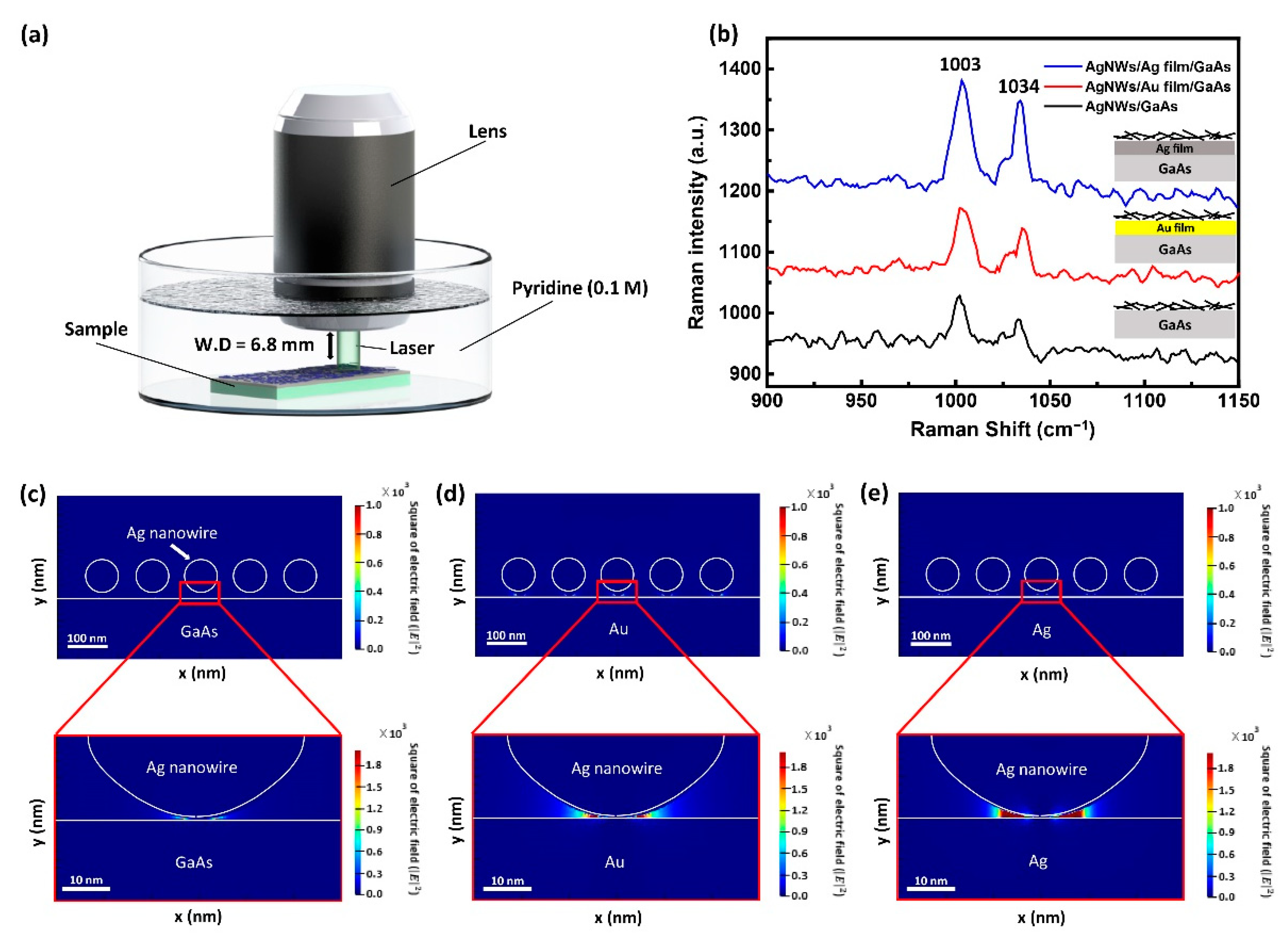
3.1. Finding a Metal with Excellent Surface-Enhanced Raman Scattering (SERS) Properties When Combined with AgNWs

First, to determine which metal film has high SERS properties when combined with AgNWs, we prepared 2 nm thick Au and Ag films on GaAs (100) substrates, and 4 cm3 of AgNWs/ethanol dispersion was spray-coated on each sample. The average diameter and length of the AgNWs were approximately 70 nm and 50 µm, respectively. Raman measurements were performed to compare the SERS characteristics according to the metal films, and the schematic is shown in Figure 1a.
Figure 1b shows a comparison of the SERS intensities of AgNWs deposited on Ag/GaAs, Au/GaAs, and GaAs substrates. For the samples, the Raman peaks of pyridine were observed at the same positions of 1003 cm−1 and 1034 cm−1. Comparing the SERS intensities at 1003 cm−1 showed that the intensity of the substrate with the Ag film was the largest, and the SERS intensity of AgNWs/Agfilm/GaAs was approximately 2.23 times that of the AgNWs/GaAs. This indicates that the electric field is enhanced by the LSPR generated in the gap between the AgNWs and Ag film. In addition, the SERS intensity of AgNWs/Agfilm/GaAs was approximately 1.6 times stronger than that of AgNWs/Aufilm/GaAs. This may be explained by the longer SPPs propagation length of Ag compared to that of Au and, thus, a greater electric field enhancement was observed in the gap between the Ag film and AgNWs and among the AgNWs [31]. To investigate the electric field distribution resulting from the metal film, FDTD simulations were performed for each condition, and the results are shown in Figure 1c–e. The diameter and length of the AgNWs were set to approximately 70 nm and 50 µm, respectively, and the gap between the AgNWs was set to 50 nm. As shown in Figure 1c, there was a weak electric field enhancement between the AgNWs-GaAs substrate. Conversely, a strong local field was confirmed between the AgNWs and metal film, as shown in Figure 1d,e. In particular, the largest electric field enhancement was observed in the AgNWs-Ag, implying that the surface plasmon coupling between the AgNWs and Ag films is superior to that of the other films.

3.2. Fabrication of Ag Crater Structures and Characterization of SERS

The crater structure for condensing light was fabricated by wet chemical etching on a GaAs (100) wafer [32], a schematic of which is shown in Figure 2a.
We deposited 2 nm-thick Ag film inside the crater using the e-beam evaporation method. The crater was analyzed using a high-resolution optical 3D surface analyzer, and the measured 3D image is shown in Figure 2b. As can be seen from the depth profile, the crater was etched to a depth of 125 µm. To confirm that the electric field intensity inside the crater becomes stronger, the Raman spectrum was measured inside the crater and outside the crater (flat), and the results are shown in Figure 2c. All measurements were carried out under the same conditions as those shown in Figure 1b. The Raman peaks of pyridine in the crater and flat structures were observed at the same position of 1003 cm−1 and 1034 cm−1. At the pyridine Raman peak position (1003 cm−1), the SERS intensity inside the crater was approximately 7.78 times higher than that of the flat structure. It was concluded that the SERS intensity was enhanced because of the strong PSPR caused by the micro-sized crater structure and Ag film. For comparison with the experimental data, the electric field distribution inside the crater and on the flat 2 nm-thick deposited Ag was analyzed through the FDTD simulation, and the results are shown in Figure 2d,e. The crater structure was fabricated using the 3D AutoCAD program. Comparing Figure 2d,e shows that the electric field inside the crater tends to be stronger than that of the flat surface. This enhancement can be attributed to the effect of the crater structure.

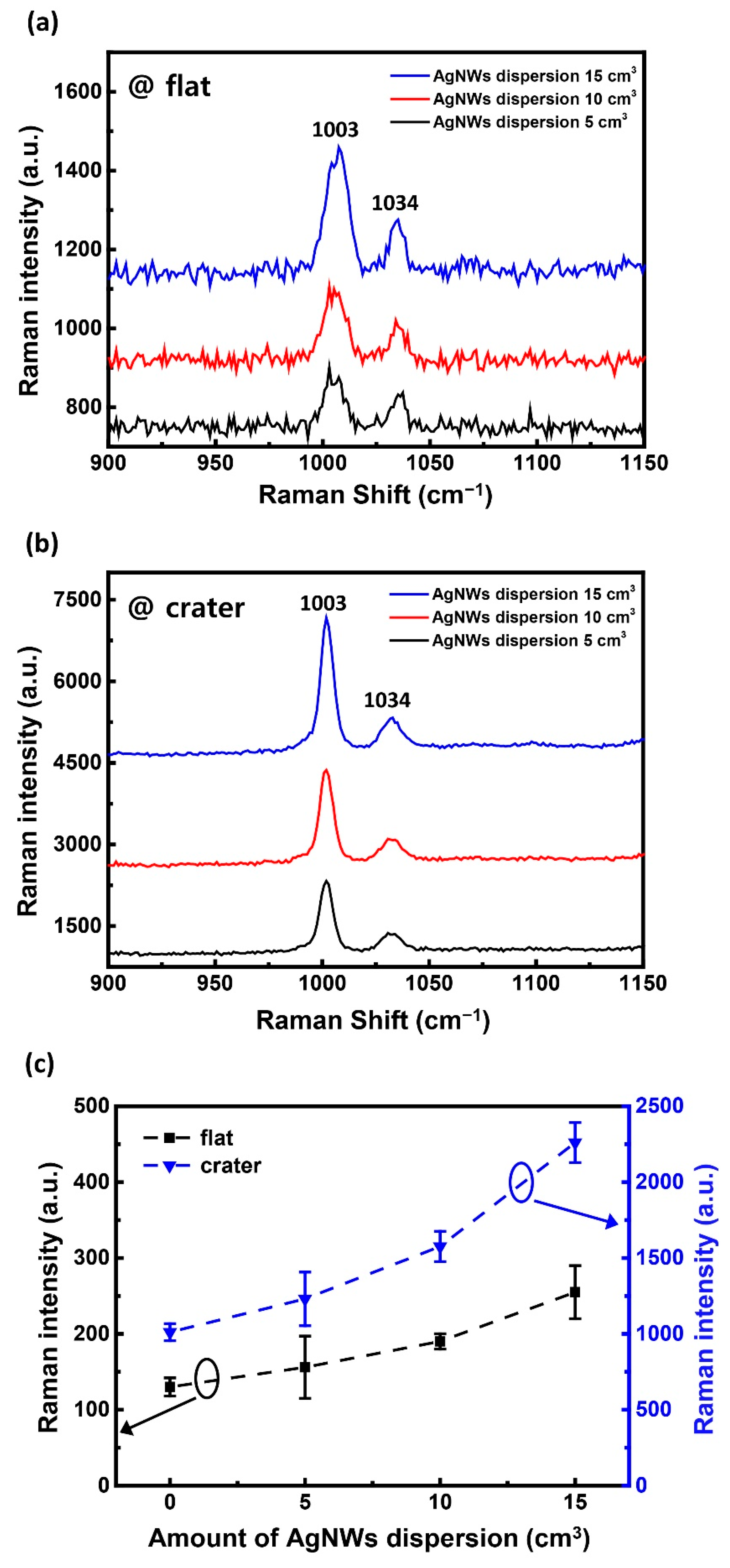
3.3. Coupling of the Ag Crater Structure and AgNWs

To generate strong field enhancement by coupling with the LSPR and PSPR, 5, 10, and 15 cm3 of AgNWs dispersion was spray-coated on the inside of the crater and the flat, respectively. The morphology of AgNWs was measured using FE-SEM, as shown in Figure 3a–f.
The AgNWs were coated almost uniformly on the entire surface of both the flat and the crater. Additionally, as the amount of the AgNWs dispersion was increased, the density of AgNWs and the number of AgNW junctions also increased. However, under the same conditions, the density of AgNWs inside the crater was lower than that of the flat, which is explained by the difference in area as shown in Figure 3g,h. Here, areas A and B represent the flat area of the top surface of the crater and the inclined area inside the crater, respectively. Area B is approximately 1.72 times larger than Area A. Therefore, if the same amount of AgNWs dispersion is coated, the density of AgNWs inside the crater is lower.
Figure 4a shows the Raman spectrum of 0.1 M pyridine molecules on the flat surface when coated with 5, 10, and 15 cm3 of AgNWs dispersion.
Similar to the previous result, the Raman intensity appeared at the peak positions of 1003 cm−1 and 1034 cm−1 for the aqueous pyridine solution. The Raman intensity was amplified as the amount of the coated AgNWs dispersion was increased due to the strong plasmon coupling between the Ag film and the AgNWs, and among the AgNWs. Figure 4b shows the Raman spectrum of the pyridine molecules adsorbed inside the crater under the same conditions as those in Figure 4a. The SERS intensity inside the crater structure was amplified as the amount of AgNWs dispersion increased. Therefore, the high density of AgNWs on both the flat surface and in the crater forms numerous hot spots, contributing to the strong SERS enhancement. Figure 4c shows the Raman intensity on the flat and inside the crater structures at the pyridine peak position of 1003 cm−1, according to the amount of AgNWs. For the crater coated with 15 cm3 of AgNWs dispersion, the SERS intensity was enhanced by approximately 17.4 times more than it was on the flat surface without the presence of the AgNWs. Despite the low density of AgNWs inside the crater, the higher Raman signal than that of the flat surface can be explained by the SERS effect in the crater structure, as demonstrated above. This is due to the strong coupling between the LSPR generated by the densely coated AgNWs and the PSPR generated by the crater, which is a metal microstructure. In addition, if the density of AgNWs in the crater increases, a larger SERS effect can be expected.

4. Conclusions

We fabricated a micro-sized crater structure on a GaAs (100) wafer through wet chemical etching. After uniformly coating the AgNWs, we investigated the amplification of Raman intensity. Materials were determined as Ag and AgNWs by analyzing the conditions under which plasmon coupling occurs strongly, through Raman measurements and FDTD simulations. Raman signals from the flat surface and the crater were measured to confirm that the electric field had been enhanced inside the crater. In addition, Raman intensity showed the same tendency as the FDTD simulation data. The SERS intensity with 15 cm3 of AgNWs dispersion in the crater was 17.4 times higher than that on the flat surface without the presence of the AgNWs. We concluded that the amplified SERS intensity results from the strong coupling of the PSPR by the Ag crater structure and that of the LSPR by the Ag film and the AgNWs, and among the AgNWs. Using these results, we will apply it to the fabrication of the marine poison detection sensor.

Author Contributions

J.-H.R., H.-S.K. and S.-H.K. carried out the fabrication of the samples. H.Y.L. performed the high-resolution 3D microscope measurement and FDTD simulation. J.-H.R. performed the Raman spectroscopy measurement. J.-H.R., J.-Y.L. and H.Y.L. performed FE-SEM measurements. H.S.A., D.H.H. and S.N.Y. contributed to the interpretation of the data. J.-H.R., H.Y.L. and S.N.Y. contributed to the writing of the manuscript. S.N.Y. supervised the project. All authors have read and agreed to the published version of the manuscript.

Funding

This research was funded by the National Research Foundation of Korea (NRF), grant number 2020R1H1A2102133 and Korea Institute for Advancement of Technology (KIAT), grant number P0012451.

Institutional Review Board Statement

Not applicable.

Informed Consent Statement

Not applicable.

Data Availability Statement

The data that support the findings of this study are available from the corresponding author upon reasonable request.

Conflicts of Interest

The authors declare no conflict of interest.

References

  1. Ritchie, R.H. Plasma Losses by Fast Electrons in Thin Films. Phys. Rev. 1957, 106, 874–881. [Google Scholar] [CrossRef]
  2. Homola, J.; Yee, S.S.; Gauglitz, G. Surface Plasmon Resonance Sensors: Review. Sens. Actuators B Chem. 1999, 54, 3–15. [Google Scholar] [CrossRef]
  3. Zhang, Z.L.; Fang, Y.R.; Wang, W.H.; Chen, L.; Sun, M.T. Propagating Surface Plasmon Polaritons: Towards Applications for Remote-Excitation Surface Catalytic Reactions. Adv. Sci. 2016, 3, 1500215. [Google Scholar] [CrossRef] [PubMed]
  4. Wang, L.; Xu, B.; Bai, W.; Zhang, J.; Cai, L.; Hu, H.; Song, G. Multiple Surface Plasmon Resonances in Compound Structure with Metallic Nanoparticle and Nanohole Arrays. Plasmonics 2012, 7, 659–663. [Google Scholar] [CrossRef]
  5. Yi, Z.; Liu, M.; Luo, J.; Zhao, Y.; Zhang, W.; Yi, Y.; Yi, Y.; Duan, T.; Wang, C.; Tang, Y. Multiple Surface Plasmon Resonances of Square Lattice Nanohole Arrays in Au-SiO2-Au Multilayer Films. Opt. Commun. 2017, 390, 1–6. [Google Scholar] [CrossRef]
  6. Wei, H.; Xu, H. Hot Spots in Different Metal Nanostructures for Plasmon-Enhanced Raman Spectroscopy. Nanoscale 2013, 5, 10794–10805. [Google Scholar] [CrossRef] [PubMed]
  7. Wang, Z.B.; Luk’yanchuk, B.S.; Guo, W.; Edwardson, S.P.; Whitehead, D.J.; Li, L.; Liu, Z.; Watkins, K.G. The Influences of Particle Number on Hot Spots in Strongly Coupled Metal Nanoparticles Chain. J. Chem. Phys. 2008, 128, 94705. [Google Scholar] [CrossRef]
  8. Dick, L.A.; McFarland, A.D.; Haynes, C.L.; van Duyne, R.P. Metal Film over Nanosphere (MFON) Electrodes for Surface-Enhanced Raman Spectroscopy (SERS): Improvements in Surface Nanostructure Stability and Suppression of Irreversible Loss. J. Phys. Chem. B 2002, 106, 853–860. [Google Scholar] [CrossRef]
  9. Liu, K.; Bai, Y.; Zhang, L.; Yang, Z.; Fan, Q.; Zheng, H.; Yin, Y.; Gao, C. Porous Au-Ag Nanospheres with High-Density and Highly Accessible Hotspots for SERS Analysis. Nano Lett. 2016, 16, 3675–3681. [Google Scholar] [CrossRef] [PubMed]
  10. Jang, S.; Lee, J.; Nam, S.; Ko, H.; Chang, S.T. Large-Area, Highly Sensitive SERS Substrates with Silver Nanowire Thin Films Coated by Microliter-Scale Solution Process. Nanoscale Res. Lett. 2017, 12, 581. [Google Scholar] [CrossRef] [Green Version]
  11. Pandey, P.; Vongphachanh, S.; Yoon, J.; Kim, B.; Choi, C.J.; Sohn, J.I.; Hong, W.K. Silver Nanowire-Network-Film-Coated Soft Substrates with Wrinkled Surfaces for Use as Stretchable Surface Enhanced Raman Scattering Sensors. J. Alloy. Compd. 2021, 859, 157862. [Google Scholar] [CrossRef]
  12. Lee, J.; Hua, B.; Park, S.; Ha, M.; Lee, Y.; Fan, Z.; Ko, H. Tailoring Surface Plasmons of High-Density Gold Nanostar Assemblies on Metal Films for Surface-Enhanced Raman Spectroscopy. Nanoscale 2014, 6, 616–623. [Google Scholar] [CrossRef] [PubMed] [Green Version]
  13. Wang, X.; Wu, Y.; Wen, X.; Zhu, J.; Bai, X.; Qi, Y.; Yang, H. Surface Plasmons and SERS Application of Au Nanodisk Array and Au Thin Film Composite Structure. Opt. Quantum Electron. 2020, 52, 238. [Google Scholar] [CrossRef]
  14. Abutoama, M.; Li, S.; Abdulhalim, I. Widening the Spectral Range of Ultrahigh Field Enhancement by Efficient Coupling of Localized to Extended Plasmons and Cavity Resonances in Grating Geometry. J. Phys. Chem. C 2017, 121, 27612–27623. [Google Scholar] [CrossRef]
  15. Nie, S.; Emory, S.R. Probing Single Molecules and Single Nanoparticles by Surface-Enhanced Raman Scattering. Science 1997, 275, 1102–1106. [Google Scholar] [CrossRef] [PubMed]
  16. Lane, L.A.; Qian, X.; Nie, S. SERS Nanoparticles in Medicine: From Label-Free Detection to Spectroscopic Tagging. Chem. Rev. 2015, 115, 10489–10529. [Google Scholar] [CrossRef]
  17. Lin, Z.; He, L. Recent Advance in SERS Techniques for Food Safety and Quality Analysis: A Brief Review. Curr. Opin. Food Sci. 2019, 28, 82–87. [Google Scholar] [CrossRef]
  18. Bonham, A.J.; Braun, G.; Pavel, I.; Moskovits, M.; Reich, N.O. Detection of Sequence-Specific Protein-DNA Interactions via Surface Enhanced Resonance Raman Scattering. J. Am. Chem. Soc. 2007, 129, 14572–14573. [Google Scholar] [CrossRef]
  19. Kim, J.A.; Wales, D.J.; Thompson, A.J.; Yang, G.-Z. Fiber-Optic SERS Probes Fabricated Using Two-Photon Polymerization For Rapid Detection of Bacteria. Adv. Opt. Mater. 2020, 8, 1901934. [Google Scholar] [CrossRef] [Green Version]
  20. Cao, C.; Li, P.; Liao, H.; Wang, J.; Tang, X.; Yang, L. Cys-Functionalized AuNP Substrates for Improved Sensing of the Marine Toxin STX by Dynamic Surface-Enhanced Raman Spectroscopy. Anal. Bioanal. Chem. 2020, 412, 4609–4617. [Google Scholar] [CrossRef] [PubMed]
  21. Schmidt, H.; Ha, N.B.; Pfannkuche, J.; Amann, H.; Kronfeldt, H.D.; Kowalewska, G. Detection of PAHs in Seawater Using Surface-Enhanced Raman Scattering (SERS). Mar. Pollut. Bull. 2004, 49, 229–234. [Google Scholar] [CrossRef] [PubMed]
  22. Kim, A.; Won, Y.; Woo, K.; Kim, C.H.; Moon, J. Highly Transparent Low Resistance ZnO/Ag Nanowire/ZnO Composite Electrode for Thin Film Solar Cells. ACS Nano 2013, 7, 1081–1091. [Google Scholar] [CrossRef]
  23. Kwon, J.; Suh, Y.D.; Lee, J.; Lee, P.; Han, S.; Hong, S.; Yeo, J.; Lee, H.; Ko, S.H. Recent Progress in Silver Nanowire Based Flexible/Wearable Optoelectronics. J. Mater. Chem. C 2018, 6, 7445–7461. [Google Scholar] [CrossRef]
  24. Chen, M.; Zhang, H.; Ge, Y.; Yang, S.; Wang, P.; Fang, Y. Surface-Nanostructured Single Silver Nanowire: A New One-Dimensional Microscale Surface-Enhanced Raman Scattering Interface. Langmuir 2018, 34, 15160–15165. [Google Scholar] [CrossRef] [PubMed]
  25. Kang, T.; Yoon, I.; Jeon, K.S.; Choi, W.; Lee, Y.; Seo, K.; Yoo, Y.; Park, Q.H.; Ihee, H.; Suh, Y.D.; et al. Creating Well-Defined Hot Spots for Surface-Enhanced Raman Scattering by Single-Crystalline Noble Metal Nanowire Pairs. J. Phys. Chem. C 2009, 113, 7492–7496. [Google Scholar] [CrossRef] [Green Version]
  26. Chen, M.; Phang, I.Y.; Lee, M.R.; Yang, J.K.W.; Ling, X.Y. Layer-by-Layer Assembly of Ag Nanowires into 3D Woodpile-like Structures to Achieve High Density “Hot Spots” for Surface-Enhanced Raman Scattering. Langmuir 2013, 29, 7061–7069. [Google Scholar] [CrossRef] [PubMed]
  27. Yoon, I.; Kang, T.; Choi, W.; Kim, J.; Yoo, Y.; Joo, S.W.; Park, Q.H.; Ihee, H.; Kim, B. Single Nanowire on a Film as an Efficient SERS-Active Platform. J. Am. Chem. Soc. 2009, 131, 758–762. [Google Scholar] [CrossRef] [PubMed]
  28. Zhang, Q.; Guo, W.; He, L.; He, L.; Chen, Y.; Shen, X.; Wu, D. A New SERS Substrate of Self-Assembled Monolayer Film of Gold Nanoparticles on Silicon Wafer for the Rapid Detection of Polycyclic Aromatic Hydrocarbons. Mater. Chem. Phys. 2020, 250, 122994. [Google Scholar] [CrossRef]
  29. Cejkova, J.; Prokopec, V.; Brazdova, S.; Kokaislova, A.; Matejka, P.; Stepanek, F. Characterization of Copper SERS-Active Substrates Prepared by Electrochemical Deposition. Appl. Surf. Sci. 2009, 255, 7864–7870. [Google Scholar] [CrossRef]
  30. Han, J.; Lee, J.; Ju, S. Fabrication of Flexible Ultraviolet Photodetectors Using an All-Spray-Coating Process. AIP Adv. 2016, 6, 45218. [Google Scholar] [CrossRef] [Green Version]
  31. Lamprecht, B.; Krenn, J.R.; Schider, G.; Ditlbacher, H.; Salerno, M.; Felidj, N.; Leitner, A.; Aussenegg, F.R.; Weeber, J.C. Surface Plasmon Propagation in Microscale Metal Stripes. Appl. Phys. Lett. 2001, 79, 51–53. [Google Scholar] [CrossRef]
  32. Lee, H.Y.; Kwak, M.S.; Lim, K.W.; Ahn, H.S.; Yi, S.N. Fabrication and Time-Dependent Analysis of Micro-Hole in GaAs(100) Single Crystal Wafer Using Wet Chemical Etching Method. Korean J. Mater. Res. 2019, 29, 155–159. [Google Scholar] [CrossRef]
Figure 1. (a) Schematic of the Raman measurements with a working distance of 6.8 mm and 0.1 M pyridine solution. (b) Comparison of the surface-enhanced Raman scattering (SERS) intensities of Ag nanowires deposited on different metal and dielectric substrates. Finite-difference time domain (FDTD) simulation data showing the cross-sectional electric field distributions (|E|2) for Ag nanowires (AgNWs) deposited on (c) GaAs, (d) Au, and (e) Ag substrates.
Applsci 11 11855 g001
Figure 2. (a) Schematic of the fabrication process of the GaAs crater structure with the Ag film. (b) Optic microscope image of the crater and depth profile. (c) Raman spectra on the crater and flat structure with an exposure time of 20 s and pyridine solution of 0.1 M. FDTD simulation at (d) the crater and (e) the flat structure.
Applsci 11 11855 g002
Figure 3. Top-view images from the field-emission scanning electron microscope (FE-SEM) of the flat surface (ac) and inside of the crater (df) coated with different amount of AgNWs dispersion, where (a,d) used 5 cm3, (b,e) used 10 cm3, and (c,f) used 15 cm3. Schematic representation of the area on (g) the flat surface and (h) in the crater.
Applsci 11 11855 g003
Figure 4. Raman spectra measured in the 0.1 M pyridine solution on (a) the flat surface and (b) in the crater structure coated with different amount of AgNWs dispersion. (c) Relative Raman intensities of the pyridine peak at 1003 cm−1 according to the amount of AgNWs dispersion.
Applsci 11 11855 g004
Publisher’s Note: MDPI stays neutral with regard to jurisdictional claims in published maps and institutional affiliations.

