Abstract
This paper presents an optimum layout method of a low-power, digitally controlled oscillator (DCO) for a Bluetooth low-energy (BLE) transceiver in a 4G/5G LTE system. For the optimal LC-based DCO layout, three different layouts, including different gm cell locations and an Al metal layer, were implemented, and performance was compared and verified for BLE application. The implemented neck DCO (NDCO), where the gm cell is located in the neck of the main inductor, showed superior performance compared to other layouts in terms of low phase noise and low power consumption. The designed NDCO had a low phase noise of −116.1 dBc/Hz at 1 MHz with a 0.5 mW power consumption. The supply voltage and oscillation frequency range were 0.8 V and 4.7–5.7 GHz, respectively, and the NDCO designed with the optimal layout had a good figure-of-merit of −192.6 dBc/Hz.
1. Introduction
Bluetooth low-energy (BLE) applications are wireless, home area network (WHAN)-based technologies for communication with a short transmission distance in 5G/Internet of Things (IoT) wireless technology [1]. These systems require a low-power, all-digital phase locked loop (ADPLL) circuit, with many studies demonstrating improved low power and low phase noise performance using these circuits [2,3,4,5]. The performance of all-digital PLLs, including frequency resolution, low phase noise, and low power consumption, is determined by the digitally controlled oscillator (DCO) [2], because the DCO block is a sub-block circuit in the ADPLL and is important in terms of power consumption, phase noise, and oscillation frequency range. Recently, DCOs were widely employed because of their fast design time, efficient chip area, and low cost [2]. The layout of a typical DCO requires a design that reflects on/off parasitic capacitance switching in the capacitor bank, high-Q inductor in the LC tank, parasitic components on the layout, and the burden of a large control circuit area, which were previously studied in the literature [2,3,4,5].
A low-power, high-resolution DCO was designed using a current reuse structure and a multistage capacitor reduction technique. However, in a multistage capacitor using a unit variable capacitor, it is difficult to implement a small capacitor for high resolution and it is sensitive to parasitic effects [4]. Previous studies [5,6,7,8] on DCOs focused on optimizing the circuit or structures. The performance-enhancing technologies of circuit and structure optimization require a large die area due to the large inductor and capacitor array (LC tank), and a control circuit to ensure a wide oscillation frequency range and excellent phase noise performance. Additional parasitic components were generated due to the connecting metal lines required in the layout, resulting in poor performance of the DCO. The gm cell required to compensate for these parasitic components is a design consideration to improve the DCO performance. However, the gm cell location was designed inconsistently (the DCO connected to the tail of the LC tank or the DCO at the neck of the inductor) and did not present optimum conditions for excellent performance.
In this paper, we present a DCO design layout based on the measurement results for layout optimization using gm cell locations and an Al metal layer. When the gm cell is located after the main inductor and the capacitor bank, it is difficult to predict the performance of the DCO due to the parasitic line inductance generated between the main inductor and the capacitor bank. The rest of this paper is organized as follows: Section 2 describes the advantages and disadvantages of each gm cell location. Section 3 covers the LC-based DCO design and configuration of the capacitor bank with the optimum layout. Section 4 describes the tests of the DCOs used to verify the key idea of this paper, and discusses measurement results and considerations. Finally, Section 5 is the conclusion of this paper.
2. Layout Issues of Low-Power LC-Based DCO
2.1. Determine Location of gm Cell
In terms of phase noise performance, the voltage swing of the LC tank can be described as tank energy. A low noise-to-carrier ratio (NCR) describes the relationship with tank energy as:
where Vn is the noise voltage, Vtank is the voltage swing level, and Etank is the energy of the LC tank. As shown in Equation (1), as Etank increases, Vn, the noise factor, should be reduced. The phase noise at the offset frequency is:
where Foffset is the offset frequency of the oscillation frequency and gL is a loss of the inductor. To reduce the phase noise and power consumption, gL should reduce the loss of the inductor, as shown in Equation (2). The inductor in the LC tank, which affects the phase noise and output signal power, was designed with various types of inductor for high-Q design [6,7]. A high-Q inductor using the embedded wafer level ball grid array (eWLB) package inductor was implemented due to its excellent phase noise and higher voltage swing, but its power consumption was large [6]. Conversely, the 3D helical inductor was smaller and low-power, but did not have excellent phase noise with a low Q-value [7]. The design of the inductor was critical, but the layout with a small coupling capacitor and a small metal resistance increased the area of the inductor because it was designed with a wide metal layer and little mutual coupling between metals. However, chips in low-cost applications have limitations on chip size, making it impossible to use a relatively large inductor. Therefore, an optimal-sized inductor must be designed that includes appropriate losses, and a large gm cell structure must be selected that can compensate for the losses. Here, the capacitor in the LC tank had a high Q and could be neglected.
In LC-based oscillator design, as shown in Figure 1, Complementary metal-oxide-semiconductor (CMOS) architectures are conventionally employed for low power consumption because they can have double the gm compared with other architectures, such as N type MOSFET (NMOS)- and P type MOSFET (PMOS)-type gm-cell architecture. Fabricated DCOs also adopt a complementary architecture for low power consumption and use bonding-wire degeneration inductors (Ls) to reduce chip area instead of using spiral tail inductors.
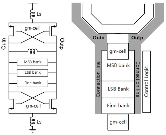
Figure 1.
The general CMOS complementary digitally controlled oscillator (DCO) architecture and layout.
The left side of Figure 1 shows a schematic of a DCO with three capacitor banks, i.e., the most significant bit (MSB) bank, the least significant bit (LSB) bank, and the fine bank. The largest switched capacitor is located near the main inductor for linear frequency change and chip area efficiency. In the layout of the DCO on the right side of Figure 1, the NMOS- and PMOS-type gm cells can be placed in either the tail of the capacitor bank or the neck of the inductor. The DCO located at the tail of the capacitor bank is the tail-DCO (TDCO) and the DCO located at the neck of the inductor is the neck-DCO (NDCO).
The LC resonant circuit is the key circuit that determines the oscillation frequency of the DCO, and consists of a main inductor and a bank of capacitors for frequency selection. The maximum frequency of the DCO is oscillated under the condition that all switches in the capacitor bank are turned off, and the minimum frequency is oscillated under the condition that all switches in the capacitor bank are turned on. Figure 2a shows the TDCO with the gm-cell circuit after the main inductor and capacitor banks. This creates an additional parasitic inductance between the main inductor and capacitor banks in the designed LC resonant circuit. As shown in Figure 2a, the maximum frequency shifts to a lower oscillation frequency under the condition that all switches are turned off by the added parasitic inductance. In the case of parasitic resistance and capacitance, ultra-thick metal (UTM) layers with small sheet resistance have small parasitic resistance values, and the parasitic capacitance is also ignored as a CMOS vertical structure between the ultra-thick metal (UTM) and substrate. Therefore, the tuning range of the oscillation frequency of the TDCO is reduced, and should be sufficiently considered in DCO design. However, the layout arrangement of the drive buffer can maintain symmetry with differential output signals.
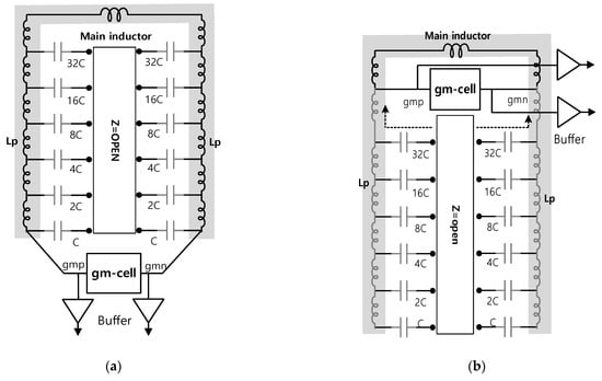
Figure 2.
Equivalent circuit of a DCO including parasitic line inductance (Lp): (a) gm cell is located in tail of the capacitor bank; (b) gm cell is located in the neck of the inductor.
Conversely, in Figure 2b, the gm-cell circuit of the NDCO is located in the middle of the main inductor and capacitor bank. This excludes the parasitic line inductance generated between the inductor and capacitor bank because all switches of the capacitor banks are turned off by high impedance. So, the DCO without parasitic line inductance has an oscillation frequency range with an LC resonant circuit, as designed. However, phase mismatch between differential signals can occur due to the asymmetry of the drive buffer connection.
2.2. Layout Method for High-Linear-Frequency Control
The high-frequency DCO is one sensitive circuits where oscillation frequency can be changed by parasitic components generated in the layout. In particular, the parasitic components of routing metal are some of the important design parameters to be considered in the DCO because it is difficult to design an LC resonance circuit that can be linearly adjusted according to the parasitic line inductance (Lp).
where Ls is the main inductor and Cvar and Cp are the capacitor and parasitic capacitance of the switching capacitor in the capacitor bank, respectively. Here, the ratio between the maximum frequency and the minimum frequency can be expressed as:
In Equation (4), the oscillation frequency of the DCO shifts according to the parasitic inductance. In addition, it has a nonlinear oscillation frequency due to the different parasitic inductances according to the position of the switches. The capacitor bank, including a linear capacitor unit, has a nonlinear oscillation frequency due to unexpected parasitic line inductance. As a method for minimizing the parasitic component of the routing metal, an ultra-thick metal (UTM) layer or Al metal layer commonly used metal options due to their low resistivity. In addition, a previous study [9] showed that using aluminum (Al) is a suitable method to reduce the parasitic inductance in LC resonance circuits.
For example, as shown in Figure 2a, the TDCO layout effectively reduced the parasitic inductance component using an Al metal layer. The capacitor bank circuit was covered by the Al metal layer to reduce the parasitic line inductance between the main inductor and the capacitor bank. It shortened the parasitic inductance, as shown in Figure 3. Capacitor banks, including short-circuit effects, have the desired oscillation frequency range due to parasitic inductance reduction. To verify this effect, we compared and verified the effect on reducing parasitic inductance by adding Al metal to the TDCO layout. For accurate parasitic extraction, an electromagnetic (EM) simulator can be used. However, this process requires a long simulation run-time and a complex setup. For accurate prediction of the results, implementation and simulation must be synchronized. Therefore, we compared the performance of the Al metal layer using actual fabrication and measurement without using EM simulation.
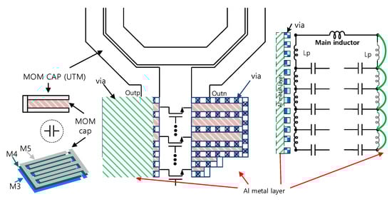
Figure 3.
Layout and equivalent circuit using a metal Al layer.
3. DCO Design
Figure 4 shows a simplified schematic with three capacitor banks, i.e., the MSB, LSB, and fine bank. All capacitor banks were designed with unit-weighted instead of binary-weighted structures to ensure linearity in the frequency step. Even though the area of the unit-weighted capacitor bank is slightly larger than that of the binary capacitor bank, it presents many merits in terms of linearity and flexibility in design [10]. For example, to change the capacitor required for linear oscillation frequency control, all unit capacitor sizes in the capacitor bank were changed, maintaining constant the ratios of capacitor sizes, such as unit ×1, ×2, ×4, and ×8 [10]. However, in the unit-weighted structure, the optimum capacitor unit value considering the parasitic components generated in the layout can be individually applied to optimize performance. For linearity and reliability, the unit capacitor contains inverter logic to bias the source and gate of the switch. Assuming a voltage swing (Vpp) of 0.8 at the output node and a supply voltage for the inverter logic of 1.2 V, when the switch was turned off, the turn-off-resistance of the switch was a few mega ohms, and the Vgs of the switch produced a voltage swing from −1.6 to −0.8 V based on the 1.2 V supply. Ensuring the Vgs reliability of a low-voltage threshold (LVT) switch with low turn-on resistance is difficult, therefore, a thick-oxide metal-oxide semiconductor FET (MOSFET) switch was used for the large signal swing of the DCO. However, the thick-oxide MOSFET switch increases the turn-on resistance and layout area, which complicates the design of the capacitor bank. To solve the reliability problem [8], if it is possible to supply a voltage lower than 1.2 V on the source voltage, an LVT switch with a low turn-on-resistance can be used. For this purpose, the supply voltage of the source inverter was 0.8 V, the same as the voltage of the DCO, and a different supply voltage from the inverter voltage for the gate was applied, as shown in Figure 4. This helped to improve the linearity and reliability of the DCO through a simple configuration power separation scheme. To reduce the mismatch between unit capacitors, the unit capacitor and control circuit should be arranged separately in the layout. This separation makes the arrangement conditions of all unit capacitors the same.
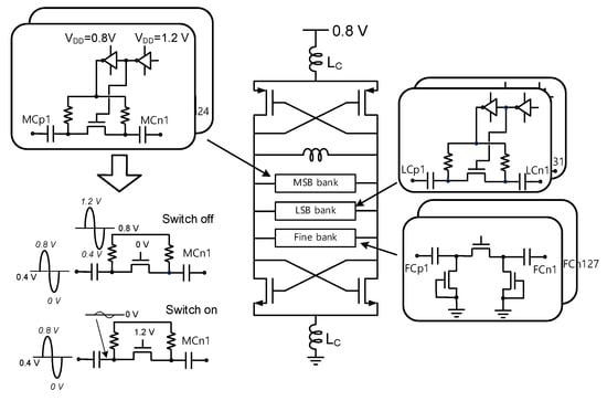
Figure 4.
Structure and operation principle of the switch and control circuit for tuning the capacitor in a capacitor bank.
Figure 5 depicts a useful method for reducing the mismatches between unit capacitors. In this design, the electrical control part and the unit capacitor cells were separated. The circles in Figure 5 represent a unit capacitor cell, which consisted of a switch, two capacitors, and two DC-blocking resistors. All these unit cells were located inside the capacitor dummy guard. The dummy was composed of unit cells that were the same size as those used for oscillation frequency tuning. This capacitor dummy layout was a layout technique for making all the coupling effects generated by the metal layer the same. In addition, the control logic blocks were located as far as possible outside the dummy for separation. When the electrically isolating layout was adopted, the randomness of the oscillation frequency was reduced, as shown in earlier studies of fabricated DCOs [8]. This layout method was applied to all capacitor banks, such as the MSB, LSB, and fine frequency tuning banks.
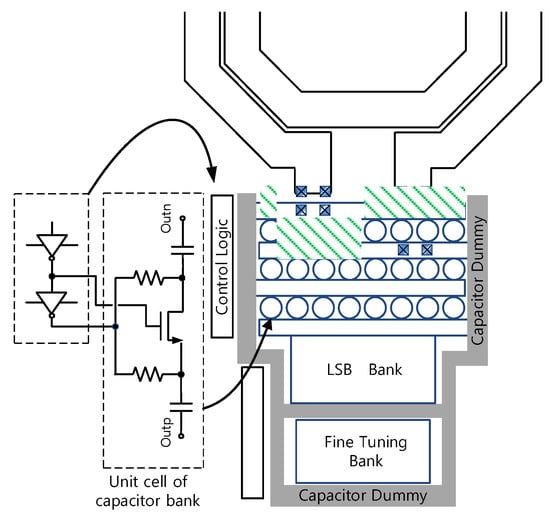
Figure 5.
Layout for high isolation between the unit capacitor cell and the control circuit.
4. Implementation and Measurement Results
To verify the effect of the proposed layout methods, three DCOs were implemented in then 55 nm CMOS process, as shown in Figure 6, and measured by a digitally controlled, embedded system. The DCOs were designed with the same inductor, capacitor banks, gm cell, and output buffers. The NDCO on the left of Figure 6 had a gm cell in the neck of inductor and the TDCO in the middle had a gm-cell in the tail of the capacitor bank. The Al-metal DCO (AlDCO) on the right of Figure 6 had a gm cell in the tail of the capacitor bank, which was applied to the Al metal layer for high linear frequency tuning.
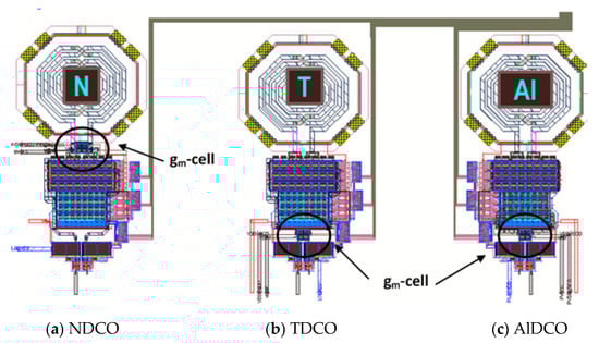
Figure 6.
The layout of the designed DCOs.
Figure 7 shows a chip picture of the designed DCOs. The NDCO and TDCO were designed with a layout area of 0.072 μm2 and the AlDCO with a layout area of 0.06 μm2, all integrated into one chip for comparison. For accurate performance comparison, the main inductor, capacitor bank, and gm cell in the DCO were used identically.
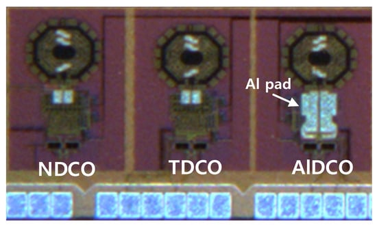
Figure 7.
The die photo of the designed DCOs.
Figure 8 shows the oscillation frequency range and the change in frequency according to the digital code. As shown in Figure 8a, the difference of measured maximum oscillation frequency was only 23 MHz between NDCO and TDCO. However, AlDCO presented a 347 MHz difference in maximum oscillation frequency compared to NDCO. The oscillation frequency range of NDCO and TDCO was about 923 MHz, and AlDCO was measured as having an oscillation frequency range of 775 MHz. Figure 8b shows the slope of the frequency according to the digital code. AlDCO showed a relatively linear frequency change compared to NDCO and TDCO, as expected, due to the additional Al layer. However, the maximum oscillation frequency was 148 MHz lower than that of other DCOs. In general, capacitor banks have small capacitor values at low digital codes. It becomes difficult to attain linear frequency control given the parasitic inductance of the layout. As shown in Figure 8b, the AlDCO produced a linear result at a relatively low digital code compared to the other DCO layouts. The results showed that the additional Al metal layer produced a linear frequency change effect but had a lower maximum frequency due to the parasitic capacitor generated between the capacitor banks. As such, when designing a DCO using an Al metal layer, a sufficient frequency margin should be considered.
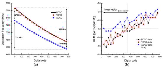
Figure 8.
Measurement of three test DCOs: (a) oscillation frequencies and (b) linear frequency control.
Figure 9 shows the phase noise of the designed NDCO at 4.8 GHz. The DCO exhibited low phase noise of −116.1 dBc/Hz at 1 MHz with a 0.8 V supply voltage. The overall performance of the DCOs can represented by a figure-of-merit (FoM) as follows [11]:
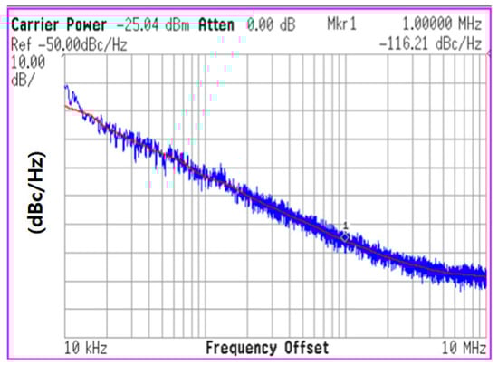
Figure 9.
Measurement result of phase noise in an NDCO.
The FoM of the designed NDCO was superior to that of the other DCOs. Since the NDCO had a gm cell in the neck of the inductor, the Q-factor of main inductor degraded less than that of the tail of the capacitor bank. The high Q-factor of the LC-tank resulted in the high performance of the NDCO.
Table 1 compares the performance of the measured DCOs, showing that the DCO consumed less power and had superior phase noise compared to existing designs, with a high FoM index.

Table 1.
Summary of performances of designed DCOs and comparison with previous works. FoM, figure-of-merit.
5. Conclusions
In this paper, the optimal gm cell position for the performance of the DCO and an Al metal layer for linear frequency control were implemented and compared using the 55 nm CMOS process. The fabricated DCOs presented different oscillation frequency ranges, phase noises, and power consumptions depending on their layout. According to the results, the DCO’s layout for BLE seems to be suitable for NDCOs, with the gm cell located at the neck of the inductor and a frequency tuning range of 17.8%, power consumption of 0.5 mW, and excellent noise performance of 116 dBc/Hz. For the TDCO, power consumption and phase noise of 0.58 mW and 114 dBc/Hz were recorded, respectively. The AlDCO for linear frequency control showed relatively poor performance, with 0.6 mW power consumption and 113.5 dBc/Hz phase noise, but showed a linear frequency change compared to the other DCOs.
Author Contributions
Conceptualization and writing—review and editing, M.-S.K.; writing—review and editing, S.-S.Y. All authors have read and agreed to the published version of the manuscript.
Funding
This research was funded by the Basic Science Research Program under Grant NRF-2018R1D1A1B07045432.
Informed Consent Statement
Informed consent was obtained from all subjects involved in the study.
Acknowledgments
The electronic design automation (EDA) tool was supported by the IC Design Education Center (IDEC), Korea.
Conflicts of Interest
The authors declare no conflict of interest.
References
- Gbadamosi, S.A.; Hancke, D.P.; Abu-Mahfouz, A.M. Building Upon NB-loT Networks: A Roadmap Towards 5G New Radio Networks. IEEE Access 2020, 8, 188641–188672. [Google Scholar] [CrossRef]
- Staszewski, R.B.; Leipold, D.; Muhammad, K.; Balsara, P.T. Digitally controlled oscillator (DCO)-based architecture for RF frequency synthesis in a deep-submicrometer CMOS process. IEEE Trans. Circuits Syst. II 2003, 50, 815–828. [Google Scholar] [CrossRef]
- Yoo, S.-S.; Choi, Y.-C.; Song, H.-J.; Park, S.-C.; Park, J.-H.; Yoo, H.-J. A 5.8-GHz high-frequency resolution digitally controlled oscillator for using the difference between inversion and accumulation mode capacitance of pMOS varactors. IEEE Trans. Microw. Theory Tech. 2011, 59, 375–382. [Google Scholar] [CrossRef]
- Wang, Z.; Wu, H.; Wang, X.; Shi, M.; Hu, S.; Guo, Y.; Cai, Z. A 0.5–0.7 V LC digitally controlled oscillator based on a Multi-Stage capacitance shrinking technique. MDPI Electron. 2019, 8, 1336. [Google Scholar] [CrossRef]
- Yao, C.-W.; Willson, A.L. A 2.8-3.2-GHz fractional-N digital PLL with ADC-assisted TDC and inductively coupled fine-tuning DCO. IEEE J. Solid-State Circuits 2013, 48, 698–710. [Google Scholar] [CrossRef]
- Issakov, V.; Wojnowski, M.; Knoblinger, G.; Fulde, M.; Pressel, K.; Sommer, G. A 5.9-to-7.8 GHz VCO in 65 nm CMOS using high-Q inductor in an embedded wafer level BGA package. IEEE MTT-S Int. Microw. Symp. Dig. 2011, 1–4. [Google Scholar] [CrossRef]
- Jhon, H.; Kim, M.; Kang, M. Cost-effective 4 GHz VCO using only miniature spirals realized in a 0.18 µm CMOS process for wireless sensor network (WSN) applications. MDPI Electron. 2019, 8, 1369. [Google Scholar] [CrossRef]
- Yoo, S.-S.; Lee, K.-Y. Design of 0.68-mW LC-based digitally controlled oscillator (DCO) for Bluetooth Low Energy (BLE) transceiver. J. Semicond. Technol. Sci. 2017, 17, 611–620. [Google Scholar] [CrossRef]
- Yao, C.-W.; Ni, R.; Lau, C.; Wu, W.; Godbole, K.; Zuo, Y.; Ko, S.; Kim, N.-S.; Han, S.; Jo, I.; et al. A 14-nm 0.14-ps rms fractional-N digital PLL with a 0.2-ps resolution ADC-assisted coarse/fine-conversion chopping TDC and TDC nonlinearity calibration. IEEE J. Solid-State Circuits 2017, 52, 3446–3457. [Google Scholar] [CrossRef]
- Hung, C.M.; Staszewski, R.B.; Barton, N.; Lee, M.C.; Leipold, D. A digitally controlled oscillator system for SAW-less transmitters in cellular handsets. IEEE J. Solid-State Circuits 2006, 41, 1160–1170. [Google Scholar] [CrossRef]
- Yoo, S.-S.; Lee, K.-Y.; Yoo, H.-J. Coupling-shielded inductor for high isolation between PA and LC-based DCO. IEEE Electron Device Lett. 2017, 38, 24–27. [Google Scholar] [CrossRef]
- Lin, Z.; Mak, P.; Martins, R.P. A 2.4 GHz ZigBee receiver exploiting an RF-to-BB-Current-Reuse Blixer+Hybrid filter topology in 65 nm CMOS. IEEE J. Solid-State Circuits 2014, 49, 1333–1344. [Google Scholar] [CrossRef]
- Roy, A.G.; Dey, S.; Goins, J.B.; Fiez, T.S.; Mayaram, K. 350 mV, 5 GHz class-D enhanced swing differential and quadrature VCOs in 65 nm CMOS. IEEE J. Solid-State Circuits 2015, 50, 1833–1847. [Google Scholar]
Publisher’s Note: MDPI stays neutral with regard to jurisdictional claims in published maps and institutional affiliations. |
© 2021 by the authors. Licensee MDPI, Basel, Switzerland. This article is an open access article distributed under the terms and conditions of the Creative Commons Attribution (CC BY) license (http://creativecommons.org/licenses/by/4.0/).