Article

Multiple Narrowband Interferences Characterization, Detection and Mitigation Using Simplified Welch Algorithm and Notch Filtering

LASSENA Laboratory, École de Technologies Supérieure (ÉTS), Montreal, QC H3C 1K3, Canada
*
Author to whom correspondence should be addressed.
Appl. Sci. 2021, 11(3), 1331; https://doi.org/10.3390/app11031331
Submission received: 11 January 2021 / Revised: 27 January 2021 / Accepted: 29 January 2021 / Published: 2 February 2021
(This article belongs to the Section Electrical, Electronics and Communications Engineering)

Abstract

:
By increasing the demand for radio frequency (RF) and access of hackers and spoofers to low price hardware and software defined radios (SDR), radio frequency interference (RFI) became a more frequent and serious problem. In order to increase the security of satellite communication (Satcom) and guarantee the quality of service (QoS) of end users, it is crucial to detect the RFI in the desired bandwidth and protect the receiver with a proper mitigation mechanism. Digital narrowband signals are so sensitive into the interference and because of their special power spectrum shape, it is hard to detect and eliminate the RFI from their bandwidth. Thus, a proper detector requires a high precision and smooth estimation of input signal power spectral density (PSD). By utilizing the presented power spectrum by the simplified Welch method, this article proposes a solid and effective algorithm that can find all necessary interference parameters in the frequency domain while targeting practical implantation for the embedded system with minimum complexity. The proposed detector can detect several multi narrowband interferences and estimate their center frequency, bandwidth, power, start, and end of each interference individually. To remove multiple interferences, a chain of several infinite impulse response (IIR) notch filters with multiplexers is proposed. To minimize damage to the original signal, the bandwidth of each notch is adjusted in a way that maximizes the received signal to noise ratio (SNR) by the receiver. Multiple carrier wave interferences (MCWI) is utilized as a jamming attack to the Digital Video Broadcasting-Satellite-Second Generation (DVB-S2) receiver and performance of a new detector and mitigation system is investigated and validated in both simulation and practical tests. Based on the obtained results, the proposed detector can detect a weak power interference down to −25 dB and track a hopping frequency interference with center frequency variation speed up to 3 kHz. Bit error ratio (BER) performance shows 3 dB improvement by utilizing new adaptive mitigation scenario compared to non-adaptive one. Finally, the protected DVB-S2 can receive the data with SNR close to the normal situation while it is under the attack of the MCWI jammer.

1. Introduction

Satellite communications (Satcom) are playing a crucial role in many applications, such as the global navigation satellite system (GNSS), direct broadcast satellite, and military/government services. Thus, it is necessary to guarantee the quality of service (QoS) and the security of end users [1]. High demand for radio frequency (RF) makes communications bands busier and closer together, making radio frequency interference (RFI) a more frequent problem. Insufficient out-of-band attenuation or overlapping spectrum from adjacent channels can cause adjacent channel interference (ACI) [2]. Interfered systems can face serious degradation in their performance or a complete cut off in data transceiving. A famous example of this modern wireless problem, is interference from Inmarsat that can completely stop Iridium uplink/downlink communications [3]. In many cases, the target of hackers and military forces is to prevent or corrupt RF communications. Jamming, is the intentional type of RFI transmitted in different wireless network layers [4,5]. Benefiting from recent advances in low-cost hardware and software-defined radios (SDR), jammers have more opportunity to deploy smarter jamming attacks to corrupt radio communication networks [6]. An inexpensive device can create a large variety of jamming signals; however, the mitigation process for the receiver is much harder [7]. On many applications, like navigation, partial or complete signal loss can have disastrous consequences thus, it is crucial to detect the RFI in desired bandwidth and protect the receiver with a proper mitigation mechanism.
Satcom channels suffer from several destructive effects like Doppler [8] and variable time delay [9]. In a typical digital receiver, a chain of several blocks is employed to compensate the channel effects and fulfill the demodulation duty. The complete data reception depends on efficient performance of all of the blocks and if one block cannot fulfill its duty, all the packet data will be lost. In the presence of interference, it is more complicated for signal processing blocks to complete their duties. There are several sensitive blocks in a digital receiver that can be disrupted by even a low power interference. Thus, damage to digital receivers varies from complete packet lost to error increment and QoS reduction [10].
Before the reception chain, the mitigation stage tries to remove the interference while preserving the useful part of the desired signal as much as possible; however, suppressing the interference with minimum damage to the system performance is a very complicated task. Usually, before the mitigation block, a detector tries to accurately characterize and recognize the interference properties [11]. The type, the center frequency, and the bandwidth are common extracted features. After that, the mitigation mechanism is adaptively adjusted for optimum interference cancelation. Thus, generally speaking, the protective box before the receiver chain has two main sub-blocks [12]: the detector and the mitigation block. Structure of these two blocks changes depending on the type of the signal of interest (SoF) and the interference type.
Fortunately, some systems already exist to mitigate the negative effects of those RFIs. Especially for the GNSS signals, different methods are designed to detect and suppress interferences [12,13]. Since the GNSS signals are wideband signals, it is easier to detect and suppress interference because the noise and power level are lower than narrowband interference. For this type of receiver, higher jamming to noise ratio (JNR) makes the interference easier to detect [14].
Compared to GNSS signals, which interferences are located on the top of the flat and wideband noise, with a modulated-narrowband signal such as a Digital Video Broadcasting-Satellite-Second Generation (DVB-S2) standard [15], the amplitude level of the signal is much higher than the noise. This research mainly focuses on modulated-narrowband digital communication signals. In a digital transmitter, output bit stream of data source first is mapped into two-dimensional space by the help of constellation modulator. A constellation diagram, such as phase-shift keying (PSK) or quadrature amplitude modulation (QAM), represents the signal as a two-dimensional diagram; however, such a baseband signal is ideal and has a spectrum with very low sidelobe decay rate that does not fit its frequency bandwidth. Thus, it is necessary to limit the effective bandwidth by the help of pulse shaping. Usually, pulse shaping uses raised-cosine filter due to its ability to minimize intersymbol interference (ISI) [15]. Visible interference part is located on the top of the signal power spectrum, thus the existing algorithm used for interference detection in a wideband signal does not work directly with a narrowband signal. Instead of JNR that compares power level of noise with interference power, the jamming to signal ration (JSR) that compares the signal power with interference power must be utilized. Figure 1 displays the visibility of the continuous wave interference (CWI) in different conditions for a modulated signal (narrowband). Target of figure one is to compare effect of JSR and signal to noise ratio (SNR) on detection performance. In Figure 1a, multiple carrier wave interferences (MCWI) with different JSRs is added to the modulated signal. Variation in JSR has an impressive effect on the amplitude of the CWI on top of original signal. Figure 1b tries to explain the effect of different SNRs on clarity of interference, thus the parameters of interference (center and power) are constant and additive white Gaussian noise (AWGN) with variable SNRs is added to the transmitted signal and then CWI (with fixed JSR) is added to the noisy signal. The same interference is utilized with different SNR level, thus only one peak is observed in Figure 1b. As it can be seen, for smaller SNR, the level of noise raises; however, it does not affect the position and visibility of the CWI peaks compared to the power level of the signal. It can be concluded that the main effective parameter in interference detection is JSR, thus the accuracy and precision of a detection algorithm must be based on the input JSR of designed detector.
This study proposes a novel detector and mitigation mechanism for the protection of the narrowband-modulated signal. Digital receiver blocks and their performance are sensitive to the low power interferences. Thus, this study tries to extract a high quality power spectrum and utilize it to estimate the important characteristics of multi-interferences with high resolution and precision. One of the most important targets of this research is to propose a design that can fit in small and common receivers. Thus, all designs are based on simple and basic logical elements that can be found in the field-programmable get array (FPGA) design libraries. Such practical design can be implemented in almost all software environments or embedded in small area of FPGAs with a very low complexity. The proposed design is based on simple blocks, but it is smart and efficient to extract several interference parameters and utilize them for adaptive adjustment of mitigation block. In the heart of the detector, the simplified Welch method is employed for smooth and flexible power spectral density (PSD) estimation. The simplified Welch method [16] gives a smooth PSD where its SNR is enhanced with the help of weighted averaging. Based on the current situation demand, by simply changing one feedback parameter and without any hardware change, the detector can change its mode from a very low power interference detection to hopping center frequency detection. Proposed detector can detect several multi narrowband interferences and estimate their center frequency, bandwidth, power, start, and end of each interference individually. To remove multiple interferences, a chain of several IIR notch filters [13] with multiplexers is proposed. The detector can employ notch filters as much as required, which is equal to the number of observed interferences. Because a narrowband modulated signal carries a lot of information in a dense bandwidth, interference mitigation must be fulfilled with minimum damage to the original signal. The bandwidth of each notch is adjusted in a way that maximizes the received SNR by the receiver. MCWI is utilized as a jamming attack to the DVB-S2 receiver and performance of the new detector and mitigation system is investigated and validated in MCWI detection/mitigation with both simulation and practical tests.
The structure of the paper is organized as follows: Section 2 reviews the previous research in RFI detection and mitigation. The methodology, detector structure, and mitigation scenario are proposed in Section 3. The demonstrated simulation results are presented in Section 4. Test bench set up for practical and real-time test are presented in Section 5. Moreover, this chapter explains the obtained results from practical tests with the DVB-S2 receiver under the attack of the MCWI jammer.

2. Literature Review

Besides the design of protection systems for Satcom communication, it is also necessary to study the interfered system under jamming situation and also the effect of the mitigation in performance enhancement or QoS degradation [17]. Study [10] depictures inside the body of a typical receiver with details and shows the reaction of the essential digital receiver blocks under RFI situation. The study proves that in an attack, not only the power of interference, but also its center frequency plays an important role in system corruption. It is shown that, a smart and low power jammer with a center close to the Doppler value can completely stop the receiver. Moreover, it is shown that even if a low power CWI does not stop the receiver, it still decreases the QoS and affects the SNR and bit error rate (BER) significantly. Thus, it is crucial to design a detector with the capability of very low power detection for this type of receiver. Because a narrowband modulated signal carries a lot of information in a dense band, the mitigation step must also be fulfilled very carefully. A notch filter is proposed as a computationally efficient solution for protecting the system against narrowband attacks. Several criteria like SNR measurement before and after filtering are proposed for optimum adjustment of the notch filter bandwidth. However, center frequency estimation and bandwidth adjustment based on the RFI power is postponed to future works.
Prior to this study, several protection methods for Satcom communication have been researched. Artificial intelligence techniques is an emerging topic for RFI detection and characterization [18]. Research [1] extracts different features from the input signal and utilizes them as the input for machine learning (ML) and multi-layer perceptron (MLP) for RFI recognition and automatic classification. Based on the results, MLP is able to classify RFI in three categories CWI, MCWI, and Chirp with robust and high precision. Artificial intelligence is able to classify the mixed interference in one of the narrowband, multi-narrowband, or wideband. Knowledge about the input type can be considered as the first step in RFI characterization. It helps the detector to utilize the proper method and extract the necessary information about RFI easier and with more accuracy.
In a general view, the detector tries to estimate the center frequency and power of interference with maximum accuracy in different ways. Detection methods can be divided in three categories: temporal domain, frequency domain monitoring, and spatial domain detection techniques [12]. Time domain algorithms like least mean square (LMS) [19] and recursive least square (RLS) [20] recursively converge to the center frequency of the narrowband interference. The LMS method is used vastly for narrow band interference detection in GNSS systems. The main advantage of the LMS algorithm is its simplicity. As discussed earlier, the structure of the modulated signal power spectrum is completely different from the GNSS signal and that makes the detection of CWI more complicated. Time domain detectors are more sensitive to the noise and they are not suitable for weak interference mixed with modulated signals because of their special power spectrum shape. Compared to the time domain algorithms, second class of detectors transfers a window of input samples into frequency [21] or wavelet domain [22] and tries to analyze abnormalities in samples and characterize them as interferences. In [23], wavelet-packet-transform is utilized to detect and mitigate the powerful CWI and Chirp jamming. The fast Fourier transform (FFT), which is an efficient computational version of the DFT, is commonly used to present the signal in the frequency domain [24]. The squared amplitude of FFT samples represents the first estimation of power spectrum distribution in the frequency domain. It is common to compare the power spectrum (or Wavelet) samples with a dynamic threshold and consider larger samples as the interference [17,23,25]. The main issue with simple FFT is that frequency samples are calculated just based on one window of the data stream, which makes the estimated power spectrum noisy with less precision. Such detectors are suitable for powerful interference detection not for weak power RFIs. The Welch method can enhance PSD estimation with arithmetic averaging over several FFT packets [26]. However, complexity and required random access memory (RAM) for saving the previous FFT packets increase by the number of involved FFT packets in averaging. The complexity limits the hardware implementation of the Welch method. Another issue happens when the system needs to track hopping interference, in this case, Welch method does not have enough flexibility to support the detector.
Smaller and end user devices also need to have access to a high-quality spectrum and a fixable detector. Most of the available detectors use complex algorithms and circuitry to protect an especial application against a type of interference. It mostly results in an expensive and heavy device which may be unpractical for smaller devices and complex to implement. The recently simplified Welch method [16] is introduced as a promising candidate for enhanced PSD estimation. Benefiting from simple and practical design, it can convert an academic SDR to a worthy spectrum analyzer. It gives the end user flexibility to adjust the degree of averaging by simply tuning one feedback level. Thus, it motivates us to design a new detector based on that algorithm.
IIR notch filters are widely used with mitigation systems to protect different communication protocols like wireless local area network (WLAN) standard (IEEE 802.11a/g/n/ac) [27,28], GNSS [13], and discrete multi-tone (DMT) system [29,30]. There is a tradeoff between the remaining interference power and removed data from the spectrum of the desired signal. When the interference power is low, the important parameter is the removed frequency band from the desired spectrum. While for powerful interference, residual interference is more important and can paralyze special blocks in the chain block of the receiver. After mitigation, performance enhancement is explained as BER improvement. Mentioned algorithms can improve performance compared to the unprotected system; however, for a narrowband modulated signal, QoS is more sensitive to spectrum manipulation and solid criteria must be used for notch filter bandwidth adjustment [10].
The current article tries to cover the shortcoming in the research area by deploying the following points:
  • As the main element of spectrum monitoring and detection, a smooth and flexible PSD is extracted from the input signal based on the simplified Welch method [16]. Flexibility of this method allows the detector to tune the PSD smoothness from the degree equivalent to 100 averaging of previous FFT packet to a simple FFT. In this way, the detector can change its mode from very low power interference detection to low power interference with hopping center frequency detection.
  • By the smart design based on the basic logic elements, the proposed detector can extract necessary information about the mixed RFI in the desired signal: (1) grouping the abnormality points in PSD as individual interferences and gives the number of required notch filter; (2) Start, end, center, and bandwidth of each interference; (3) Power of each interference.
  • A criterion based on the interference power (JSR) and optimum reception SNR is proposed for notch filter bandwidth adjustment.
  • By mixing the chain of notch filters with the multiplexer, the variable number of notch filters can be activated equal to the detected number of interferences. It minimizes removed useful information from signal spectrum.

3. Methodology and Solution

3.1. General Solution

In this section, a detailed structure of the detector and interference mitigation system is presented. Figure 2 displays the proposed design based on downsampling and notch filtering. Based on this structure, the input signal passes through two different paths. The first path directly goes to the chain of adaptive notch filters, which their center frequencies and bandwidths are adjusted by the detector. This paper focuses on the narrowband digital communication signals. Usually in a digital receiver, an analog to digital converter (AD) samples the input RF signal with a sample rate several time faster than the largest maximum frequency component. A faster sample rate is necessary for fulfilling the symbol time recovery (STR), which extracts symbols with maximum power from input samples [9]. Thus, as it can be seen in Figure 1, the desired signal power spectrum is located in a narrow bandwidth of all frequency interval. The target is to detect and remove the in-band interferences. In this way, the detector does not need to investigate all frequency bandwidth and by zooming on the useful interval, it can obtain better and more accurate results. One of the common ways for zooming in frequency domain is downsampling. To avoid aliasing before downsampling, the input signal is passed through a low-pass filter, which removes the extra bandwidth and avoids folding [31]. The downsampling rate must be chosen based on the signal bandwidth and sample rate of analog to the digital converter of the receiver. Consider that AD samples the RF signal with sample rate F s and input signal has the maximum bandwidth B W . Based on the Nyquist theorem, maximum downsampling factor must be smaller than F s B W .
After downsampling, the signal passes through the detector itself to extract the main characteristic of each interference and carry this information over to the filters. In the frequency domain, an effective narrowband interference can be considered as an abnormality on top of the desired signal spectrum power. One can describe this abnormality with three main factors: center frequency, bandwidth, and power. The main job of the detector bank is to group the abnormalities as individual interferences and estimate these three parameters for each detected interference. An adaptive notch filter is a band-stop filter where its center frequency and its bandwidth are adjustable based on the situation. Detector bank estimates the characteristics of each interference and adjusts the center and bandwidth of each notch for optimum quality of service (QoS).
Notch filter also removes a part of the useful spectrum of the signal, thus it is necessary to activate the mitigation system when the interference is detected and remove the notch filter from the receiving chain when there is no interference. In other words, the number of utilized notch filters must be equal to the observed interferences. The detector handles this important duty with the help of the multiplexer. Each multiplexer has two inputs: the signal that passed through to the last notch and the signal that does not go to the notch. Based on the selection process, the detector selects one of these two signals by the help of the “select” signal. When all “select” pins are zero, no filtering is applied to the input signal. This helps to have several notches in the chain of the receiver and utilize as much as required based on the current situation.
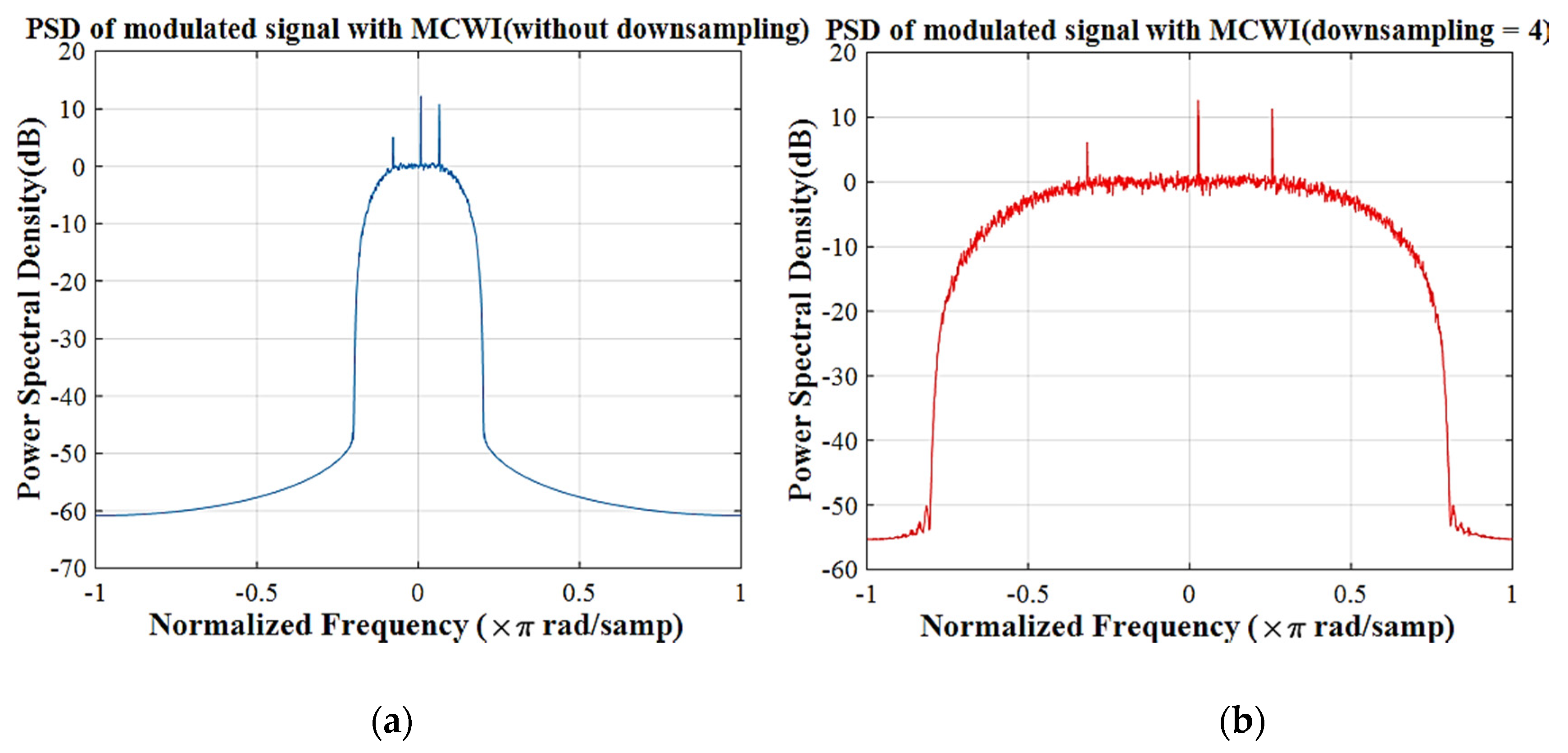
The high-power level of the modulated signal makes the detection process difficult; however, for a narrowband signal, when the interference center frequency is out of the interest bandwidth, it cannot affect the receiver’s performance. In other words, if a detection algorithm tries to find the interference in the entirety of the interval [−π π], its efficiency will be negatively impacted. The easiest way to increase the resolution in the frequency domain is to downsample the input signal before detection. If we ignore the two boundaries of power spectrum in Figure 3b, after downsampling, the power spectrum is more similar to an interference on top of flat noise. This flattened shape allows the system to benefit from the designed detector for the GNSS signal.
Figure 3a,b try to explain improvement in focusing and resolution by the help of downsampling. As an example, three CWIs with different powers are utilized as interference. Based on this comparison, after downsampling by the right factor (M = 4), the area of interest is zoomed-in and that increases the resolution of the detector. Considering that the detected center frequency of the CWI is downsampled equal to f interference   d o w n   s a m p l e d   , then the center frequency of interference can be easily expressed as:
f interference = 1 M · f interference   d o w n   s a m p l e d   .
If a detector transfers a window of time domain samples to the frequency domain by FFT with size N F F T , the resolution between two frequency samples is equal to the 1 N F F T . Based on Equation (1), after downsampling, the resolution will improve to 1 M   ×   N F F T .
Downsampling can improve the detector performance in both resolution and capability in the weak signal detection; however, it increases the required samples number for correct detection. Consider that the detector needs N samples to reach convergence or to fulfill its duty, after downsampling by a factor M, the input of the detector now requires N × M samples. The time of detection is now multiplied directly by M. Thus, the direct drawback of downsampling is that the convergence time to the correct estimation is multiplied by M factor.

3.2. Detector Bank Based on Simplified Welch Algorithm

As mentioned above, one of the goals of this paper is to propose a new detection method using the simplified Welch algorithm [16]. The detector uses the power spectrum samples and their indexes to detect and characterize multi interferences or unusual behaviors in the spectrum of the signal. Proposed detector can estimate the following parameters (Figure 4):
  • Number of interferences;
  • Center frequency of each interference;
  • Power of each interference;
  • Bandwidth of each interference.
The target of this section is to present a solid and smart algorithm that can find all the above parameters in the frequency domain while targeting practical implantation for embedded system with minimum complexity. In this system, downsampling is used before the simplified Welch’s algorithm to have more precision and capability for weak signal detection. As it can be seen in Figure 4, detector structure contains three main blocks:
  • Simplified Welch algorithm: this block extracts the PSD samples from the input data stream.
  • Thresholding activator: this block compares PSD samples with a threshold level and for each group of abnormality on the top of PSD, generates a pulse that activates a detector.
  • Detector bank: contains N detectors that each one is activated by the enable pulse from thresholding activator. Each detector extracts and saves the characteristics of an interference.
It should be mentioned that, any PSD estimation method, like original Welch method, can be utilized to estimate in the proposed detector. In the following sections, each part is explained with more detail.

3.2.1. Welch and Simplified Welch Method

To scan the signal in the frequency domain, frequency samples are extracted from the input signal by the help of FFT [24], which is a much faster computational implementation than the discrete Fourier transform:
X [ k ] =   n = 0 N 1 x [ n ] e j 2 π n k / N   0   k   N 1 ,
where N is the number of input samples, k is an integer index, 2 π / N   is the fundamental frequency resolution, x =   { x [ 0 ] , x [ 1 ] , x [ n ] }   is the window of input samples, and X =   { X [ 0 ] , X [ 1 ] , X [ n ] } is the vector of DFT samples. This method is widely used, but the problem is the ambient noise and limitation due to the finite number of samples in the input window. The Welch samples are an estimation of the power spectral density based on the arithmetic average of multiple squared amplitude of FFT scans. The Welch algorithm uses averaging (or arithmetic averaging) in order to achieve two important goals:
  • SNR improvement: averaging over more samples can reduce the noise power level and enhance the SNR of desired signal.
  • Precise estimation: by utilizing FFT samples from the past, each frequency component can be estimated with more precision and it makes the frequency spectrum smoother than the raw FFT output.
Let us consider that the FFT is calculated over the entire duration of the signal. In the Welch algorithm, instead of processing the FFT over the entire time domain, the signal is separated in windows with the same size. Consider that the input vector signal s contains the N samples [32]:
s = x [ 1 ] ,   x [ 2 ] ,   ,   x [ N ] .
The signal can be separated in K smaller intervals with M length and V overlapping:
1 : s 1 = x [ 1 ] ,   x [ 2 ] ,   ,   x [ M ] 2 : s 2 = x [ M V + 1 ] ,   x [ M V + 2 ] ,   ,   x [ 2 M V ] K   : s K = x [ ( K 1 ) M ( K 1 ) V + 1 ] ,   ,   x [ K M ( K 1 ) V ] ,
where s i =   { s i [ 1 ] , s i [ 2 ] ,   s i [ M ] } represents the ith window, and K is number of the involved window in the PSD calculation. The DFT is calculated for each window:
S i [ v ] =   m = 1 M s 1 [ m ] · w [ m ] exp ( 2 π j m v N F )     1 v N F ,
where w =   { w [ 1 ] , w [ 2 ] , w [ M ] } is the windowing vector, NF is the DFT size, and   S i =   { S i [ 1 ] , S i [ 2 ] ,   S i [ N F ] } represent the vector of frequency samples of ith input window. Periodogram values are squared of the absolute value of the DFT samples:
P i [ v ] =   1 C   | S i [ v ] | 2   1 v N F ,
where C is normalization factor:
C = m = 1 M w 2 [ m ] .
Calculated periodogram values from different windows are averaged and the power spectral density estimate is obtained:
P S D [ v ] =   1 K i = 1 K P i [ v ]   1 v N F ,
where the K is the arithmetic averaging order. We have samples of K intervals, then we obtain K amplitude of FFTs and then calculate average of them to reduce the noise. However, arithmetic average of past samples have the following consequences:
  • Implementing arithmetic averaging of N order requires N random access memory (RAM) components and massively increases the complexity for real-time implementation.
  • All the previous samples are weighted by the same coefficient. For example, the sample with a distance of 10 times the intervals from the current sample is weighted by the same gain as the sample with a distance of 100 times the intervals. However, in many systems, it is suitable to weight the samples based on their distance from current samples.
Recently, a simple solution with the help of RAM was presented to calculate Welch samples based on the weighted averaging [16]. The ability of this design to clearly display low-power interference on top of a noisy signal is very promising for the detector. In this method, arithmetic averaging is replaced by the recursive geometric series. For ith input window, PSD samples are calculated as the following equation:
P S D i [ v ]   =   α × P S D i 1 [ v ] +   P i [ v ]   a n d   0 α < 1 .
As it can be seen, calculated PSD depends on the weighted pervious PSD and current amplitude of the frequency samples. The α parameter determines the dependency on the past, with a larger α , more PSDs from the past are involved in the calculation and a smoother power spectrum is obtained. Smaller α results in faster convergence, but rougher estimation of the spectral density. The proposed simplified Welch algorithm has a structure that completely fits the Xilinx DSP generator library and can be easily implemented as a real-time PSD estimator. This method generates the PSD samples in series manner and synchronizes the start and end of each vector by the help of “Data Ready” pulse. After estimation of N F PSD samples, a data ready pulse is generated to synchronize all PSD packets.

3.2.2. Thresholding Activator

In the heart of the design, there is a thresholder that is connected to a counter that counts on the rising edges (Figure 5 and Figure 6). This block handles the job of grouping the observed abnormalities into the separated interferences. Consider that the detector wants to group the PSD samples in the frequency interval [ f 1   f 2 ] as interference number one and samples in the frequency interval [ f 3   f 4 ] as interference number two. Based on Figure 5 and Figure 6, the thresholder generates separated pulse for each interference:
G e n e r a t e d   P u l s e ( v ) =   { 1   i f   P S D ( v ) T l 0   i f   P S D ( v ) < T l } ,
where T l is the selected threshold level. The threshold level can be adjusted based on the desired signal static during the initialization or an interval that the receiver receives the signal without the interference. One of the good candidates is the average of the maximum point of normalized power spectrum. Another option is the average of the top level of the observed PSD. Usually, inside the digital receiver, there is an automatic gain control that maintains a suitable signal amplitude at its output. To be sure that the thresholder is working correctly, all the input data streaming to the detector can be normalized to unique power.
On the rising edge, the counter counts one number up. It should be mentioned that the data ready pulse from the power spectrum estimator resets the counter for each vector of PSD samples. The output number of the counter is compared to the series of numbers from one to N (Number of detectors). After a logical AND with the output of the thresholder, the activator signals are ready. The main duty of this block is to generate separated pulses for each interference with the correct time interval for activating each detector. When a detector is activated at the correct time, next steps can be done easily. The output of the counter displays the number of abnormalities above the threshold level and the number of notch filters that must be activated to remove the interferences.

3.2.3. Detector Bank

Parameters of each interferences must be extracted and saved separately, a “Detector Bank” is used to achieve this target. The number of detector blocks is not limited and one can add detectors as required to the design (Figure 7). However, after completing the design and synthesizing, the maximum number of detected interferences is limited to the number of embedded detectors. For instance, if the design is equipped with three detectors, then the system is capable to detect a maximum of three interferences. As it can be seen, this block has four inputs: enable pulse, estimated amplitude of power spectrum, index of spectrum samples, and data ready pulse.
Now, let us look at the next stage to extract the characteristics of each interferences (Figure 7). The previous block makes the system capable of extracting the pulse that determines the start, end, and the interval of each interference. This pulse is utilized in Figure 7 to extract all desired parameters. There are two registers that work with the rising and falling edge. The rising edge register saves the start frequency of interferences f 1 and the falling edge register saves the end frequency of interference. The accumulator works with the activator signal level. During the time interval that enables, the signal is high, the accumulator gathers the values of the estimated spectrum samples. This accumulation simply calculates the v P S D ( v ) , which is the main parameter for average power calculation. There is also a counter in each detector that counts from zero to one when it receives the activating pulse. The output of this counter is utilized as the “select” signal for multiplexer. When there is no activation pulse, the counter is reset to zero by the data ready pulse and related notch filter is removed by the multiplexer from the reception chain.
The last layer of registers helps the system to save the extracted characteristic of interference and update them for each estimated packet of PSD.

3.3. Multi Mitigation Using the Chain of Notch Filters

In order to remove the interference, a chain of notch filters is utilized. A notch filter is a narrow stop band filter that removes a very small section of the original signal at a very specific frequency band. The role of the notch filter is to remove the interference while keeping as much as possible of the valuable data. The transfer function of the IIR M-order notch filter can be expressed as [33]:
H ( z ) =   i = 1 M 1 ( 1 e j ω i z 1 ) i = 0 M 1 ( 1 r e j ω i z 1 ) ,
where   ω i represents the center frequency of each notch and the pole radius r ( 0 < r < 1 ) controls the bandwidth of each notch. One important note about DVB or other communication signals is that, information is carried in two dimensional In-phase and Quadrature components. It means that these signals can be considered as complex signals. By replacing M with 1, the Equation (11) can be simplified as the first order complex notch filter:
H ( z ) =   1 e j ω 0 z 1 1 r e j ω 0 z 1 ,
where w 0 is the center frequency of the notch filter. As it can be seen, each notch filter is controlled by two parameters: w 0 as the center frequency and r that determines the gap bandwidth (Figure 8). Using this notch filter design, paired with the detector presented above, the interference mitigation system can adaptively track and remove narrowband interferences from the original signal.

3.4. Adaptive Bandwidth Adjustment for Notch Filter

As previously discussed, a notch filter is an adjustable gap in the frequency domain. That gap center frequency and bandwidth are controlled by two parameters:   f c   and r . The proposed interference detector has two main capabilities: center frequency estimation and interference power calculation. Detected center frequency can directly be utilized to adjust the center of the gap of the notch filter on narrowband interference. However, filter bandwidth adjusting is more complicated and demands a careful study about the SNR based on the r parameter after filtering. It should be considered that the filter also removes a part of the useful received signal. Clearly, interference cancelation for powerful interference demands a wider gap or a greater attenuation from the notch in the frequency domain, but there is a tradeoff between the amount of interference power reduction and the removed bandwidth from the signal.
To study the effects of bandwidth removal on the system’s performance, a study based on Figure 9 is done to calculate the optimum r parameter based on the input JSR. The target of this process is to generate a general modulated telecommunication signal with pulse shaping. After the signal generator, a CWI interference with variable power is added to the desired signal. In the receiver, a notch filter tries to remove the interference. Then, the system performance is measured with the SNR measurement between the transmitted signal S t and final signal after filtering S f   [34]:
S N R =   v a r ( S t ) v a r ( S t S f ) ,
where v a r ( S t ) =   i = 1 K ( S t [ k ] u ) 2 K denotes the variance of S t and u is the mean value of S t . The r parameter must be adjusted in a way that the interference is removed completely from the desired signal with a minimum amount of useful signal being removed from the original signal. In other words, the notch filter must remove the interference completely with the minimum available bandwidth to preserve the quality of service. CWI decreases the received SNR and notch filter tries to remove the interference power by generating a gap at the position of interference and decrease its power. Decreasing interference power increases SNR. r parameter adjusts the notch bandwidth and it can vary between 0 < r < 1 . Selecting the notch bandwidth (or r parameter) affects the SNR improvement:
  • If notch bandwidth is small, interference power is not completely removed.
  • If notch bandwidth is larger than enough, the interference power is removed but the extra useful spectrum of signal is also removed.
Both mentioned cases cause that the SNR does not achieve its maximum. The optimum r adjusts the notch bandwidth in the way that interference power is mitigated and the minimum bandwidth of the spectrum is removed or in another words, we must adjust the notch gap in the way that the maximum SNR after filtering is obtained:
r o p t i m u m = A r g   max r ( S N R )   ,   0 < r < 1 .
Equation (14) expresses that the value of r that maximizes the received SNR after filtering is the optimum selection. Utilizing optimum r will maximize the SNR value in Figure 9.
Figure 10a displays the output SNR of the notch filter based on the notch bandwidth (r parameter) for different CWI powers (JSR parameter). It can be seen that, for a special JSR (interference power) value, the output SNR peaks at a special r parameter value that is optimal for that JSR. Based on these figures, when the JSR is large, there is a powerful peak on top of the desired spectrum and a notch filter with a larger gap is required to completely remove all interference power. On the other side, when the JSR is small, a notch filter with a smaller gap must be utilized to preserve the spectrum quality as much as possible. If the utilized notch filter is smaller than the optimum r, residual power of interference will decrease the received SNR and if the gap bandwidth is larger than what is required, the unnecessary spectrum from the input signal will be removed and that will decrease the SNR of the system. Figure 10b displays the optimum r parameter value based on the input JSR that maximizes the SNR in the receiver. Based on this figure, the mitigation stage can adaptively adjust the r parameter based on the input JSR.
One may ask this question: “How can the detection system estimate the input JSR?” The answer is: The detector is also capable of the interference power measurement. Based on the proposed structure for the detector bank, the detector can simply estimate the power and its average. Figure 11 displays the input JSR based on the measured interference power in the detector. These two figures are references for adaptive notch filtering and can be simply saved inside the software (or FPGA) as a look up table and be utilized as the reference for adaptive r adjustment.

4. Simulation Results

4.1. Detection Results

As discussed above, JSR is the most effective parameter in the detection process. Ideal detectors must be able to detect very low power CWI; however, the capability and precision of the detector depends on the downsampling factor, input signal type, interference characters, and adjusted parameter for the detector. The precision of the detected center frequency directly affects the efficiency of notch filters in CWI mitigation. When the mitigation stage has a precise estimation of CWI center frequency, a narrow notch filter can be utilized for interference cancelation. When the notch filter deviates from the exact center frequency, interference power will leak to the receiver, the notch must then utilize a wider notch for complete removal. The following condition helps to measure the detector precision:
i f   ( | f d e t e c t e d f i n t e r f e r e n c e     | > ε T )   I n c o r r e c t   D e t e c t i o n i f   ( | f d e t e c t e d f i n t e r f e r e n c e     | ε T )   C o r r e c t   D e t e c t i o n ,
where f d e t e c t e d is the detected center frequency by the detector, f i n t e r f e r e n c e     is the real center of interference, and ε T is the desired precision: if the detector deviates more than this value, its detection is not acceptable. Table 1 displays utilized parameters for simulation tests.
For the comparison target, performance of the detector with the original Welch power spectrum estimation is also presented. Figure 12 displays the percentage of correct detection based on the input JSR. Minimum detectable JSR for the original Welch algorithm depends on two important factors: number of involved FFT packets in arithmetic average (averaging order) and downsampling factor. Clearly, by increasing the average order, more FFT packets are involved in PSD estimation and as the result, the system with a higher order has an outstanding result in precise center detection. When the system benefits from the average of 80 past FFT packets, it detects weak power CWI with JSR = −22 dB. It can be seen that increasing the downsampling factor from two to four, approximately increases the system performance by 3 dB.
System performance of the simplified Welch algorithm is controlled by the α parameter. Compared to the original Welch method, α parameter plays the same role as the averaging order. By increasing α parameter, the estimated spectrum has more dependency on past calculated frequency samples and is smoother and more accurate. Based on Figure 13, changing the α parameter can improve the detector system performance in weak signal detection to the JSR = −25 dB. Downsampling again plays the same role and by increasing down sapling factor from two to four, a 3 dB improvement is observed in system performance. It can be seen that detector with 𝛼   = 0.99 can excel the original Welch that benefits from averaging of 80 previous packets.
As it is mentioned before, benefiting from the averaging, the proposed design has a unique capability in weak signal detection. Machine learning and artificial intelligence techniques are able to classify the type of interference and they cannot estimate the center frequency. The utilized algorithm in [1] is capable of classifying the interference with JSR larger than 5 dB. As an example of time domain algorithm, Figure 14 displays the performance of the LMS algorithm [19] in CWI detection mixed with the narrowband signal. After downsampling by factor 4, this algorithm can detect the interference down to JSR = −6 dB. The wavelet algorithm is mainly used to detect the interferences with JSR between 10 to 55 dB [22,23].
Based on the previous results, utilizing more packets from the past increases the system capability in weak interference detection; however, the cost of this improvement is more convergence time and slower reaction to interferences with the variable center frequencies. Consider that the target of the system is to track the interference with hopping center frequency. Depending on the variation speed of center frequency, large dependency on the past can decrease the system performance. Let us consider that the sample rate of the system is large enough and during one FFT window, the interference has a constant center frequency. Now, the period of the variation of interference center frequency is an integer multiply of window duration. For simplicity, we normalize a window duration to one second. Figure 15 displays the detector performance in hopping CWI tracking based on the variation speed of the center frequency. In this test, the power of interference is constant (JSR = −15 dB and downsampling = 2). Clearly, the detector with large dependency on the past (larger α parameter) is not able to track the fast variations in signal PSD. In this case, the α parameter must be selected carefully. The amount of dependency must be large enough to make the interference visible but it must not filter the fast variation of center frequency hopping. By comparing Figure 13a and Figure 15, detector behavior can be explained. In Figure 13a, at JSR = −15 dB, the detector has a detection rate = {71%, 90%, 98%, and 100%}, respectively, for 𝛼 =   { 0.6   0.7   0.8   0.9 } . For 𝛼 0.9 and f r e q u e c n y   v a r i a t i o n 10 1 , the spectrum estimator can convergence and obtain the presented performance in Figure 13a; however, for 𝛼 > 0.9 , the system needs more convergence time and it cannot track the hopping center of interference. Moreover, detection rate of the system with larger 𝛼 degrades faster when increasing the variation speed.
A robust monitoring system needs to have a variable dependency on the past to adjust itself from time to time based on the situation. For example, if the target is to detect a weak frequency component under noisy conditions, larger dependency (Larger 𝛼) can help the monitoring system to recognize it more clearly. In other situations, when the system is trying to track a fast-hopping carrier frequency, smaller 𝛼 values are more useful because the averaging over time can filter fast variations. The proposed detector has a unique simplicity and flexibility of the averaging control. The α parameter is a flexible control in the user’s hand and allows the PSD parameters to be adjusted based on the current situation.

4.2. Interference Mitigation Results

In this section, the simulations of the interference removal using the proposed detector and the notch filter are studied. As discussed before, the detector has the capacity to measure the interference power and the notch bandwidth must be adjusted in a way that maximizes the received SNR. Obtained optimum r parameters for each input JSR (Figure 10) are saved as lookup table thus, the r parameter would be automatically adjusted to the best possible value to completely remove the CWI without damaging the surrounding signal. In a digital receiver, an important criterion for performance measurement is the bit error rate (BER). The BER displays the error in the received message based on the transmitted SNR. If the detector can remove the interference correctly, then the improvement is visible as the amount of error correction. Figure 16 displays the BER of the QPSK digital receiver after the AWGN channel and MCWI with variable power. For comparison, the BER curve while the detector is utilizing the notch filter with the constant r parameter is also displayed. When the r parameter is a large constant r = 0.999 (a narrow notch), residual interference power deviates the QPSK signals from their original points and causes error increment in received bits. When the notch bandwidth is too wide (constant small   r = 0.99 ), the CWI has been removed, but a part of the useful signal has been removed as well, which is damaging the overall signal integrity. Figure 16a also represents the filtered signal with the adaptive r parameter using the LUT. In this case, the CWI has been completely removed and the signal integrity is significantly less affected. Based on this comparison, utilizing adaptive bandwidth for notch filtering can improve the system performance by 2 dB (Figure 16a).
One of the benefits of the presented design, is its flexibility. This interference mitigation system can suppress MCWI with the help of the several adaptive notch filters. The design allows for any amount of CWI to be removed from the signal simply by adding or removing a detector and a filter. For the result in Figure 16b, 3 CWIs with variable power were applied over an AWGN signal. Clearly, without filtering, the system has huge residual errors and is not able to receive any bits. The detector adjusts center frequencies and optimum r for each notch filter individually and improve the received SNR dramatically.

5. Laboratory Tests and Real-Time Validation

5.1. FPGA Design and BEE-Cube SDR

Because of its simple logical design, the proposed detector can be implemented on a FPGA easily. The simplified Welch algorithm allows for small and laboratory devices to benefits from the smooth and flexible power spectrum and fits to the current FPGA design libraries. As it can be seen, the proposed detector contains the basic logical elements in embedded design libraries. All the proposed detectors and the mitigation block that contains the adaptive notch filters, are transferred to a worthy FPGA design based on the Xilinx Digital Signal Processing (DSP) Generator. Throughout the real-time tests and validations, a software defined radio (SDR) was used to run the FPGA design in a real-time test bench. The utilized SDR is the Nano BEE-Cube made by National Instruments.
The target of this paper is to propose a practical detector that can protect a narrowband modulated signal from MCWI. Thus, it is necessary to install a standard digital receiver after the detector chain and carefully study its behavior in harsh situation. The DVB-S2 receiver is selected as the promising candidate and all of its physical layer is implemented in the FPGA core after the detector. Actually, the proposed detector is utilized to protect the DVB-S2 against MCWI with variable center frequency and power. The DVB-S2 physical layer represents typical digital receivers and contains all of the necessary blocks [15]. This implementation allows us to study the SNR improvement in a real digital receiver. Besides detectors and the mitigation block, all the FPGA design of the DVB-S2 physical layer is also transferred to BEE-Cube SDR. Actually, the BEE-Cube SDR is converted to a DVB-S2 receiver that is protected with the proposed detector and mitigation system.
To validate and test the interference removal properly, an official test bench is set up at the LASSENA Laboratory at École de technologie supérieure (ÉTS), in Montreal, Canada. Figure 17 presents the overview of the set-up and configuration to fulfill the practical part study. To generate real DVB-S2 RF signals, the real-time video stream is modulated and processed by GNU radio and transmitted using a Universal Software Radio Peripheral (USRP-N210) [35]. This implemented demo contains all DVB-S2 transmitter block and allows for amplitude and bandwidth adjustments of transmitted signal from GNU radio. A signal generator is responsible to generate the AWGN signal with different SNR. With the help of this signal generator, noise is added to the transmitted signal with desired power. Another BEE-Cube SDR device, which runs with Matlab from a desktop computer, generates the MCWI with variable power and center frequency. Then, the transmitted noisy signal is mixed with MCWI with variable power and hopping center frequency and passes through the nanoBEE, which contains the FPGA design created. After being processed by the BEE-Cube receiver, the output is sent to a computer equipped with Matlab for representation of the processed data. It should be mentioned that all mitigation and processing steps are fulfilled in the heart of BEE-Cube device and Matlab is utilized simply for visualization purposes. Moreover, the quality of power spectrum before and after filtering is monitored with the help of the Tektronix [36] spectrum analyzer.
Table 2 represents the utilized parameters in the practical test. Moreover, in the practical test, three CWIs with hopping center frequency and variable power are utilized. Variation speed of the center frequency is from 500 Hz to 3 kHz and the power of each CWI changes from −60 to −40 dBm that is equivalent to JSR between −20 to 0 dB.
Table 3 represents the detector performance in the practical test. In this test, three hopping frequency CWIs are generated by the jammer. This test tries to explain the detector capabilities in both weak signal detection and interferences with fast center variation. Speed of center variation changes from 500 to 3 k (rad/s) and JSR changes from −15 dB (weak power) to 0 dB (powerful). Because the detector is benefiting from the smooth power spectrum, it has outstanding results in weak narrowband detection; however, it is more sensitive to the speed of center variation.
Figure 18a represents one example of the DVB-S2 power spectrum and multiple CWIs with different power and center frequencies. Figure 18b,c compares mitigation with adaptive notch bandwidth adjustment and notch filter with constant bandwidth. When the notch filter is used with a fixed r value, part of the interference remains and the desired signal spectrum is damaged more for a larger gap. In the adaptive system (Figure 18c), calculated optimum r parameters are saved inside the FPGA design as LUT and the detector adjust the notch bandwidth based on the interference power measurement. The filtered signal is completely interference free and a very small amount of valuable data got removed in the process.
Now, let us look at the DVB-S2 receiver protected by the proposed algorithm. In a digital receiver, the final product and the output of the last physical layer block are the symbols that are represented in the two-dimensional signal constellation. Quality of reception can be expressed by measuring the distance of received symbols from the original points of constellation. The interference and noise deflect the received symbols from the original transmitted shape and make the distance between the original points and received symbols different. By taking distance, SNR and quality of service decrease [37]. Figure 19a explains that, in the presence of CWI, received symbols spread on a circle by the ratios related to the interference power and it degrades the user QoS dramatically and causes residual error in the data stream. After mitigation (Figure 19b), symbols shape of the original signal constellation and SNR improves hugely. Figure 19c compares the received SNR with the DVB-S2 receiver in different situations. As it can be seen in Table 2, transmitted signal power is equal to −40 dBm and in Figure 19c, AWGN power is varying from −56 to −44 dBm. Thus, SNR changes from 16 to 4 dB. It can be seen that, by filtering, the system can obtain its performance near to a normal situation even under the MCWI attack.

5.2. FPGA Resources and Computational Cost

In the Simulink environment, the Xilinx System Generator library facilities hardware design, which could be synthesized and implemented in Xilinx FPGAs. Xilinx library provides various digital signal processing (DSP) blocks and supports floating- and fixed-point format to represent all numerical values in the system [38]. Proposed detector and mitigation design in this article are implemented based on the Xilinx system generator. This section analysis computational cost and required FPGA resources based on the generated Xilinx reports after compiling each part of project. It is useful to first look at the definition of fundamental building blocks inside a FPGA [39]:
  • LookUp table (LUT): An actual table determines what the output is for any given input and defines combinatorial logic behavior. Instead of connecting several NAND or NOR gates, a LUT can define all possible combinations.
  • Block RAM (BRAM): or block memory, is a RAM that is embedded throughout the FPGA for storing data.
  • Flip-flop (FF): is a circuit representing a single bit and capable of two stable states. Consider that the desired anti-interference system must be capable of detecting N f individual narrowband interferences. Then, let us look at the computational cost of each main piece of design separately.
  • FFT Block: The radix-2 Cooley–Tukey algorithm, for N a power of 2, can compute the same result of DFT with only the ( N / 2 ) l o g 2 ( N )   complex multiplication and N   l o g 2 ( N )   complex additions [24].
  • Notch filter: Based on the lattice structure of first order notch filter [40], it contains seven complex editions, three complex multiplications, and one multiplexer for selection target. It should be mentioned that final design needs N F detector and notch filter.
  • Simplified Welch algorithm [16]: This block contains one RAM with FFT size N , one real addition, two multiplications, and a Co-ordinate Rotation Digital Computer (CORDIC) division block [41] for gain correction. The main cost of this block is the RAM with the same size of calculated FFT. FFT and PSD estimation are the heaviest blocks in the design and contain most of the computational cost.
  • Thresholder activator: Simply contains one counter, N F + 1 comparator to fulfill the thresholding task and pulse generating, N F + 1 logical AND, and N F + 1 constant value.
  • A detector: Each detector contains one accumulator, one counter, two real additions, a CORDIC division block, and maximum seven registers.
  • To support the adaptive bandwidth notch filtering, two lookup tables that save the optimum r are required.
Table 4 represents the required FPGA resource for each mentioned piece (for 16-bit data/phase factor) based on Xilinx DSP generator reports.

6. Conclusions

In this study, a novel detector has been proposed to facilitate the RFI characterization and detection. After the detector, a chain of notch filters with their bandwidths are adjusted based on the optimum reception, eliminating the detected interferences. Based on the obtained results, the detector can switch to weak interference detection mode and hopping frequency interference detector by proper adjustment of the α parameter. The simplified Welch algorithm makes frequency components so clear for the detector and it gives the unique capability to detect the very weak interference down to −25 dB. The proposed curve for notch filter bandwidth adjustment could preserve the spectrum quality and enhance the SNR close to the normal situation. Adaptive bandwidth notch filtering can improve the BER performance by 3 dB and preserve the signal spectrum from disruption. The proposed anti-interference system can detect multiple interference and characterize their main parameters. BER performance and SNR improves dramatically after removing the MCWI attack from the signal bandwidth.
In practical tests, the DVB-S2 receiver could continue its duty under MCWI attack with variable center and power. After mitigation, received symbols have the shape of the original signal constellation and the SNR improves hugely.

Author Contributions

Conceptualization, M.H.S.; methodology, M.H.S.; writing—original draft preparation, M.H.S.; writing—review and editing, G.G. (Gabriel Gandubert), P.I., G.G. (Gabriel Gleeton); supervision, R.J.L. All authors have read and agreed to the published version of the manuscript.

Funding

This research is part of the project entitled AVIO-601 in LASSENA Lab (École de Technologie Supérieure) named Interference Mitigation in Satellite Communication. It is supported by the Natural Sciences and Engineering Research Council of Canada (NSERC), Thales, Telesat, VIGILANT GLOBAL, CRIAQ, and Atem Canada. Special thanks to CMC for providing the required equipment to succeed with this project.

Institutional Review Board Statement

Not applicable.

Informed Consent Statement

Not applicable.

Data Availability Statement

Data sharing not applicable.

Conflicts of Interest

The authors declare no conflict of interest.

References

  1. Ujan, S.; Navidi, N.; Landry, J.R. Hierarchical Classification Method for Radio Frequency Interference Recognition and Characterization in Satcom. Appl. Sci. 2020, 10, 4608. [Google Scholar] [CrossRef]
  2. Nguyen, M.T.; Le, L.B. Adjacent channel interference cancellation for robust spectrum sharing in satellite communications systems. In Proceedings of the 2017 IEEE 28th Annual International Symposium on Personal, Indoor, and Mobile Radio Communications (PIMRC), Montreal, QC, Canada, 8–13 October 2017; pp. 1–5. [Google Scholar]
  3. Camps, A.; Corbella, I.; Torres, F.T.; Bara, J.; Capdevila, J. RF interference analysis in aperture synthesis interferometric radiometers: Application to L-band MIRAS instrument. IEEE Trans. Geosci. Remote Sens. 2000, 38, 942–950. [Google Scholar] [CrossRef] [Green Version]
  4. Weerasinghe, S.; Alpcan, T.; Erfani, S.M.; Leckie, C.; Pourbeik, P.; Riddle, J. Deep Learning Based Game-Theoretical Approach to Evade Jamming Attacks. In Proceedings of the Mining Data for Financial Applications: 4th ECML PKDD Workshop, MIDAS 2019, Würzburg, Germany, 16 September 2019; pp. 386–397. [Google Scholar]
  5. Getu, T.M.; Ajib, W.; Landry, R.; Kaddoum, G. Matrix- and Tensor-Based RFI Detectors for Multi-Antenna Wireless Communications. In Proceedings of the 2019 IEEE Global Conference on Signal and Information Processing (GlobalSIP), Ottawa, ON, Canada, 11–14 November 2019; pp. 1–5. [Google Scholar]
  6. Jahanshahi, J.A.; Ghorashi, S.A. A support vector machine based algorithm for jamming attacks detection in cellular networks. In 2011 Wireless Advanced; IEEE: New York, NY, USA, 2011; pp. 180–184. [Google Scholar]
  7. Grover, K.; Lim, A.; Yang, Q. Jamming and anti-jamming techniques in wireless networks: A survey. Int. J. Ad Hoc Ubiquitous Comput. 2014, 17, 197. [Google Scholar] [CrossRef] [Green Version]
  8. Benzerrouk, H.; Nguyen, Q.; Xiaoxing, F.; Amrhar, A.; Rasaee, H.; Landry, J.R. LEO satellites Based Doppler Positioning Using Distributed nonlinear Estimation. IFAC-PaperOnline 2019, 52, 496–501. [Google Scholar] [CrossRef]
  9. Chi, Y.; Chen, L.; Lv, C. A symbol timing recovery algorithm of M-PSK signals for burst modem applications with small packet size. China Commun. 2016, 13, 138–146. [Google Scholar] [CrossRef]
  10. Same, M.H.; Gandubert, G.; Ivanov, P.; Landry, J.R.; Gleeton, G. Effects of Interference and Mitigation Using Notch Filter for the DVB-S2 Standard. Telecom 2020, 1, 17. [Google Scholar] [CrossRef]
  11. Getu, T.M.; Ajib, W.; Landry, R. Performance Analysis of Energy-Based RFI Detector. IEEE Trans. Wirel. Commun. 2018, 17, 6601–6616. [Google Scholar] [CrossRef]
  12. Broumandan, A.; Jafarnia-Jahromi, A.; Daneshmand, S.; Lachapelle, G. Overview of Spatial Processing Approaches for GNSS Structural Interference Detection and Mitigation. Proc. IEEE 2016, 104, 1246–1257. [Google Scholar] [CrossRef]
  13. Qin, W.; Gamba, M.T.; Falletti, E.; Dovis, F. An Assessment of Impact of Adaptive Notch Filters for Interference Removal on the Signal Processing Stages of a GNSS Receiver. IEEE Trans. Aerosp. Electron. Syst. 2020, 56, 4067–4082. [Google Scholar] [CrossRef]
  14. Getu, T.M.; Ajib, W.; Landry, R. INR Walls: Performance Limits in RFI Detection. In Proceedings of the 2019 IEEE 30th Annual International Symposium on Personal, Indoor and Mobile Radio Communications (PIMRC), Istanbul, Turkey, 8–11 September 2019; pp. 1–6. [Google Scholar]
  15. Digital Video Broadcasting (DVB). Second generation framing structure channel coding and modulation systems for broadcasting Interactive Services News Gathering and Other Broadband Satellite Applications. In Final Draft ETSI EN 2005; Digital Video Broadcasting (DVB): Geneva, Switzerland, 2005. [Google Scholar]
  16. Same, M.H.; Gandubert, G.; Gleeton, G.; Ivanov, P.; Landry, J.R. Simplified Welch Algorithm for Spectrum Monitoring. Appl. Sci. 2020, 11, 86. [Google Scholar] [CrossRef]
  17. Ojeda, O.A.Y.; Grajal, J.; Lopez-Risueno, G. Analytical Performance of GNSS Receivers using Interference Mitigation Techniques. IEEE Trans. Aerosp. Electron. Syst. 2013, 49, 885–906. [Google Scholar] [CrossRef]
  18. Ujan, S.; Navidi, N., Jr.; Landry, R. An Efficient Radio Frequency Interference (RFI) Recognition and Characterization Using End-to-End Transfer Learning. Appl. Sci. 2020, 10, 6885. [Google Scholar] [CrossRef]
  19. Landry, R.; Calmettes, V.; Mouyon, P.; Bousquet, M.; Renard, A.; Depetris, A.; Botero, B. Theory and performances of the PIRANHA filter. In Proceedings of the Ninth IEEE Signal Processing Workshop on Statistical Signal and Array Processing, Portland, OR, USA, 14–16 September 1998; Volume 14, pp. 208–211. [Google Scholar] [CrossRef]
  20. Diamant, R. Robust Interference Cancellation of Chirp and CW Signals for Underwater Acoustics Applications. IEEE Access 2018, 6, 4405–4415. [Google Scholar] [CrossRef]
  21. Chen, G.; Zhao, Z.; Zhu, G.; Huang, Y.; Li, T. HF Radio-Frequency Interference Mitigation. IEEE Geosci. Remote Sens. Lett. 2010, 7, 479–482. [Google Scholar] [CrossRef]
  22. Ramesh, A. Jamming Detection Using Wavelet Transforms. Master’s Thesis, Tampere University, Tampere, Finland, 2019. [Google Scholar]
  23. Chien, Y.-R.; Chen, P.-Y.; Fang, S.-H. Novel Anti-Jamming Algorithm for GNSS Receivers Using Wavelet-Packet-Transform-Based Adaptive Predictors. IEICE Trans. Fundam. Electron. Commun. Comput. Sci. 2017, 602–610. [Google Scholar] [CrossRef]
  24. Johnson, S.G.; Frigo, M. Implementing FFTs in practice. Fast Fourier Transform. 2008, 15, 240. [Google Scholar]
  25. Mosavi, M.R.; Pashaian, M.; Rezaei, M.J.; Mohammadi, K. Jamming mitigation in global positioning system receivers using wavelet packet coefficients thresholding. IET Signal Process. 2015, 9, 457–464. [Google Scholar] [CrossRef]
  26. Welch, P. The use of fast Fourier transform for the estimation of power spectra: A method based on time averaging over short, modified periodograms. IEEE Trans. Audio Electroacoust. 1967, 15, 70–73. [Google Scholar] [CrossRef] [Green Version]
  27. Kang, H.; No, J.-S. Narrow-Band Interference Removing Filter for Mobile Communication Systems. In Proceedings of the 2018 Tenth International Conference on Ubiquitous and Future Networks (ICUFN), Prague, Czech Republic, 3–6 July 2018; pp. 603–606. [Google Scholar]
  28. Xiong, H. An efficient narrowband interference suppression approach in ultra-wideband receiver. IEEE Sens. J. 2017, 17, 2741–2748. [Google Scholar] [CrossRef]
  29. Zou, D.; Chen, Y.; Li, Z.; Li, F.; Ding, L.; Sun, Y.; Li, J.; Sui, Q.; Yi, X.; Li, Z. Comparison of null-subcarriers reservation and adaptive notch filter for narrowband interference cancellation in intra-data center interconnect with DMT signal transmission. Opt. Express 2019, 27, 5696–5702. [Google Scholar] [CrossRef]
  30. Li, F.; Zou, D.; Ding, L.; Sun, Y.; Li, J.; Sui, Q.; Li, L.; Yi, X.; Li, Z. 100 Gbit/s PAM4 signal transmission and reception for 2-km interconnect with adaptive notch filter for narrowband interference. Opt. Express 2018, 26, 24066–24074. [Google Scholar] [CrossRef]
  31. Garg, V.K.; Wang, Y.-C. Data Communication Concepts. In The Electrical Engineering Handbook; CRC-Press: Boca Raton, FL, USA, 2005; Volume 5, pp. 983–988. [Google Scholar] [CrossRef]
  32. Solomon, O.M., Jr. PSD computations using Welch’s method. STIN 1991, 92, 23584. [Google Scholar]
  33. Borio, D.; Camoriano, L.; Presti, L.L. Two-Pole and Multi-Pole Notch Filters: A Computationally Effective Solution for GNSS Interference Detection and Mitigation. IEEE Syst. J. 2008, 2, 38–47. [Google Scholar] [CrossRef]
  34. Yuan, T.; Deng, W.; Tang, J.; Tang, Y.; Chen, B. Signal-To-Noise Ratio: A Robust Distance Metric for Deep Metric Learning. In Proceedings of the 2019 IEEE/CVF Conference on Computer Vision and Pattern Recognition (CVPR), Long Beach, CA, USA, 16–20 June 2019; pp. 4810–4819. [Google Scholar]
  35. Transmitting DVB-S2 with GNU Radio and an USRP B210. Available online: https://kb.ettus.com/Transmitting_DVB-S2_with_GNU_Radio_and_an_USRP_B210 (accessed on 21 January 2021).
  36. Tektronix. RSA600 Series Real Time Spectrum Analyzers. Available online: https://www.tek.com/spectrum-analyzer/rsa600-series (accessed on 4 September 2020).
  37. Nguyen, A.-Q.; Amrhar, A.; Zambrano, J.; Brown, G.; René, J.L.; Yeste, O. Application of PSK Modulation for Secure ADS-B Avionics. In Proceedings of the 2018 Aviation Technology, Integration, and Operations Conference, Atlanta, GA, USA, 25–29 June 2018; p. 3261. [Google Scholar]
  38. Areibi, S. Tutorial-Using Xilinx System Generator 14.6 for Co-Simulation on Digilent NEXYS3 (Spartan-6) Board. 2019. Available online: http://islab.soe.uoguelph.ca/sareibi/TEACHING_dr/XILINX_TUTORIALS_dr/SysGen_dr/SG_Tutorial_1.pdf (accessed on 21 January 2021).
  39. Suzuki, D. How to Maximize the Potential of FPGA Resources for Modular Exponentiation. In Computer Vision; Springer Nature: London, UK, 2007; Volume 4727, pp. 272–288. [Google Scholar]
  40. Arif, S.W.; Coskun, A.; Kale, I. A Fully Adaptive Lattice-based Notch Filter for Mitigation of Interference in GPS. In Proceedings of the 2019 15th Conference on Ph.D. Research in Microelectronics and Electronics (PRIME), Lausanne, Switzerland, 15–18 July 2019; pp. 217–220. [Google Scholar]
  41. Yang, B.; Wang, N.; Liu, L. Complex division and square-root using CORDIC. In Proceedings of the 2012 2nd International Conference on Consumer Electronics, Communications and Networks (CECNet), Yichang, China, 21–23 April 2012; pp. 2464–2468. [Google Scholar]
Figure 1. Clarity of Continues Wave Interference (CWI) on a modulated signal in different conditions: (a) different Jamming to Signal Ratio (JSR) and (b) different Signal to Noise Ratio (SNR).
Applsci 11 01331 g001
Figure 2. General block diagram of the proposed detector.
Applsci 11 01331 g002
Figure 3. (a) Original power spectrum of a modulated signal (b) power spectrum of the signal after downsampling.
Applsci 11 01331 g003
Figure 4. Proposed multi-narrowband detector with details.
Applsci 11 01331 g004
Figure 5. Simple scenario for grouping interferences.
Applsci 11 01331 g005
Figure 6. Utilized mechanism for activating each detector for an interference.
Applsci 11 01331 g006
Figure 7. Utilized mechanism for extracting key parameters of interferences.
Applsci 11 01331 g007
Figure 8. Notch filters with different r parameters.
Applsci 11 01331 g008
Figure 9. Utilized scenario for optimum r parameter calculation.
Applsci 11 01331 g009
Figure 10. Optimum r parameter selection based on the input Jamming to Signal Ration (JSR); (a) Three dimentional representation; (b) Optimum r based on the input JSR
Applsci 11 01331 g010aApplsci 11 01331 g010b
Figure 11. Input JSR estimation based on the measured interference power in detector.
Applsci 11 01331 g011
Figure 12. Correct detection percentage based on the input JSR (detector with the original Welch method); (a) downsampling = 2; (b) downsampling = 4.
Applsci 11 01331 g012
Figure 13. Correct detection percentage based on the input JSR (detector with the simplified Welch method); (a) downsampling = 2; (b) downsampling = 4.
Applsci 11 01331 g013
Figure 14. Least Mean Square (LMS) detector [19] performance based on the input JSR (   ε T = 10 3 ).
Applsci 11 01331 g014
Figure 15. Detector performance in hopping Continues Wave Interference (CWI) detection.
Applsci 11 01331 g015
Figure 16. Bit Error Rate (BER) performance of Quadrature Phase Shift Keying (QPSK) in presence of interference (a) CWI with variable power, (b) Multiple Carrier Wave Interferences (MCWI) with variable power.
Applsci 11 01331 g016
Figure 17. Block diagram of test bench set up for practical and real-time test.
Applsci 11 01331 g017
Figure 18. Example of MCWI on the power spectrum of the DVB-S2 signal represented by Techtronic; (a) three peaks of MCWI before filtering; (b) example of notch filtering with constant bandwidth; (c) spectrum enhancement by notch filtering with adaptive bandwidth.
Applsci 11 01331 g018
Figure 19. SNR improvement by adaptive filtering; (a) Received symbol without filtering; (b) Corrected symbols after notch filtering; (c) Received SNR by receiver in different situation.
Applsci 11 01331 g019
Table 1. Parameters used for the simulation tests.
FFT SizeTransmitted Signal PowerTransmitted Signal Type Threshold LevelNumber of EMBEDDED Detectors Desired PRECISION ε T Downsampling Factor
2048Normalized to 0 dBQPSK with pulse shaping3 dB30.0012.4
Table 2. Parameters used for the practical test.
Center FrequencySignal BandwidthTransmitted Signal PowerSDR Sample Rate α Parameter Desired Precision ε T Downsampling Factor FFT SizeNumber of Interferences
1.28 GHz5 MHz−40 dBm40 MHz0.90.001220483
Table 3. Detector performance in the practical test.
Variation Speed of Center Frequency (rad/s)JSR = −15 dBJSR = −10 dBJSR = −5JSR = 0 dB
500 97.2198.2199.0199.84%
1 k95.7296.6897.5898.21
1.5 k93.6495.0196.0196.45
2 k92.0192.294.2693.27
2.5 k90.391.0692.3692.07
3 k89.47%90.191.0991.58%
Table 4. Field-Programmable Gate Array (FPGA) resource for each part of the anti-interference system.
Part NameLUTsFFsBRAM(18 K bit)
Radix-2 FFT 2048 point109212655
Simplified Welch3922618
Thresholder activator (for 8 detector)108340
Detector4602800
Notch filter an Mux2893250
Adaptive bandwidth adjustment8418316
Publisher’s Note: MDPI stays neutral with regard to jurisdictional claims in published maps and institutional affiliations.

