Article

Purely Gain-Coupled Distributed-Feedback Bragg Semiconductor Laser Diode Emitting at 770 nm

1
State Key Laboratory of Luminescence and Application, Changchun Institute of Optics, Fine Mechanics and Physics, Chinese Academy of Sciences, Changchun 130033, China
2
Center of Materials Science and Optoele, University of Chinese Academy of Sciences, Beijing 100049, China
3
Peng Cheng Laboratory No. 2, Xingke 1st Street, Nanshan, Shenzhen 518066, China
4
Liaoning Institute of Science and Technology, Benxi 117004, China
5
Academician Team Innovation Center of Hainan Province, Key Laboratory of Laser Technology and Optoelectronic Functional Materials of Hainan Province, School of Physics and Electronic Engineering, Hainan Normal University, Haikou 570206, China
*
Authors to whom correspondence should be addressed.
Appl. Sci. 2021, 11(4), 1531; https://doi.org/10.3390/app11041531
Submission received: 21 January 2021 / Revised: 3 February 2021 / Accepted: 7 February 2021 / Published: 8 February 2021
(This article belongs to the Section Optics and Lasers)

Abstract

:
The transition lines of Mg, K, Fe, Ni, and other atoms lie near 770 nm, therefore, this spectral region is important for helioseismology, solar atmospheric studies, the pumping of atomic clocks, and laser gyroscopes. However, there is little research on distributed-feedback (DFB) semiconductor lasing at 770 nm. In addition, the traditional DFB semiconductor laser requires secondary epitaxy or precision grating preparation technologies. In this study, we demonstrate an easily manufactured, gain-coupled DFB semiconductor laser emitting at 770 nm. Only micrometer scale periodic current injection windows were used, instead of nanoscale grating fabrication or secondary epitaxy. The periodically injected current assures the device maintains single longitudinal mode working in the unetched Fabry–Perot cavity under gain coupled mechanism. The maximum continuous-wave output power reached was 116.3 mW at 20 °C, the maximum side-mode-suppression ratio (SMSR) was 33.25 dB, and the 3 dB linewidth was 1.78 pm.

1. Introduction

Distributed feedback (DFB) semiconductor lasers, characterized by high power and efficiency [1,2], narrow linewidth [3,4], and tunable wavelength [5] have many applications in laser communication [6,7], in radar [8], and as a pumping source [9]. The portion of the spectrum near 770 nm, which contains the transition lines of Mg, K, Fe, Ni, and many other atoms [10], also has many applications. It is used in helioseismology studies with resonance cells [11], the estimation of solar atmospheric parameters [12], and pumps for alkali-metal atomic clocks [13]. Atomic clocks are used in the timing systems of robots and laser gyroscopes are used in robots’ gesture control [14]. Since robot study and application are now a booming market, cost effective laser sources are in a growing demand. However, research on 770 nm DFB lasers is very rare (although index-coupled DFB lasers with secondary epitaxy were considered more than 30 years ago [15]). Ordinarily, semiconductor lasers emitting at 770 nm are not based on DFB, but on quantum dots [16], distributed Bragg reflector arrays [17], or vertical-external-cavity surface-emitting laser arrays [18]; however, DFB lasers emitting at 770 nm still remain more explored.
DFB lasers introduce a periodically changing perturbation on the basis of the resonant cavity of a Fabry–Perot (FP) cavity semiconductor laser, thereby, modulating the longitudinal mode of the laser to achieve single-longitudinal-mode output [19]. DFB semiconductor lasers can be divided into index-coupled and gain-coupled semiconductor lasers [19]. A uniform-period index-coupled DFB semiconductor laser exhibits double longitudinal-mode degeneration [19]. The introduction of a quarter-wavelength phase-shift grating can effectively address this [20]; however, it leads to the spatial burning-hole phenomenon [21], causing the single-longitudinal-mode characteristic to deteriorate [22]. To avoid this, researchers have proposed many complex grating structures, for example, the multiple-phase-shift grating structure [23], corrugation pitch modulated structure [24], and apodizated structure [25]. Although such complex structures improve the performance of the device, they also considerably increase the manufacturing cost. Gain-coupled DFB semiconductor lasers do not have the problem of mode degeneration [19] and can achieve single-longitudinal-mode lasing [26]. However, the traditional gain-coupled DFB semiconductor laser requires secondary epitaxy and precision grating preparation technologies [27,28], which are also complex and expensive.
In this study, we only use i-line-lithography technology to form a gain contrast in the active region [29,30] through surface periodic electrical injection, by modulating the imaginary part of the refractive index and obtaining a gain-coupled DFB semiconductor laser emitting at 770 nm that requires neither secondary epitaxy nor precision lithography. Our devices have stable single-longitudinal-mode lasing, high power (116.3 mW at 350 mA), a high side-mode-suppression ratio (33.25 dB), and a narrow 3 dB linewidth (1.78 pm). Comparing with commercial products [31], our chip shows a higher power of 116.3 mW and much simpler production process without nanoscale grating fabrication or secondary epitaxy. In addition, external cavity diode laser (ECDL) indeed achieves higher output power as comparing with DFB laser [32]. However, single chip solutions are always compact and highly integrated as compared with external cavities. Given these advantages, our devices have great commercial potential.

2. Materials and Methods

The epitaxial structure of our devices is shown in Table 1. We used metal-organic chemical vapor deposition (MOCVD) to grow the epitaxial wafer. The ridge waveguides are made using i-line lithography, after which inductively coupled plasma (ICP) is used to etch them. The periodic and growth electrodes are made via i-line lithography.
Figure 1a shows a schematic of the epitaxial structure of our devices. Every device uses an AlInGaAs single quantum well as the active region. The ridge width of the devices is 5.8 μm, and the etching depth of the ridge is 800 nm. Figure 1b is a scanning electron microscope image of one of our devices. Figure 1c is the transverse-mode simulation diagram obtained by COMSOL Multiphysics (http://cn.comsol.com/ (accessed on 22 December 2020), Sweden). The periodic electrical-injection windows through the surface of the devices form a periodic gain contrast in the active region, as shown in Figure 1d, and thus a gain-coupled mechanism [29,30].
The coupling coefficient κ of the devices can be expressed as [30]:
κ = k 0 Γ ( Δ n + i Δ g 4 k 0 )
where k 0 = 2 π / λ 0 is the vacuum wave number for the vacuum wavelength λ 0 , Γ is the optical confinement factor of our devices, Δ n is the mode effective refractive-index change in the devices, and Δ g represents the gain/loss change in the active region.
To calculate κ , we need to know the values of Γ , Δ n , and Δ g . The optical confinement factor in our device calculated by COMSOL Multiphysics is Γ = 0.0084. The gain distribution of two periods in the quantum well (as shown in Figure 2a) can be obtained from PICS3D (https://crosslight.com.cn/wordpress/products/pics3d (accessed on 12 December 2020), Canada) by setting periodic electric injection in simulation; the result is Δ g = 695.8 cm−1. Therefore, the imaginary part of the coupling coefficient is κ Im = 1.46 cm−1. Due to the plasma dispersion effect, and the refractive index of GaAs material will decrease while the concentration of injected carrier increases [33,34], as shown in Figure 2b. We calculate the mode effective indices n e f f 1 and n e f f 2 by COMSOL Multiphysics from the maximum and minimum index-change values, obtaining Δ n = 3.13 × 10⁻⁶ ( n e f f 1 = 3.446107541 and n e f f 2 = 3.446104411). Therefore, the real part of the coupling coefficient is κ Re = 0.00215 cm−1. As the cavity length is 1 mm in our devices, we obtain the coupling strength κ L = 0.000215 + 0.146i cm−1.
As can be seen, the real part is only 0.0015 times larger than the imaginary part. For traditional DFB lasers, the coupling strength’s real part is usually greater than 1.0 [35]; however, for our device, it is much smaller. Even the refractive-index-coupled strength of multi-longitudinal-mode lasers reached 0.3 [36]. All this shows that the refractive-index-coupled effect does not play an important role in our devices and can be neglected. Since there is no built-in grating or other optical diffraction structure in the cavity, our devices could be considered purely gain-coupled DFB lasers.

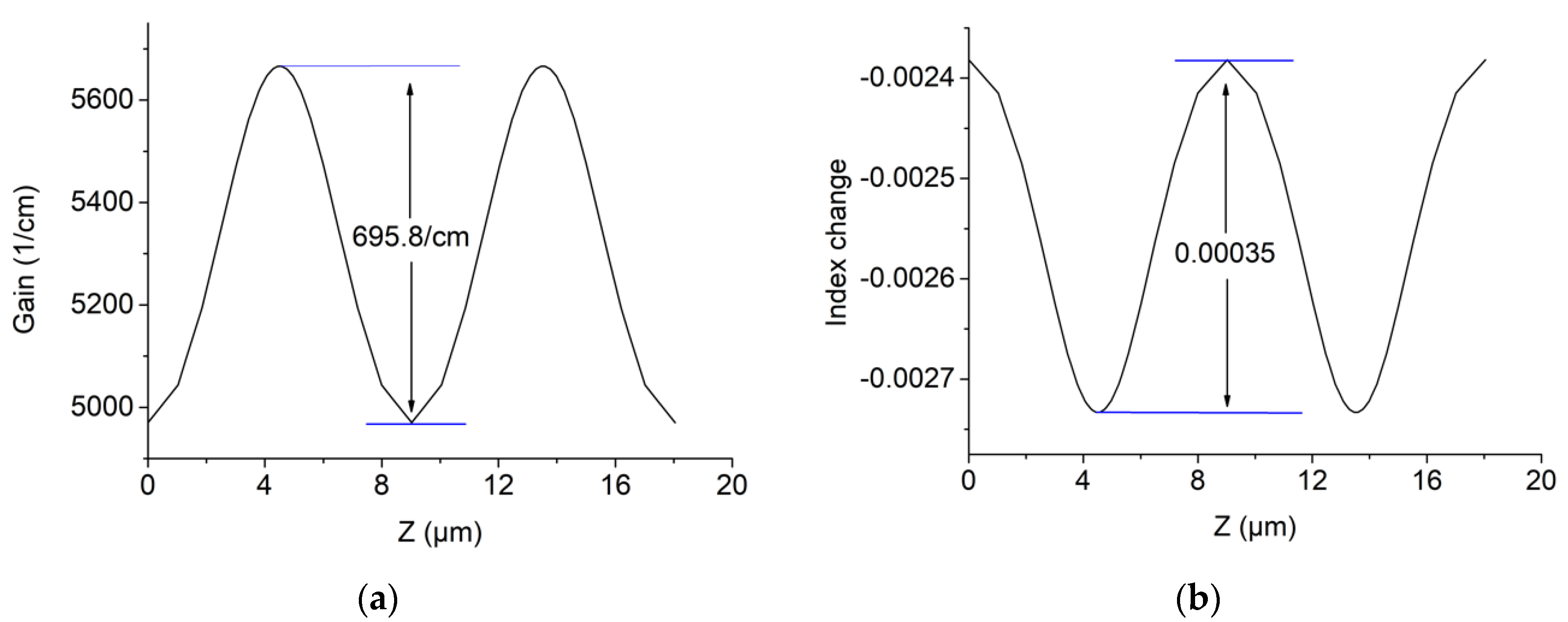
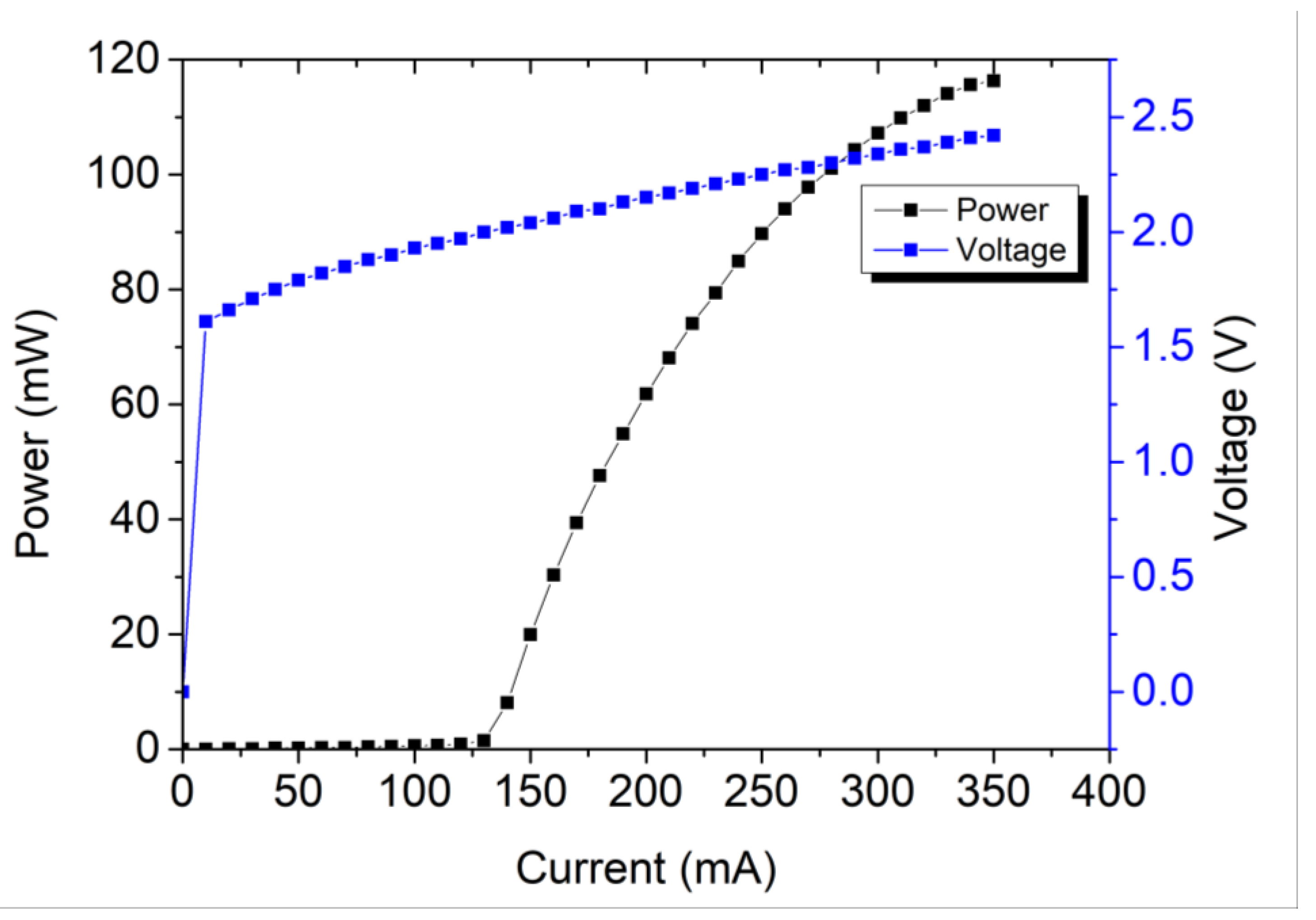
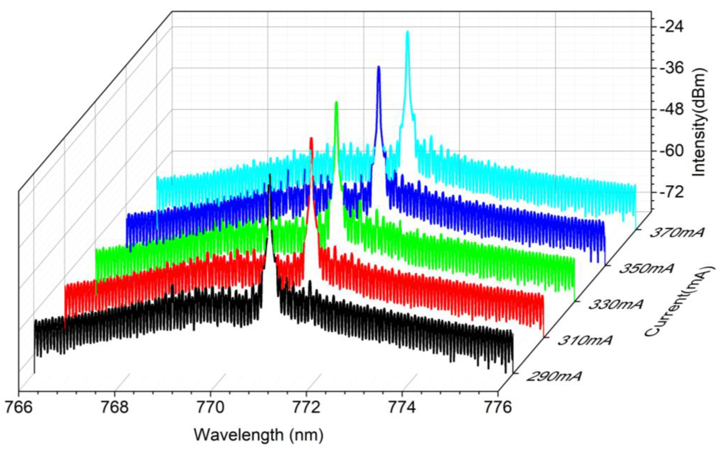
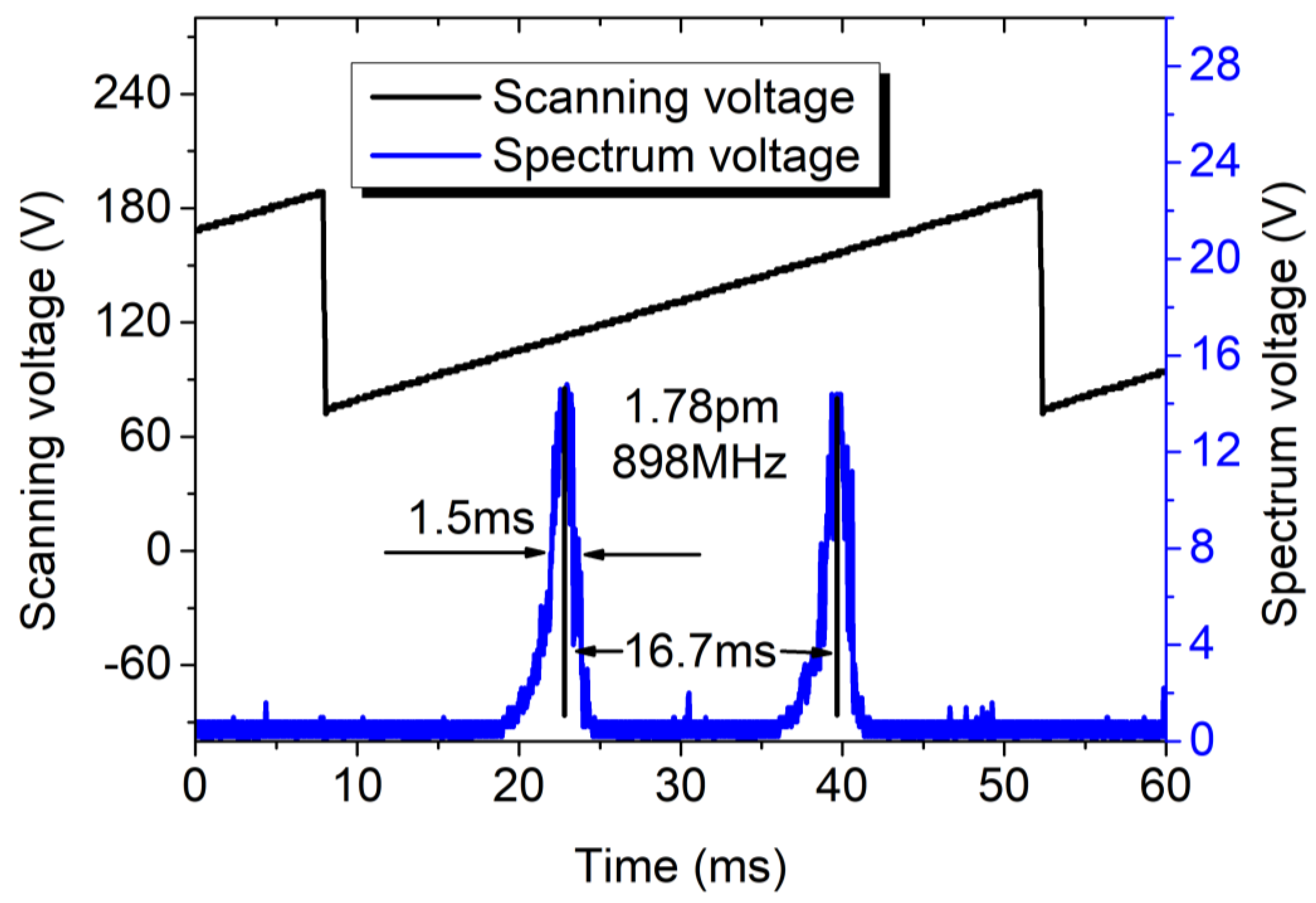
3. Results and Discussion

The power-current-voltage characteristics with continuous-wave (CW) operation at 20 °C are shown in Figure 3. The DFB lasers have a cavity length of 1 mm, with facet coating (high reflection >99%, antireflection <0.5%). The maximum CW power of the devices in single-longitudinal-mode operation is as high as 116.3 mW at 350 mA, which is better than that of the laterally coupled ridge-waveguide (LC-RWG) surface gratings of the DFB lasers (which is 28.9 mW), reported in [37], and better than commercial DBR lasers (which is 80 mW) [31]. An ECDL can get higher output power [37], even more than 700 mW. However, an ECDL uses external optical element to feedback and select the frequency of the laser, which increases the effective length of the resonator. The stability of the coupling optical path and working environment of external optical element is higher. In addition, the external optical frequency selective component coupling optical path and the working environment have high requirements for stability. To realize single longitudinal mode, single chip solutions are always compact and highly integrated as compared with external cavities [32]. Compared with commercially available DBR lasers [31], our device shows the advantage of easy fabrication process with only periodic injection windows, instead of using nanoscale grating fabrication or secondary epitaxy. Different from DBR lasers, our periodically injected current assured our device is working at single longitudinal mode under gain coupled mechanism and with a higher output power of 116.3 mW.
Below the threshold current, the output power of the laser is negligibly small; above the threshold current, when the gain is able to cover the intrinsic and mirror losses, the output power increases almost linearly until saturation, as shown in Figure 3. The power-current curve becomes nonlinear when saturation occurs. There are two main reasons for nonlinearity at saturation as follows: (i) As the current increases, gain saturation appears, and the gap between the peak and the valley of the gain in the laser decreases, weakening the gain-coupling effect. This results in multimode lasing, and the current-power curve no longer conforms to linearity. (ii) When the current increases further, gain saturation generally also appears in the quantum well, and there is no gain contrast. The increase in heat reduces the gain of the quantum well, leading to nonlinearity.
As shown in Figure 4, the wavelength gradually red shifts as the current increases. The single-longitudinal-mode lasing spectrum of our devices in the injection current range of 290–370 mA is pretty well, and the side-mode-suppression ratios (SMSRs) are greater than 30 dB. At 20 °C, the maximum SMSR of our devices is 31.15 dB at 310 mA, and the tuning range of the wavelength vs. current is from 770.91 nm to 771.24 nm in the injection current range 290–370 mA. The mode-hop-free tuning range for the FP mode is 0.052 nm.
As shown in Figure 5a, the SMSR of coated DFB lasers in single-longitudinal-mode operation is as high as 33.25 dB for emission at 770.09 nm (measured with a YOKOGAWA AQ6370C optical spectrum analyzer linked by a single mode fiber with core diameter of 5 μm). Figure 5a shows a typical device spectrum. There are many small peaks along with the main one; the typical interval between these adjacent small peaks is 0.0665 nm. This value closely matches the interval of the FP modes. Figure 5b shows that the wavelength gradually red shifts as the temperature increases. In addition to the gain-coupled effect, the device also has a mode-selection mechanism from the FP cavity. This mechanism has the effect of narrowing the linewidth while causing tuning-wavelength discontinuities, as shown in Figure 5b. Since the gain-coupled effect is relatively weak, it only plays a secondary role in mode selection as compared with the FP modes.
Figure 6 shows the linewidth pattern of the coated DFB laser device measured by coupling the collimating laser into a Fabry–Perot interferometer (Thorlabs, 260SA200-8B). The Fabry–Perot interferometer’s free spectral range is 10 GHz, and the resolution is 67 MHz.
The linewidth Δ v is calculated by
Δ v = v 0 T F W H M / T
where v 0 is free spectral range, T is the interval between the spectral peaks, and TFWHM is the full width at half maximum of the spectrum. As shown in Figure 6, the 3 dB spectral linewidth is 1.78 pm.

4. Conclusions

In this paper, we demonstrated a new type of purely gain-coupled DFB laser based on periodic injection windows working at 770 nm. The periodically injected current maintained the periodic gain of our device and managed to pick out an FP mode to realize single longitudinal mode lasing under gain coupled mechanism in the unetched FP cavity. Our devices have the following excellent characteristics: maximum output power 116.3 mW, maximum SMSR 33.25 dB, and 3 dB linewidth 1.78 pm. Meanwhile, the fabrication process required only general i-line-lithography. No secondary epitaxy or nanoscale grating fabrication technique was needed. In addition, our DFB laser is compact and highly integrated as compared with external cavities and has better output power as compared with commercial pruducts, resulting in a cost-effective way of making DFB lasers to satisfy the booming market of atomic clocks and laser gyroscopes in robots, and thus having great commercial potential.

Author Contributions

Conceptualization, Y.C. and L.Q.; methodology, C.R. and Y.C.; software, Z.Z. and Y.S.; validation, C.R. and Y.C.; formal analysis, C.R., P.J., Z.L., and Y.Z.; investigation, P.J., N.Z., Y.L., and Y.Z.; resources, L.Q. and Y.Z.; data curation, C.R. and Y.C.; writing—original draft preparation, C.R.; writing—review and editing, Y.C.; visualization, C.R.; supervision, Y.C. and L.Q.; project administration, L.Q.; funding acquisition, L.Q. All authors have read and agreed to the published version of the manuscript.

Funding

This research was funded by the National Science and Technology Major Project of China (2017YFB0503100, 2018YFB0504600, 2018YFB2200300); the Frontier Science Key Program of the President of the Chinese Academy of Sciences (QYZDY-SSW-JSC006); the National Natural Science Foundation of China (NSFC) (62090051, 62090052, 62090054, 11874353, 61935009, 61934003, 61904179, 61727822, 61805236,62004194); the Science and Technology Development Project of Jilin Province (20200401069GX, 20200401062GX, 20200501007GX, 20200501008GX, 20200501009GX); the Special Scientific Research Project of Academician Innovation Platform in Hainan Province (YSPTZX202034), and the Dawn Talent Training Program of CIOMP. Independent Innovation Project of State Key Laboratory of Luminescence and Applications (SKL1-Z-2020-02).

Institutional Review Board Statement

Not applicable.

Informed Consent Statement

Not applicable.

Data Availability Statement

Not applicable.

Acknowledgments

The authors thank Yongqiang Ning, Lijun Wang, Hao Wu, Lei Liang, Cheng Qiu, Xing Zhang, Xia Liu, and Dezheng Ma, for helping with this article.

Conflicts of Interest

The authors declare no conflict of interest.

References

  1. Kanskar, M.; Cai, J.; Galstad, C.; He, Y.; Macomber, S.H.; Stiers, E.; Tatavarti-Bharatam, S.R.; Botez, D.; Mawst, J.L. High power conversion efficiency and wavelength-stabilized narrow bandwidth 975nm diode laser pumps. In Proceedings of the SPIE—The International Society for Optical Engineering, Orlando, FL, USA, 12 May 2006. [Google Scholar]
  2. Crump, P.; Schultz, C.M.; Wenzel, H.; Knigge, S.; Brox, O.; Maaßdorf, A.; Bugge, F.; Erbert, G. Reliable Operation of 976nm High Power DFB Broad Area Diode Lasers with over 60% POWER Conversion Efficiency. In Novel In-Plane Semiconductor Lasers X; International Society for Optics and Photonics: Bellingham, WA, USA, 2011. [Google Scholar]
  3. Spiebberger, S.; Schiemangk, M.; Wicht, A.; Wenzel, H.; Brox, O.; Erbert, G. Narrow Linewidth DFB Lasers Emitting Near a Wavelength of 1064 nm. J. Lightwave Technol. 2010, 28, 2611–2616. [Google Scholar] [CrossRef]
  4. Dridi, K.; Benhsaien, A.; Zhang, J.; Hinzer, K.; Hall, T.J. Narrow linewidth two-electrode 1560 nm laterally coupled distributed feedback lasers with third-order surface etched gratings. Opt. Express 2014, 22, 19087–19097. [Google Scholar] [CrossRef]
  5. Li, L.; Tang, S.; Huang, L.; Zhang, T.; Li, S.; Shi, Y.; Chen, X. Experimental demonstration of a low-cost tunable semiconductor DFB laser for access networks. Semicond. Ence Technol. 2014, 29, 095002. [Google Scholar] [CrossRef]
  6. Tilma, B.W.; Mangold, M.; Zaugg, C.A.; Link, S.M.; Waldburger, D.; Klenner, A.; Mayer, A.S.; Gini, E.; Golling, M.; Keller, U. Recent advances in ultrafast semiconductor disk lasers. Light Sci. Appl. 2015, 4, e310. [Google Scholar] [CrossRef] [Green Version]
  7. Zheng, J.; Shi, Y.; Zhang, Y.; Zheng, J.; Lu, J.; Chen, X. Monolithically Integrated Four-Channel DFB Semiconductor Laser Array With an Equivalent-Distributed Coupling Coefficient. IEEE Photonics J. 2015, 7, 1. [Google Scholar] [CrossRef]
  8. Nehrir, R.; Repasky, K.S.; Carlsten, J.L. Eye-safe diode-laser-based micropulse differential absorption lidar (DIAL) for water vapor profiling in the lower troposphere. J. Atmos. Ocean. Technol. 2011, 28, 131–147. [Google Scholar] [CrossRef]
  9. Kowalczyk, M.; Sotor, J.; Abramski, K.M. 59 fs mode-locked Yb:KGW oscillator pumped by a single-mode laser diode. Laser Phys. Lett. 2016, 13, 035801. [Google Scholar] [CrossRef] [Green Version]
  10. Noda, C.Q.; Uitenbroek, H.; Katsukawa, Y.; Shimizu, T.; Oba, T.; Carlsson, M.; Suárez, D.O.; Cobo, B.R.; Kubo, M.; Anan, T.; et al. Solar polarimetry through the KI lines at 770 nm. Mon. Not. R. Astron. Soc. 2018, 470, 1453–1461. [Google Scholar] [CrossRef] [Green Version]
  11. Brookes, J.R.; Isaak, G.R.; Van der Raay, H.B. A resonant-scattering solar spectrometer. Mon. Not. R. Astron. Soc. 1978, 185, 1–18. [Google Scholar] [CrossRef] [Green Version]
  12. Bruls, J.H.M.J.; Rutten, R.J. The formation of helioseismology lines. II—Modeling of alkali resonance lines with granulation. Astron. Astrophys. 1992, 265, 257–267. [Google Scholar]
  13. Brox, O.; Bugge, F.; Mogilatenko, A.; Luvsandamdin, E.; Wicht, A.; Wenzel, H.; Erbert, G. Distributed feedback lasers in the 760 to 810 nm range and epitaxial grating design. Semicond. Sci. Technol. 2014, 29, 095018. [Google Scholar]
  14. Serkland, D.K.; Geib, K.M.; Peake, G.M.; Lutwak, R.; Rashed, A.; Varghese, M.; Tepolt, G.; Prouty, M. VCSELs for atomic sensors. In Proceedings of the SPIE—The International Society for Optical Engineering, San Jose, CA, USA, 23 February 2007. [Google Scholar]
  15. Nakano, Y.; Luo, Y.; Tada, K. AlGaAs/GaAs visible distributed feedback laser operating at 770 nm. Electron. Lett. 1987, 23, 1342–1343. [Google Scholar] [CrossRef]
  16. Krysa, A.B.; Roberts, J.S.; Devenson, J.; Beanland, R.; Karomi, I.; Shutts, S.; Smowton, P.M. InAsP/AlGaInP/GaAs QD laser operating at ~770 nm. In Proceedings of the International Symposium on Coherent Optical Radiation of Semiconductor Compounds and Structures, Moscow, Russia, 23–26 November 2016. [Google Scholar]
  17. Reinhold, A.; Fischer, M.; Zeller, W.; Koeth, J.; Höfling, S.; Kamp, M. Evanescently Coupled DBR Laser Arrays in the 760–770 nm Wavelength Range. IEEE Photonics Technol. Lett. 2019, 31, 1319–1322. [Google Scholar] [CrossRef] [Green Version]
  18. Nechay, K.; Kahle, H.; Penttinen, J.P.; Rajala, P.; Tukiainen, A.; Ranta, S.; Guina, M. AlGaAs/AlGaInP VECSELs With Direct Emission at 740–770 nm. IEEE Photonics Technol. Lett. 2019, 31, 1245–1248. [Google Scholar] [CrossRef]
  19. Kogelnik, H.; Shank, C.V. Coupled-wave theory of distributed feedback lasers. J. Appl. Phys. 1972, 43, 2327–2335. [Google Scholar] [CrossRef]
  20. Zuo, Q.; Zhao, J.Y.; Chen, X.; Wang, Z.H.; Sun, T.Y.; Zhou, N.; Zhao, Y.-L.; Xu, Z.-M.; Liu, W. A Multiple Phase-Shifted Distributed Feedback (DFB) Laser Fabricated by Nanoimprint Lithography. Chin. Phys. Lett. 2013, 30. [Google Scholar] [CrossRef]
  21. Zhang, L.M.; Carroll, J.E. Dynamics of index coupled DFB lasers with minimal spatial hole burning. IEEE Photonics Technol. Lett. 2002, 6, 486–488. [Google Scholar] [CrossRef]
  22. Correc, P. Stability of phase-shifted DFB lasers against hole burning. IEEE J. Quantum Electron. 2002, 30, 2467–2476. [Google Scholar] [CrossRef]
  23. Ogita, S.; Kotaki, Y.; Matsuda, M.; Kuwahara, Y.; Ishikawa, H. Long cavity multiple-phase-shift distributed feedback laser for linewidth narrowing. Electron. Lett. 1989, 25, 629–630. [Google Scholar] [CrossRef]
  24. Okai, M.; Tsuchiya, T.; Uomi, K.; Chinone, N.; Harada, T. Corrugation-pitch modulated MQW-DFB lasers with narrow spectral linewidth. IEEE Photonics Technol. Lett. 1991, 27, 1767–1772. [Google Scholar] [CrossRef]
  25. Shi, Y.; Li, S.; Li, J.; Jia, L.; Liu, S.; Chen, X. An apodized DFB semiconductor laser realized by varying duty cycle of sampling Bragg grating and reconstruction-equivalent-chirp technology. Optics Commun. 2010, 283, 1840–1844. [Google Scholar] [CrossRef]
  26. Li, G.P.; Makino, T. Single-mode yield analysis of partly gain-coupled multiquantum-well DFB lasers. IEEE Photonics Technol. Lett. 1993, 5, 1282–1284. [Google Scholar] [CrossRef]
  27. Nakano, Y.; Luo, Y.; Tada, K. Facet reflection independent, single longitudinal mode oscillation in a GaAlAs/GaAs distributed feedback laser equipped with a gain-coupling mechanism. Appl. Phys. Lett. 1989, 55, 1606–1608. [Google Scholar] [CrossRef]
  28. Luo, Y.; Nakano, Y.; Tada, K.; Inoue, T.; Hosomatsu, H.; Iwaoka, H. Purely gain-coupled distributed feedback semiconductor lasers. Appl. Phys. Lett. 1990, 56, 1620–1622. [Google Scholar] [CrossRef]
  29. Chen, Y.; Jia, P.; Zhang, J.; Qin, L.; Chen, H.; Gao, F.; Zhang, X.; Shan, X.; Ning, Y.; Wang, L. Gain-coupled distributed feedback laser based on periodic surface anode canals. Appl. Opt. 2015, 54, 8863. [Google Scholar] [CrossRef] [PubMed]
  30. Gao, F.; Qin, L.; Chen, Y.; Jia, P.; Chen, C.; Cheng, L.; Chen, H.; Liang, L.; Zeng, Y.; Zhang, X.; et al. Study of gain-coupled distributed feedback laser based on high order surface gain-coupled gratings. Opt. Commun. 2018, 410, 936–940. [Google Scholar] [CrossRef]
  31. Available online: http://www.photodigm.com/products/770-nm-laser-diode (accessed on 20 January 2021).
  32. Stry, S.; Thelen, S.; Sacher, J.; Halmer, D.; Hering, P.; Mürtz, M. Widely tunable diffraction limited 1000 mW external cavity diode laser in Littman/Metcalf configuration for cavity ring-down spectroscopy. Appl. Phys. B 2006, 85, 365–374. [Google Scholar] [CrossRef]
  33. Ito, F.; Tanifuji, T. Carrier-injection-type optical switch in GaAs with a 1.06–1.55 μm wavelength range. Appl. Phys. Lett. 1989, 54, 134–136. [Google Scholar] [CrossRef]
  34. Wang, B. Reseach on All Optical Solid-state X-ray Detection with Picosecond Resolusion Based on Refractive Index Modulation. Ph.D. Thesis, University of Chinese Academy of Sciences, Bejing, China, 2016. [Google Scholar]
  35. David, K.; Morthier, G. Gain-coupled DFB lasers versus index-coupled and phase-shifted DFB lasers: A comparison based on spatial hole burning corrected yield. IEEE J. Quantum Electron. 1991, 27, 1714–1723. [Google Scholar] [CrossRef]
  36. Decker, J.; Crump, P.; Fricke, J.; Maassdorf, A.; Erbert, G.; Trankle, G. Narrow Stripe Broad Area Lasers With High Order Distributed Feedback Surface Gratings. IEEE Photonics Technol. Lett. 2014, 26, 829–832. [Google Scholar] [CrossRef]
  37. Virtanen, H.; Uusitalo, T.; Karjalainen, M.; Ranta, S.; Viheriälä, J.; Dumitrescu, M. Narrow-Linewidth 780-nm DFB Lasers Fabricated Using Nanoimprint Lithography. IEEE Photonics Technol. Lett. 2017, 30, 51–54. [Google Scholar] [CrossRef]
Figure 1. (a) Schematic of the epitaxial structure of our device; (b) Scanning electron microscope image of a device; (c) Transverse-mode distribution map simulated by COMSOL Multiphysics; (d) Schematic of carrier-distribution cross section for periodic electric injection.
Applsci 11 01531 g001
Figure 2. (a) One-dimensional gain distribution in the quantum well; (b) One-dimensional index change in the quantum well.
Applsci 11 01531 g002
Figure 3. Power-current-voltage curve of the devices at 20 °C.
Applsci 11 01531 g003
Figure 4. Typical device spectrum as a function of current at 20 °C.
Applsci 11 01531 g004
Figure 5. (a) Typical device spectrum at 300 mA at 11 °C; (b) Effect of temperature on the spectrum at 300 mA.
Applsci 11 01531 g005
Figure 6. Linewidth pattern of the devices.
Applsci 11 01531 g006
Table 1. Properties of the epitaxial wafer.
MaterialStructureThickness (μm)Dopant
GaAsCap0.1Carbon
Al(x)GaAsP-cladding0.8Carbon
Al(x)GaAsP-wave guide0.4Carbon
Al(x)In(y)GaAsQuantum well0.0055Undoped
Al(x)GaAsN-wave guide1Silicon
Al(x)GaAsN-cladding1.5Silicon
GaAsBuffer0.5Silicon
Publisher’s Note: MDPI stays neutral with regard to jurisdictional claims in published maps and institutional affiliations.

