Review

Development of an Epitaxial Growth Technique Using III-V on a Si Platform for Heterogeneous Integration of Membrane Photonic Devices on Si

1
NTT Device Technology Labs, NTT Corporation, 3-1 Morinosato-Wakamiya, Atsugi-shi, Kanagawa 243-0198, Japan
2
Currently with the Graduate School of Information, Production and Systems, Waseda University, 2-7 Hibikino, Wakamatsu-ku, Kitakyushu-shi, Fukuoka 808-0135, Japan
*
Author to whom correspondence should be addressed.
Appl. Sci. 2021, 11(4), 1801; https://doi.org/10.3390/app11041801
Submission received: 28 December 2020 / Revised: 12 February 2021 / Accepted: 12 February 2021 / Published: 18 February 2021

Abstract

:

Featured Application

Optical interconnects for data centers.

Abstract

The rapid increase in total transmission capacity within and between data centers requires the construction of low-cost, high-capacity optical transmitters. Since a tremendous number of transmitters are required, photonic integrated circuits (PICs) using Si photonics technology enabling the integration of various functional devices on a single chip is a promising solution. A limitation of a Si-based PIC is the lack of an efficient light source due to the indirect bandgap of Si; therefore, hybrid integration technology of III-V semiconductor lasers on Si is desirable. The major challenges are that heterogeneous integration of III-V materials on Si induces the formation of dislocation at high process temperature; thus, the epitaxial regrowth process is difficult to apply. This paper reviews the evaluations conducted on our epitaxial growth technique using a directly bonded III-V membrane layer on a Si substrate. This technique enables epitaxial growth without the fundamental difficulties associated with lattice mismatch or anti-phase boundaries. In addition, crystal degradation correlating with the difference in thermal expansion is eliminated by keeping the total III-V layer thickness thinner than ~350 nm. As a result, various III-V photonic-device-fabrication technologies, such as buried regrowth, butt-joint regrowth, and selective area growth, can be applicable on the Si-photonics platform. We demonstrated the growth of indium-gallium-aluminum arsenide (InGaAlAs) multi-quantum wells (MQWs) and fabrication of lasers that exhibit >25 Gbit/s direct modulation with low energy cost. In addition, selective-area growth that enables the full O-band bandgap control of the MQW layer over the 150-nm range was demonstrated. We also fabricated indium-gallium-arsenide phosphide (InGaAsP) based phase modulators integrated with a distributed feedback laser. Therefore, the directly bonded III-V-on-Si substrate platform paves the way to manufacturing hybrid PICs for future data-center networks.

1. Introduction

Increased data transmission between and within data centers requires high-capacity and low-cost optical links. To meet the requirement for a tremendous number of photonic components for such short-distance applications, the integration of various photonic devices into a single chip becomes key because the assembly process can be dramatically simplified. Therefore, photonic integrated circuits (PICs) using Si photonics technology are promising because mature complementary-metal-oxide-semiconductor (CMOS) fabrication technology enables the integration of various optical devices into a compact chip [1,2,3,4,5,6,7,8,9,10]. A limitation of a Si-photonics-based PIC is the lack of a reliable, efficient and low-power-consumption light source due to its indirect bandgap. Accordingly, the integration of direct-bandgap III-V semiconductors on Si is desirable. In particular, indium phosphide (InP) and its related materials are widely used for developing high-performance optical transmitters such as directly modulated lasers (DMLs), electro-absorption modulator-integrated distributed feedback (EADFB) lasers and Mach-Zehnder modulators (MZMs) [11,12,13,14,15,16,17,18]. Therefore, several hybrid integration techniques are used to develop III-V/Si hybrid PICs [4,19,20,21,22].
Among the hybrid integration techniques, direct epitaxial growth of III-V materials on a Si substrate has been attracting much attention for over 30 years because it is the most promising technique in terms of cost and scalability. However, there are fundamental difficulties that limit crystal quality such as differences in lattice constant, differences in the coefficient of thermal expansion (CTE), and the formation of anti-phase boundaries (APBs). In 1990, Sugo et al. demonstrated the room-temperature (RT) operation of indium-gallium-arsenide phosphide (InGaAsP) lasers directly grown on a Si substrate [23]. However, a buffer layer thicker than 15 μm was required, making them difficult to optically connect to Si-photonics devices. Much effort has been made to improve the crystal quality of multi-quantum wells (MQWs) with thinner buffer layers [24,25]. In addition, III-V quantum dot (QD) lasers directly grown on a Si substrate that exhibit >100 mW optical output power have been demonstrated [26,27]. This can be achieved because QDs are insensitive to threading dislocations (TDs) compared with QWs. However, these “blanket” epitaxial growth techniques still require a thick buffer layer (typically >2 μm). In contrast, direct selective epitaxy using defect filtering with selective-area growth masks enable the integration of high-quality III-V layers on a Si substrate without requiring a thick buffer layer [28,29,30,31,32]. Using the defect filtering method, various lasers with optical pumping have been demonstrated. On the other hand, electrically driven lasers that can emit output power required for data-center application have yet to be reported. This seems to correlate with the difficulty of growing ternary and quaternary compound materials, such as indium-gallium arsenide (InGaAs), InGaAsP, and indium-gallium-aluminum arsenide (InGaAlAs), because the crystal composition of these materials depends on both the mask structure and distance from the mask edge [33]. In addition, the structural limitation of the III-V device layer due to the selective-area growth masks makes it difficult to fabricate a p-i-n junction, which is necessary for current injection.
Direct- and adhesive-bonding techniques are another possible solution to achieve wafer-scale heterogeneous integration because bonding prevents the formation of TDs and APBs in III-V layers [34,35]. By using direct bonding of III-V active layers, III-V/Si hybrid lasers that have III-V active regions optically connected to Si waveguides have been demonstrated [36,37,38]. In addition, micro-transfer-printing has attracted attention as a promising means to integrate III-V optical devices on Si-photonics components [19,39,40,41]. This is because it enables the manipulation of micron-size III-V layer coupons on a donor III-V substrate, and the substrate can be used repeatedly. With these bonding techniques, III-V/Si hybrid PICs have been demonstrated and the directly bonded III-V lasers exhibit sufficient optical output power as a continuous wave light source for Si-photonics modulators. As transmitters for data-center application, however, the footprint and power consumption of DMLs on a Si substrate should be further improved. This is due to a lack of epitaxial regrowth in III-V/Si bonding; an InGaAlAs/InP or InGaAsP/InP buried-heterostructure (BH) fabricated by epitaxial regrowth of InP is essential for reliable, low-power-consumption DMLs because a BH enables high optical- and carrier-confinement into the active region [42,43].
Consequently, direct bonding of III-V membrane layers on a Si substrate followed by epitaxial regrowth of InP-based material is an effective technique [44,45,46,47,48,49,50,51,52]. This technique overcomes the problems with direct epitaxial growth and bonding techniques. In terms of epitaxial growth, a III-V membrane layer on Si as an epitaxial template prevents lattice mismatching and APBs. Regarding device fabrication, the capability of epitaxial growth on Si offers high flexibility of the III-V device design. In particular, it enables the integration of different III-V mediums on the same plane such as BHs, butt-joint (BJ) structures [15,53], and multi-wavelength gain structures. However, most studies suffered from the strain induced by the mismatch of the CTE, and threading dislocation densities (TDDs) of epitaxial layers are not as low as those of a standard InP substrate (<1 × 10⁴/cm2). This is because the thickness of the total III-V layer after regrowth is thicker than the critical thickness, which is determined by the product of temperature change and mismatch of CTE between Si and InP. It is calculated to be ~430 nm when we assume the bonding temperature and epitaxial growth temperature are 200 and 600 °C, respectively [46,54], which is much thinner than the total thickness of typical InP-based lasers with vertical p-i-n structure for electrical pumping.
In this context, we developed an epitaxial growth technique that uses an InP membrane layer formed on a Si substrate for lateral p-n or p-i-n membrane structure. Since we keep the total III-V thickness less than the critical thickness determined by the thermal strain throughout the process, a superior-quality III-V epitaxial layer that has a TDD as low as the standard InP substrate can be achieved. In this paper, we discuss the evaluations on epitaxial growth technique and lasers fabricated using a III-V membrane on a Si-based substrate. Section 2 first describes our integration procedure to obtain high-quality III-V membrane photonic devices on a Si substrate. After discussing the critical thickness of the III-V membrane on a Si substrate at the epitaxial growth temperature, the crystal quality of epitaxial grown InP and InGaAlAs is evaluated in detail. Section 3 provides the detailed characteristics of membrane lasers, including an InGaAlAs DML array on Si fabricated using epitaxial grown MQWs on an InP-on-insulator substrate. In addition, recent efforts to integrate multi-bandgap III-V photonic devices using epitaxial growth on the Si-photonics platform, such as a wide-wavelength-range laser array and InGaAsP-MZM integrated with a DFB laser, are reported.

2. Epitaxial Growth on InP-on-Insulator Substrate

For III-V/Si hybrid integration, the crystal quality of the III-V layer after heterogeneous integration is important. To achieve high crystal quality, several low-temperature bonding techniques that enable stable and strong bonding at annealing temperatures below 400 °C were developed. Compared to conventional high-temperature fusion bonding, they enable significant improvements in crystal quality of the III-V layer, resulting in high-performance hybrid PICs. On the other hand, to avoid thermal degradation, process temperatures higher than 400 °C are still prohibitive after bonding, meaning that the epitaxial regrowth of III-V material cannot be carried out on a Si substrate.
High-quality epitaxial growth has recently become possible by limiting the total III-V layer thickness. We focus on how epitaxial growth on a III-V-on-insulator substrate is achieved.

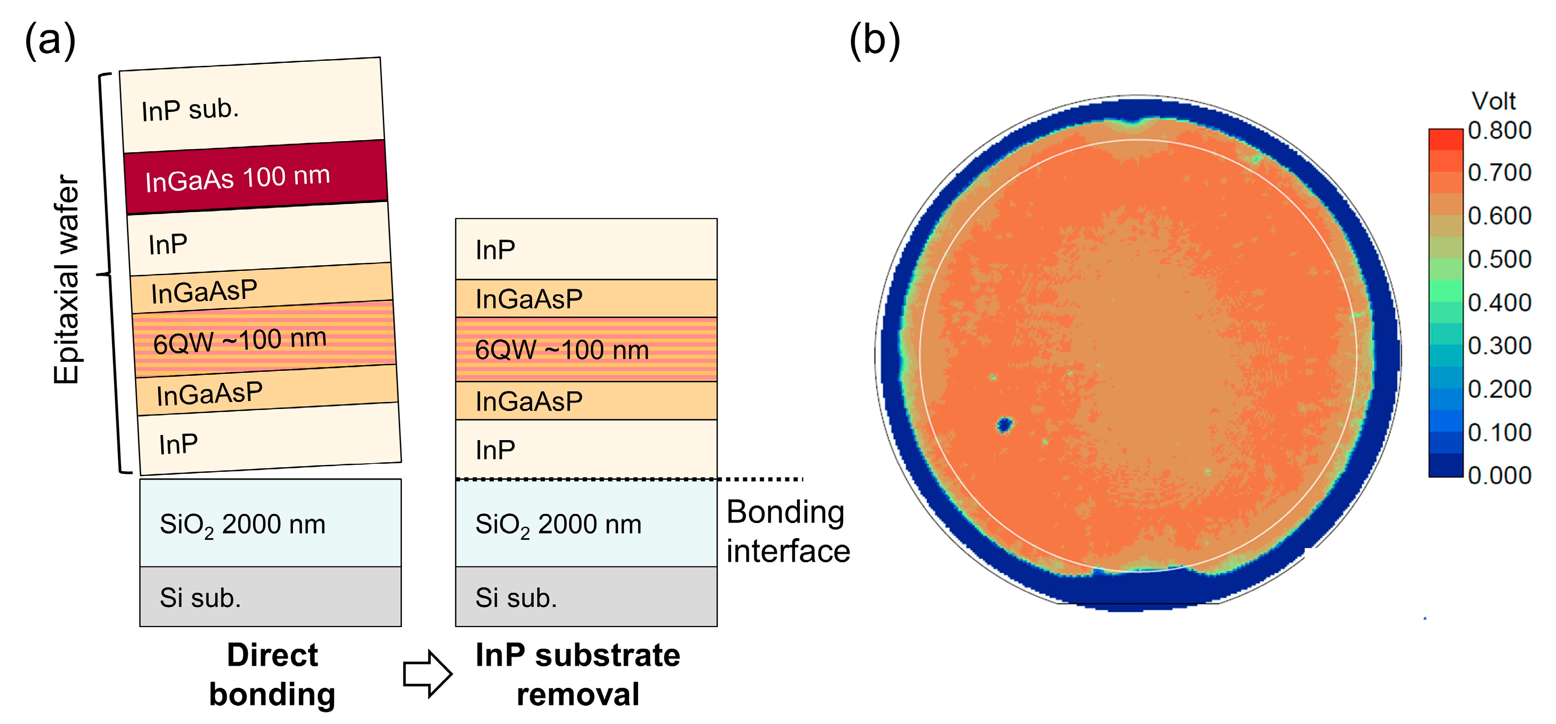
2.1. Integration Method of III-V Photonic Devices on Si

Figure 1 shows the process flow of fabricating membrane photonic devices on Si using epitaxial growth technique on III-V-on-insulator platform. The process begins with the epitaxial growth of a III-V epitaxial layer including InP membrane layer and InGaAs etch-stop layer on standard InP substrate. Next, the epitaxial InP wafer and a Si wafer are bonded. Then, the InP membrane layer is left on the SiO2 layer by removing the InP substrate and InGaAs etch-stop layer (InP-on-insulator substrate). After that, a III-V active layer such as InGaAsP/InGaAsP- or InGaAlAs/InGaAlAs-MQW double-heterostructure (DH) sandwiched between the InP layer is grown on InP-on-insulator substrate as an active region for photonic devices. The MQW-DH is then etched by dry- and selective wet-etching, which leaves an InP layer except for under the SiO2 mask (mesa-stripe). After that, undoped InP is selectively grown on the InP membrane to fabricate the BH, which enables high optical- and carrier-confinement into the active region. Finally, formation of the lateral p-i-n or p-n junction and metallization are carried out to fabricate the membrane photonic devices.

2.2. Assessment of Thermal Strain at Epitaxial Growth Temperature

To grow a high-quality epitaxial layer using a III-V/Si integrated substrate, the total III-V layer thickness is critical [46]. This subsection describes the calculation model of the critical thickness of the InP layer on an InP-on-insulator substrate. Since the process temperature of metalorganic vapor phase epitaxy (MOVPE) for InP-based materials is about 600 °C, the difference of the CTEs between InP-based materials and SiO2/Si causes thermal strain. Thermal strain ε is given by the product of the difference between the CTEs ∆α and temperature change ∆T. The CTEs of Si and InP at 25 °C are 2.62 and 4.56 ppm/K, respectively [55]. For simplification, we disregard the SiO2 layer because it is much thinner (typically 2 μm) than the Si substrate. Since we apply pressure to the bonded wafer at 200 °C, we assume that the directly bonded InP membrane layer is free standing at 200 °C. On the basis of the above, epitaxial growth temperature (600 °C) induces a compressive strain of approximately 780 ppm to the InP membrane layer on Si.
Next, the critical thickness was calculated based on the thermal strain applied at epitaxial growth temperature. When the total InP-based layer is thicker than the critical thickness, a dislocation should be generated in both the original InP membrane and regrown layer, resulting in degradation of photoluminescence (PL) and electroluminescence characteristics. There are two types of models to calculate critical thickness, mechanical equilibrium models and strain–energy–density equilibrium models. The thickness at which the dislocations appear in the actual strained crystal tends to be between the critical thicknesses calculated using these models [56].
Figure 2 compares the critical thickness versus strain calculated using one of each type of calculation model. The mechanical equilibrium model expresses the critical thickness hc as follows [57]:
h c = b ( 1 ν / 4 ) 4 π f ( 1 + ν ) ( ln h c b + 1 ) ,
where ν is Poisson′s ratio for strained material, b is Burger′s vector of dislocation, and f is strain. On the other hand, the strain–energy–density equilibrium model expresses the critical thickness as follows [54]:
h c = 6 b ( 2 ν ) 8 3 / 2 π f ( 1 + ν ) { ln ( 8 3 / 2 a h c b ) 2 } ,
where a is a parameter that is related to the dislocation energy (typically a ~ 4). On the basis of the two models, the critical thickness of InP on a SiO2/Si substrate is calculated to be between approximately 200 nm (mechanical equilibrium model) and 430 nm (energy equilibrium model) for a thermal strain of about 800 ppm. Therefore, high-temperature MOVPE growth should not induce the formation of dislocation even though the III-V/Si hybrid substrate is used, unless the InP membrane thickness after the growth exceeds 200 or 430 nm.
To experimentally evaluate the critical thickness, we fabricated III-V membranes that are bonded to SiO2/Si substrates [46]. Figure 3a shows the process flow. The fabrication began with the epitaxial growth of an InP buffer layer, InGaAs etch-stop layer (100 nm), and MQW double-heterostructure (DH) sandwiched between the InP layer on a 2-inch standard InP (001) substrate by MOVPE. The growth was undertaken at 630 °C and 6.7 kPa, and the precursors for In, Ga, As and P were trimethyl-indium (TMI), triethyl-gallium (TEG), arsine (AsH3) and phosphine (PH3), respectively. The DH included six-period strained InGaAsP MQWs (PL peak wavelength: 1520 nm). The epitaxial InP wafer and a 2-inch Si (001) wafer with a 2-μm-thick thermal silicon dioxide (SiO2) layer (SiO2/Si substrate) were treated with oxygen plasma. This process grew the ultra-thin oxide layer, which makes the bonding surface very smooth and hydrophilic [58]. The wafers were then directly bonded at RT under atmospheric pressure. After that, post-annealing was carried out at 200 °C while pressure from 1.0 to 6.1 MPa was applied. To leave the InP-based membrane layers on the SiO2 layer, the InP substrate side was mechanically polished and chemically etched using the InGaAs etch-stop layer [59]. Finally, the InGaAs etch-stop layer was chemically etched to obtain a 250-nm-thick MQW-DH on the SiO2 layer. Figure 3b shows a typical PL intensity maps for the 250-nm-thick MQW-DH on the SiO2/Si substrate at 25 °C, measured with the excitation laser irradiation at a wavelength of 980 nm. The PL intensity distribution was very uniform (standard deviation: 1.31%), excluding the peeled region at the wafer edge.
Next, we prepared three MQW-DHs on SiO2/Si substrate with various III-V layer thicknesses and characterized their PL before and after 610 °C annealing (epitaxial regrowth temperature). The three epitaxial wafers included almost the same MQWs, but the total III-V layer thicknesses were varied from 250 to 850 nm. We annealed these wafers in an MOVPE reactor for 30 min under the PH3-atmosphere epitaxial-regrowth condition. The temperature was 610 °C and the pressure was 4.0 kPa. Figure 4a–c compares the PL spectra before (solid lines) and after (dashed lines) the MOVPE annealing for the samples with three different thicknesses, respectively. The median PL intensity for the wafer with a total thickness of 250 nm degraded only 8% after annealing. In contrast, for samples with total thicknesses of 500 and 850 nm which are thicker than the critical thicknesses calculated with the two models, degradation increased to 31 and 68%, respectively. To evaluate the degradation in the epitaxial wafers, we also evaluated the PL-intensity map with a PL microscope that can visualize dislocations and clacks. Figure 4d–f compares the PL-intensity distributions measured with PL microscope for these three samples. They clearly show that there were neither dark line nor dark spots in the 100 × 100 μm2 area for the 250-nm-thick sample, whereas dark lines were observed for the 500- and 850-nm-thick samples [46]. We also confirmed that a dark line did not appear when the total III-V thickness was 350 nm [60]. These results clearly show that the actual critical thickness for an InP-based membrane layer on a Si substrate at 610 °C should be between 350 and 500 nm; therefore, epitaxial regrowth using an InP-on-insulator substrate should not induce dislocation when the total III-V thickness is less than 350 nm.

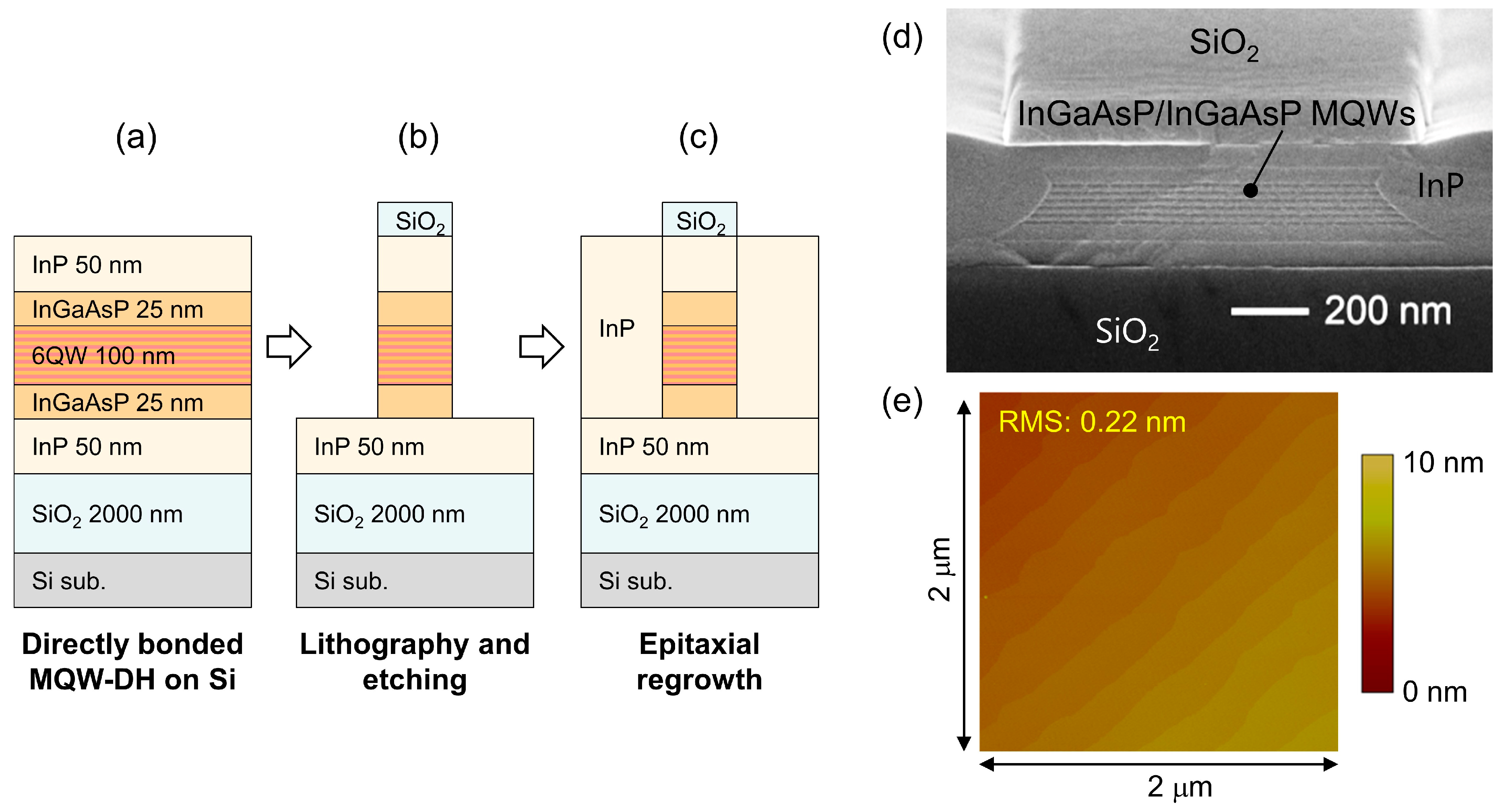
2.3. Regrowth of InP

The epitaxial regrowth of InP on an InP-on-insulator substrate is an important process because it enables the fabrication of a BH on a SiO2/Si substrate, which makes it possible to integrate low-power-consumption-membrane optical devices on a Si substrate. Figure 5a–c shows the process flow of fabricating a BH. First, an MQW-DH was grown on standard InP substrate and transferred to thermally oxidized Si substrate by using a direct bonding technique. Next, a SiO2 layer was deposited using plasma-enhanced chemical vapor deposition (p-CVD). An ~800-nm-wide SiO2 mask was formed using lithography and reactive ion etching (RIE). The MQW-DH was then etched by dry- and selective wet-etching, which leaves a 50-nm-thick InP layer except for under the SiO2 mask (mesa-stripe) [59,61,62]. After that, undoped InP was grown on the InP membrane, except for the SiO2 mask, to fabricate the InGaAsP/InP BH. The epitaxial growth temperature was 610 °C and the pressure was 4.0 kPa. The growth rate was ~0.4 μm/h. Figure 5d shows a cross-sectional scanning electron microscope (SEM) image of a BH on the SiO2/Si substrate. The 150-nm-thick and 800-nm-wide active region was successfully buried in InP. Figure 5e shows an atomic force microscope (AFM) image of the surface of a regrown InP layer on a SiO2/Si substrate. Clear atomic steps were observed, and the root-mean-square roughness was 0.22 nm, which are comparable to the surface morphology of a standard InP epitaxial layer on an InP substrate.

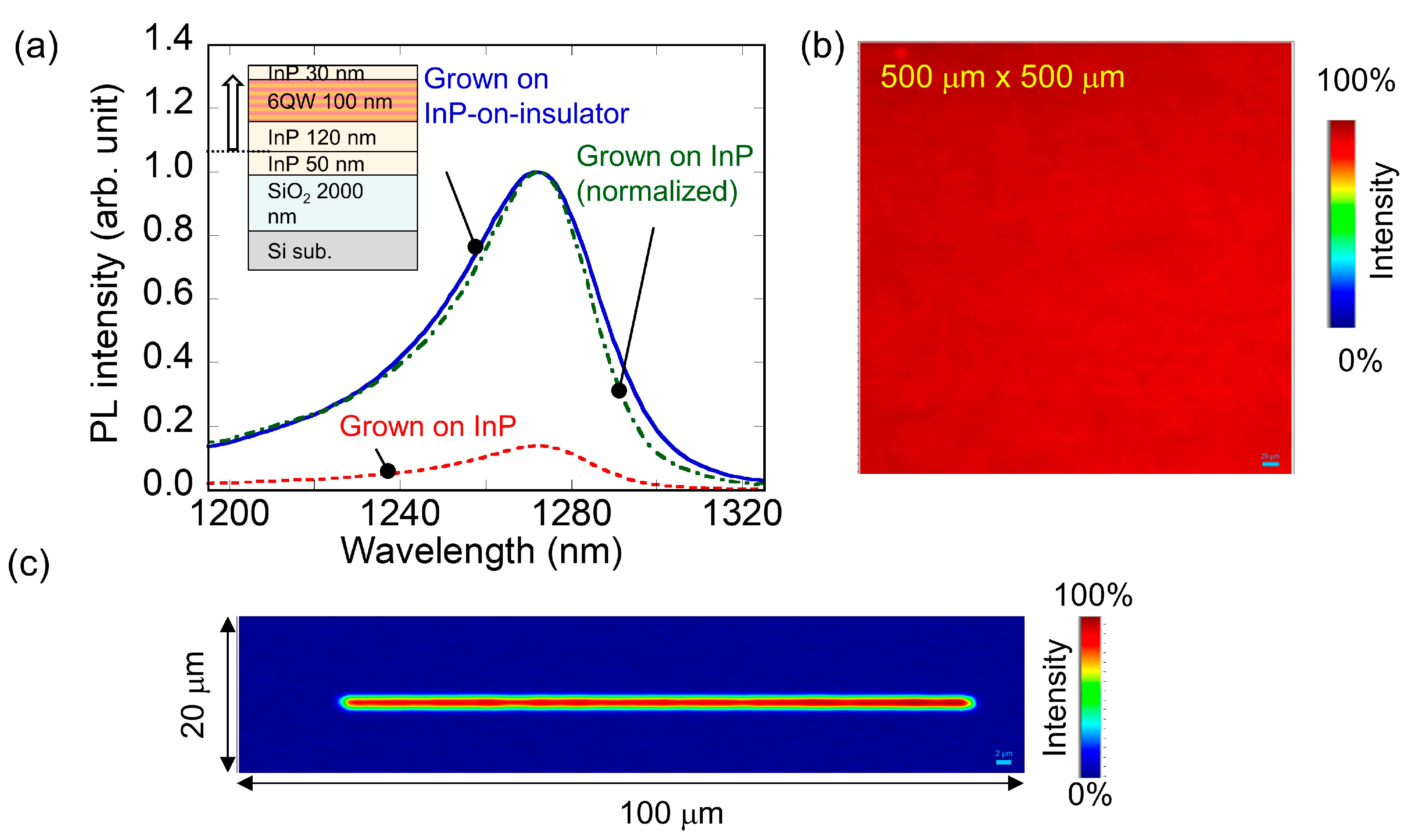
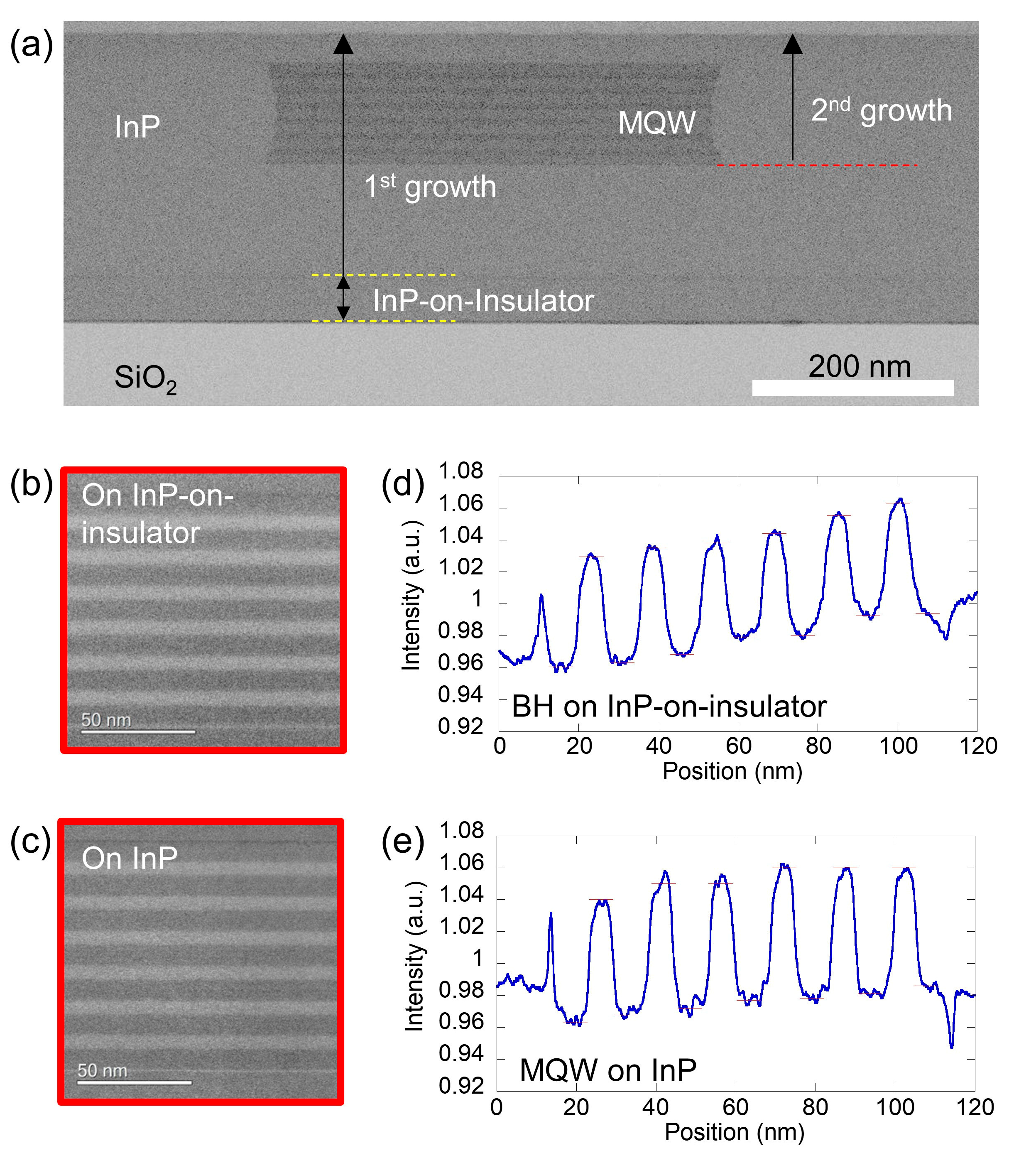
2.4. Growth of Multi-Quantum-Well Double-Hetero Structure

To integrate III-V photonic devices with different bandgap active regions on a Si substrate, the growth of a ternary or quaternary compound semiconductor is also necessary. In particular, a strained MQW is widely used as an active region for state-of-the-art DMLs and electro-absorption modulators [63,64,65,66]. We demonstrated the growth of MQWs on InP-on-insulator followed by epitaxial regrowth of InP to fabricate a BH, by keeping the total thickness to less than 350 nm. We prepared an InP-on-insulator substrate that includes 50-nm-thick InP membrane layer by direct bonding. Then, a 120-nm-thick InP buffer layer, 6-period MQW, and 30-nm-thick InP cap layer were grown on it. Both InGaAsP/InGaAsP and InGaAlAs/InGaAlAs have been demonstrated as MQW material [47,67,68]. The growth temperature was estimated to be around 630 °C, and the pressure was about 6.7 kPa under hydrogen carrier gas. The precursors for In, Ga, Al, As, and P were TMI, TEG, trimethyl-aluminum, AsH3, and PH3, respectively. The epitaxial layer quality was characterized by PL measurements. Figure 6a compares the PL spectra of an InGaAlAs MQW grown on an InP-on-insulator substrate and the same MQW grown on a standard InP substrate as a reference. To achieve high crystal quality, we controlled the residual strain in the MQW on InP-on-insulator substrate to be -680 ppm (tensile), which almost cancels the compressive thermal strain induced at the growth temperature [47,69]. The peak PL intensity of the MQW grown on the InP-on-insulator substrate was 7.2 times greater than that of the reference grown on the InP substrate because both the excitation and collection efficiency of PL were enhanced due to the underlying InP/SiO2/Si interfaces [46,51]. The slightly broadened full width at half maximum of the PL (30.0 to 33.4 meV) seems to be because of the higher excitation energy density, and there were no significant differences for spectral shapes or peak PL wavelength. Figure 6b shows the PL-intensity map measured with a PL microscope. The PL intensity was uniform and there were neither dark spots nor dark lines over the 500 × 500 μm2 area, corresponding to a TDD of less than 4.0 × 10²/cm2. After the growth of the MQW on the InP-on-insulator substrate, the BH was formed using epitaxial regrowth of undoped InP. Figure 6c shows the PL-intensity map of an 80-μm-long and ~0.8-μm-wide MQW-BH after regrowth of the InP layer. The PL intensity was very uniform in the active region. These PL characteristics clearly represent the superior quality of the MQW, although the growth was carried out on an InP-on-insulator substrate.
To structurally evaluate the MQW-BH on the InP-on-insulator substrate, we carried out transmission electron microscope (TEM) observation. Figure 7a shows a cross-sectional bright-field scanning transmission electron microscope (BF-STEM) image of the BH fabricated using selective etching of the MQW followed by regrowth of InP. The BF-STEM image clearly shows that the BH was successfully fabricated on the InP-on-insulator substrate without dislocations. The relatively dark region along the original surface of the InP-on-insulator is attributed to the existence of As and Ga that originate from the etch-stop layer. Figure 7b,c show high-angle annular dark-field STEM (HAADF-STEM) images of the BH fabricated on the InP-on-insulator substrate and of MQWs grown on an InP substrate, respectively. Note that the former is the fabricated laser (i.e., after the epitaxial regrowth of InP, thermal diffusion of Zn, ion implantation of Si, etc.), whereas the latter is an as-grown sample. Figure 7d,e show the moving average of the contrast profiles extracted from the HAADF-STEM images, respectively. The contrast profiles are normalized because the signal intensity depends on the thickness of the sample lamella. The size of each pixel is 0.12 nm, and each well/barrier level (red line) is determined by averaging 21 pixels. We evaluated the transition width between the 10 and 90% contrast level of each well/barrier to compare the steepness. The average transition width was 2.91 nm for the MQW grown on the InP-on-insulator substrate and 2.40 nm for the MQW grown on the InP substrate. In terms of the steepness of the well/barrier interfaces, we observed no significant degradation. A possible reason for the relatively larger transition width is the thicker MQW lamella for the one grown on the InP-on-insulator substrate. A thicker lamella results in a larger number of atoms along the electron-transmission direction. Therefore, the TEM contrast profile becomes more sensitive to both the depth-directional crystal distribution and misalignment of the crystal orientation to the electron transmission angle.
We also investigated the distribution of Al, P, Ga, As, and In by energy dispersive X-ray spectrometry (EDX). Figure 8 shows the cross-sectional EDX map of the MQW-BH on the InP-on-insulator substrate, together with the extracted line profile along the depth direction. The crystal composition of each MQW stack was almost the same. Together with the contrast profile using HAADF-STEM, we conclude that there is no significant structural degradation in InGaAlAs MQWs grown on an InP-on-insulator substrate.

3. Membrane Photonic Devices on Si Substrate

A thin-membrane MQW-BH structure is not only important to achieving high crystal quality but also advantageous in terms of fabricating low-power-consumption photonic devices with a small footprint. This is because a BH sandwiched between low-refractive-index silica-based materials provides high optical confinement in an active region. It provides low energy consumption, high modulation efficiency and small footprint for DMLs [49,60] and MZMs [70,71]. We describe the fabrication of low-power-consumption membrane DMLs and MZMs on a Si substrate. The fabrication of active photonic devices also verifies the crystal quality of the III-V layer grown on an InP-on-insulator substrate.

3.1. InGaAlAs Membrane Laser Array Grown on InP-on-Insulator Substrate

Figure 9a–d show the fabrication procedure of a membrane distributed-reflector (DR) laser using InGaAlAs MQWs grown on an InP-on-insulator substrate [47]. The entire fabrication procedure (including the epitaxial growth of MQW, epitaxial regrowth of InP, and formation of the lateral p-i-n junctions) was carried out using an InP-on-insulator substrate. To fabricate an electrically pumped membrane-laser array using thin BHs on Si, thermal diffusion of Zn (p-doping) and ion implantation of Si (n-doping) were carried out to form lateral p-i-n junctions. The InP output waveguides were formed using RIE. To achieve single-mode lasing, gratings were formed by dry-etching the InP surface just above the BH and a rear output waveguide using RIE. Both InP waveguides have a laterally tapered structure at the edges. After metallization, the silicon oxynitride (SiON) layer was deposited by electron-cyclotron-resonance p-CVD. The SiON layer was functionalized as not only the core of the spot-size converter (SSC) but also the cladding of the III-V waveguide layer. After defining the SiON core structures by partial etching with RIE, a SiO2 cladding layer was deposited by p-CVD. Finally, the contact-hall was formed to electrically drive the lasers.
Figure 9e shows a schematic of cross-section of the fabricated laser, and Figure 9f show a bird’s eye view of the fabricated membrane laser before integration of the SSC. The device has a buried active core that is 80 μm long and 0.8 μm wide. The DFB surface grating was formed just above the BH, and the distributed Bragg reflector (DBR) grating was also formed on the rear-side of the BJ InP waveguide. Since the Bragg wavelength of the DBR grating is slightly longer compared with that of the DFB grating, the longer side-mode of the uniform DFB grating was selected and the asymmetric optical output from the front InP waveguide was achieved. The coupling coefficient was set to ~800 cm−1.
The fabricated membrane laser is an eight-channel array and each laser has the same lasing wavelength. Figure 10a shows a photograph of the diced wafer that includes four eight-channel laser arrays (32 lasers). Figure 10a also shows a top-view photograph of an eight-channel laser array. The separation of each laser (laser pitch) was 250 μm, the length of the tapered InP waveguide was 300 μm, and total SSC length was 660 μm. The overall chip size was 2.0 × 1.0 mm2. Figure 10b shows the measured optical output power and applied voltages of an eight-channel DR laser array as a function of injected current (L-I-V characteristics). The optical output power was first measured with a photodetector placed in front of the device facet. The fiber-coupled output power was then measured by butt-coupling the single-mode high numerical aperture fiber (HNAF) to the SSC facet. The reflection at the SSC facets originally caused kinks in the light-current (L-I) curves but were successfully suppressed when the HNAF was butt-coupled. The average fiber-coupling loss was 2.98 dB. The threshold current was ~1.35 mA for all eight channels and the I-V characteristics were almost the same. Figure 10c compares the lasing spectra of the eight lasers at a bias current of 4.0 mA. We achieved single-mode lasing at wavelengths from 1301.5 to 1301.8 nm with an average side-mode suppression ratio of 42.7 dB. The small wavelength deviations indicate the lasers’ potential for use in wavelength division multiplexing (WDM) systems.
We also demonstrated 25.8-Gbit/s direct modulation with a 231−1 pseudo-random bit sequence (PRBS) non-return-to-zero (NRZ) signal. Figure 11a shows the measured eye diagrams at 50 °C. Three adjacent lasers were simultaneously modulated, and the eye diagram of the middle laser was observed to evaluate the effect of electrical crosstalk. The bias currents were from 8.0 to 8.3 mA, the bias voltages were from 1.51to 1.62 V, and the applied voltage swings were ~0.50 Vp-p. We observed clear eye openings for all eight channels at 25.8-Gbit/s direct modulation with dynamic extinction ratios greater than 5.0 dB. Figure 11b shows the measured bit-error-rates (BERs) with 27−1 PRBS and 25.8-Gbit/s NRZ signals for back-to-back (BTB) and after 10-km transmissions at 50 °C. The bias current and voltage swing were kept constant at 9.5 mA and 0.553 Vp-p, respectively. To evaluate the power penalty caused by the electrical crosstalk, two adjacent lasers were simultaneously modulated with a voltage swing of zero (discrete-device operation) or 0.553 Vp-p (simultaneous operation). We achieved BERs of ~10−12 after the 10-km transmission with no significant penalty even when the adjacent lasers were simultaneously modulated. Figure 11b also shows the BTB BER results at 25 °C with a bias current of 9.5 mA and voltage swing of 0.759 Vp-p. The power penalty due to the temperature increase from 25 to 50 °C was also negligible.
Finally, we evaluated the static characteristics of discrete membrane lasers at high temperature [72]. Figure 12a compares the lasing spectra of two membrane lasers processed at the same time. The lasers have almost the same structure, but only the grating pitch are different to vary the lasing wavelength. The lasing wavelengths were 1303.4 and 1311.2 nm when a bias current was 10 mA, corresponding to wavelength detunings between the PL peak and lasing peak of 32.1 and 39.9 nm, respectively. Figure 12b,c compare the temperature dependence of the output power versus the injection current for these two lasers, measured with a photodetector placed in front of the device facet. The laser that has 39.9-nm-detuning exhibited lasing at up to a stage temperature of 95 °C, whereas the laser that has 32.1-nm-detuning exhibited lasing at up to 85 °C. This is attributed to the red shift of the material gain peak wavelength as the temperature increases; therefore, a larger detuning wavelength results in better performance at high temperature.

3.2. Multi-Bandgap Photonic Devices Using Advanced Epitaxial Growth Technique

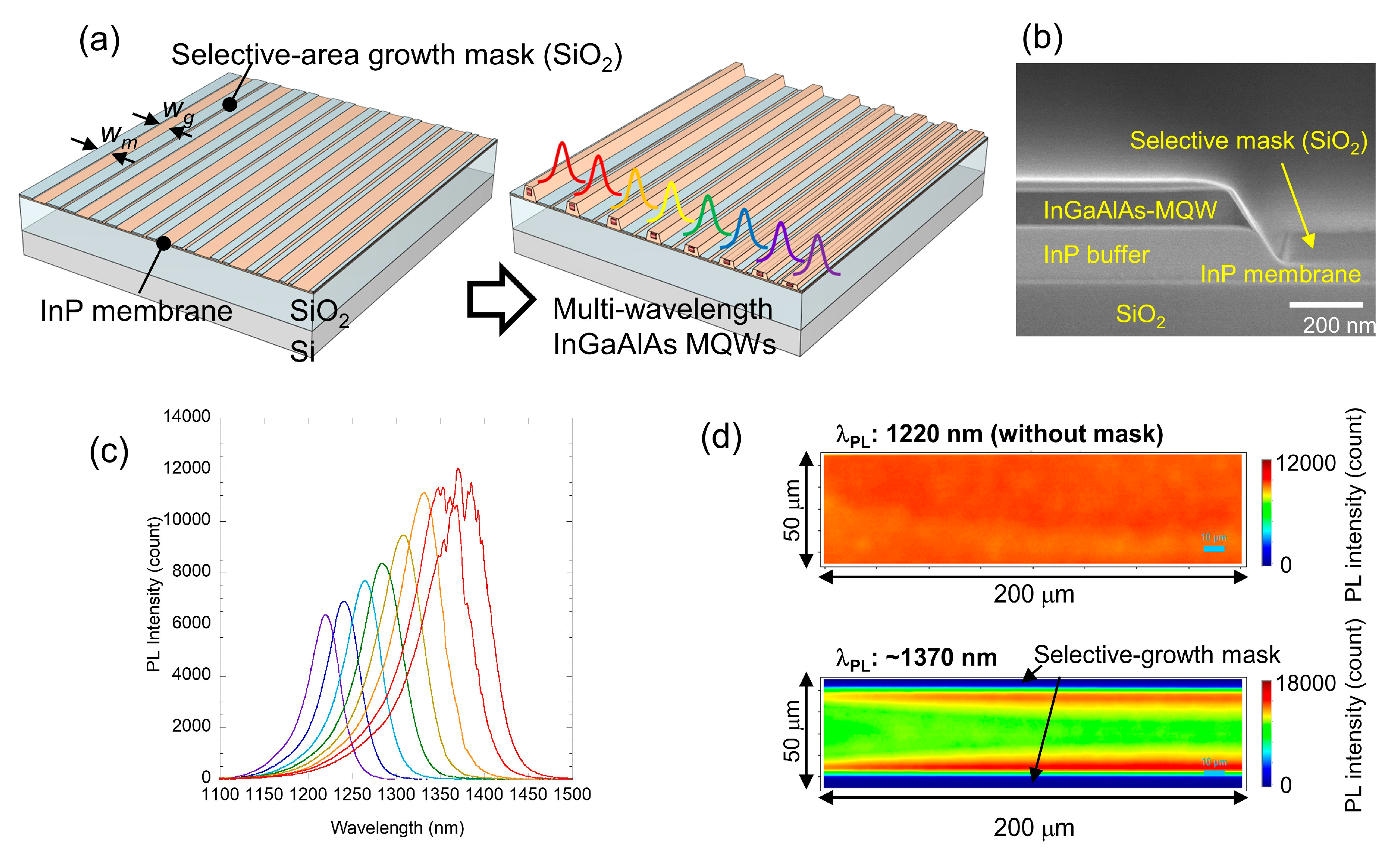
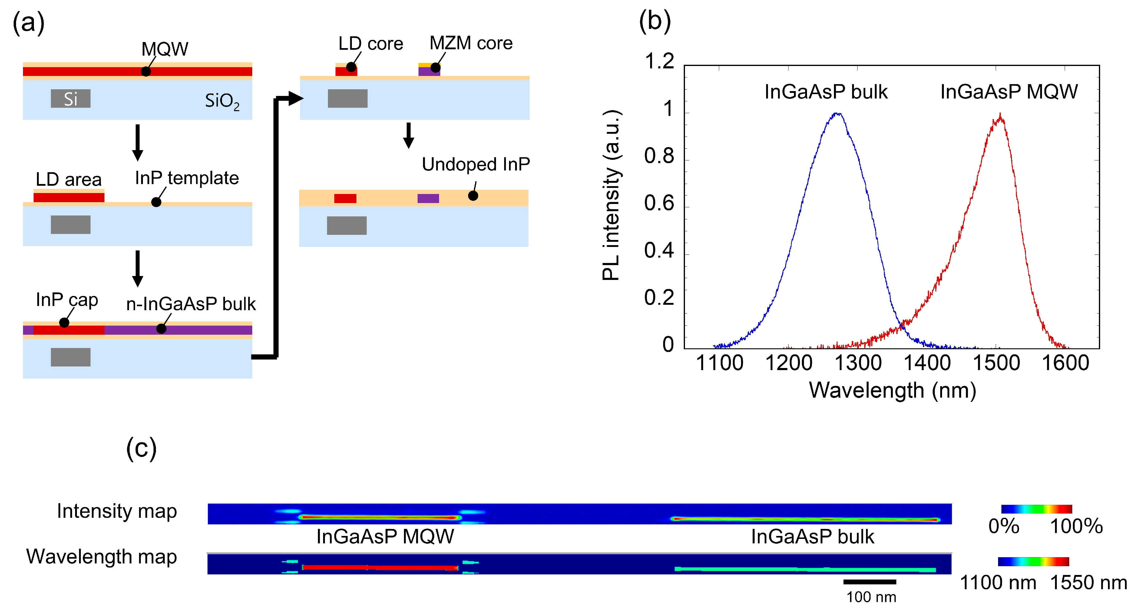
3.2.1. Multi-Wavelength Laser Array Using Selective-Area Epitaxial Growth

To support wide-wavelength range WDM systems, such as local area network (LAN) WDM or coarse WDM (CWDM), each laser in the array should be made of an MQW that has an optimized PL peak wavelength. This is because the typical full-width at half maximum of the MQW gain spectrum is ~50 nm, whereas LAN-WDM requires 35.6 nm and CWDM requires a 60- or 140-nm lasing wavelength range [73]. To integrate a WDM laser array with single epitaxy, we demonstrated the selective-area epitaxial growth of an MQW using an InP-on-insulator substrate. Figure 13a shows a schematic of the selective-area growth of the InGaAlAs MQW active layer. Due to the very high selectivity of the growth rate between the semiconductor surface and SiO2 mask, the epitaxial layer thickness and crystal composition can be controlled by changing the mask width (wm) and distance between the masks (wg), which enables us to control the bandgap of the MQW layer. Therefore, the growth of the WDM laser array with a single growth becomes possible [33,74,75]. To control the PL wavelength for CWDM application, we selectively grew InGaAlAs 6-period MQWs on an InP-on-insulator substrate with the mask width ranging from 0 to 55 μm and the distance between the masks fixed at 40 μm. The epitaxial layer consists of an InP buffer layer (~70 nm), MQW layer, and InP cap layer (~25 nm) for blanket epitaxy (without selective growth mask). Figure 13b shows a cross-sectional SEM image of an MQW selectively grown on the InP-on-insulator substrate at the vicinity of the SiO2 mask. The total III-V layer thickness with the largest mask was estimated as ~310 nm, which is less than the critical thickness determined by thermal strain. Figure 13c shows the PL spectra for eight MQWs measured with a PL microscope. Although the peak PL wavelength for the widest selective-area mask is unclear due to the H2O atmospheric absorption peaks at around 1380 nm, we obtained multiple active regions with PL peak wavelengths over ~150 nm by carrying out only one selective epitaxial growth on the InP-on-insulator substrate. We also observed uniform PL intensity with and without selective masks for a 40 × 200 μm2 area, as shown in Figure 13d, which is wide enough to fabricate active regions of lasers.
The eight-channel membrane DML array on a Si substrate was fabricated using the selectively grown MQWs [69]. We controlled the PL wavelength of the MQWs for LAN-WDM application. Figure 14a,b shows cross-sectional BF-STEM images of the selectively grown lasers on a Si substrate for the shortest wavelength channel and longest wavelength channel, respectively. Due to the different growth rate caused by selective epitaxy, each BH had a different total thickness but all were thinner than 350 nm. The lasers have a lateral-current injection structure and surface grating similar to those discussed in Section 3.1. The active-region length was 140 μm. Figure 14c shows the lasing spectra of eight channel DMLs with bias currents from 15 to 23 mA. The deviations between the designed wavelength and measured lasing wavelengths were less than 2 nm, and the mean channel spacing was 860 GHz. In addition, the wavelength detuning between the PL-peak and lasing spectra was almost constant (~35 nm) for all channels. As a result, the lasing wavelength of each channel being almost at the amplified spontaneous emission peak. This indicates precise controllability of the lasing wavelength of multi-wavelength lasers with optimal gain mediums using selective-area epitaxial growth. Finally, dynamic characteristics of the DML array were evaluated at 25 °C. We demonstrated 25.8-Gbit/s direct modulation with a 231−1 PRBS NRZ signal, and any pre-emphasis or equalization were not used. Figure 14d shows the eight-channel eye diagrams observed by a sampling oscilloscope. The bias currents were 15.0 to 26.5 mA, bias voltages were 1.84 to 2.65 V, and voltage swings were 0.89 to 1.58 Vp-p. We confirmed that all eight channels can be modulated at 25.8-Gbit/s with a dynamic extinction ratio of >4.0 dB. These results strongly indicate the potential for establishing wide-wavelength-range WDM-PICs for optical interconnects for future data-center networks using the III-V-on-insulator substrate.

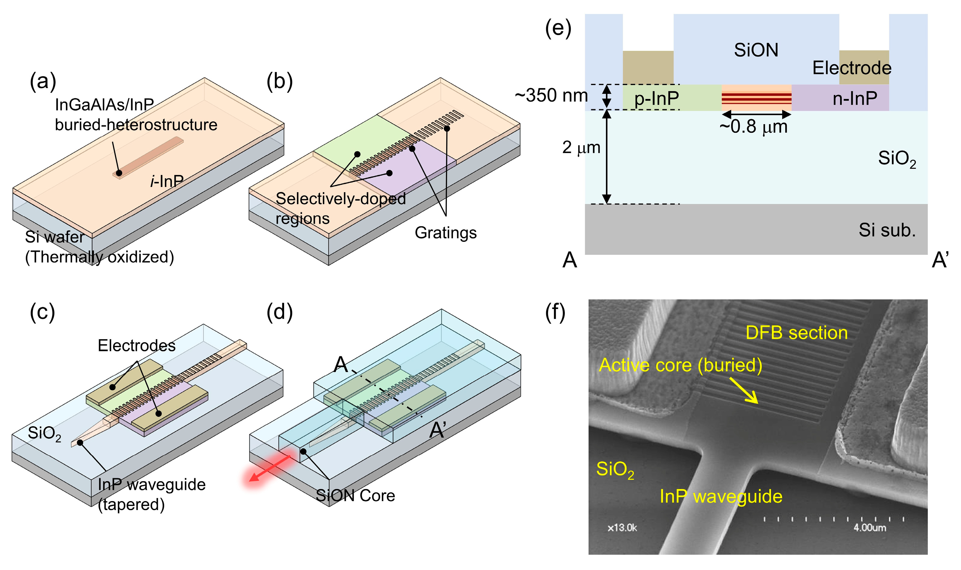
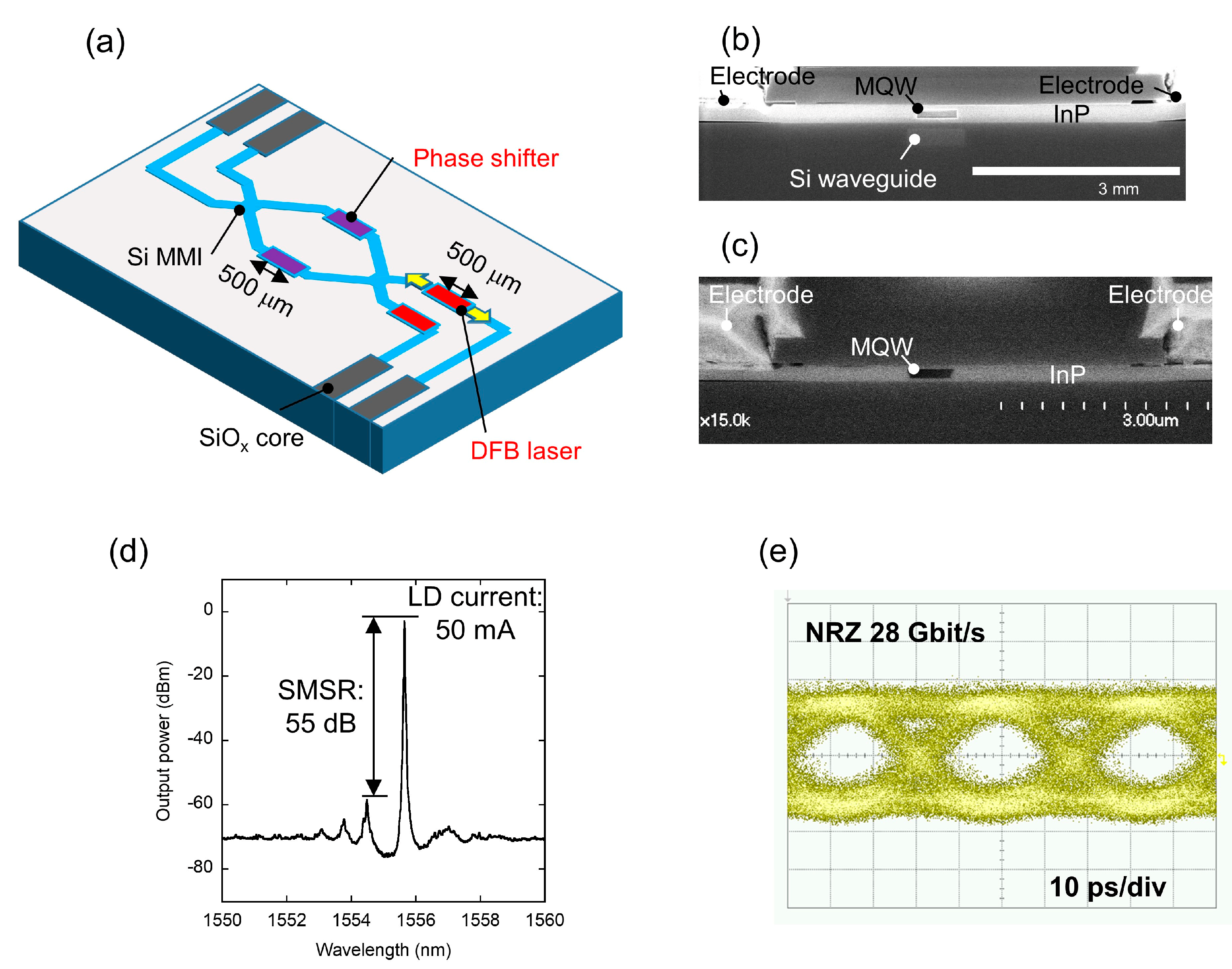
3.2.2. DFB Laser Integrated with MZM Using Epitaxial Regrowth of InGaAsP

To support advanced high-baud-rate modulation formats for data centers, a WDM transmitter PIC that includes an MZM with a distributed feedback (DFB) laser array is desirable. For this purpose, heterogeneously integrated PICs using low-loss Si photonics devices for optical multiplexer and Mach–Zehnder interferometers and III-V-based devices for laser and phase modulators are promising. Therefore, it is essential to use BJ regrowth on a III-V-on-insulator substrate, which enables the integration of different-bandgap active regions on the same plane. Figure 15a shows the process flow of integrating BHs that include different bandgap active regions [71]. A six-period InGaAsP MQW-DH optimized for DFB lasers was originally grown on an InP substrate and transferred to a Si-photonics platform using direct bonding. The 220-nm-thick Si waveguide layer was fabricated in advance underneath the MQW layer. After removing the excess MQW region, a 20-nm InP buffer layer, 100-nm-thick Si-doped InGaAsP bulk layer optimized for phase shifters, and 30-nm InP cap layer were regrown on an InP membrane. We adopted a thin InP buffer layer to obtain a high confinement factor in the membrane phase shifter (>40%) for high modulation efficiency. These two active regions were then simultaneously patterned to mesa-stripes and buried with undoped InP. The total III-V layer thickness was 230 nm, which was thinner than the critical thickness determined by thermal strain. Figure 15b shows the normalized PL spectra for two BHs measured with a PL microscope. Figure 15c shows the PL-intensity map and PL-wavelength map for the two BHs placed in close to evaluate PL at one mapping. The different bandgap materials for the C-band DFB laser (λPL: 1.52 μm), MZM (λPL: 1.3 μm) and passive InP waveguide were integrated on the Si-photonics platform. The PL signals observed at the vicinity of InGaAsP MQW corners originate from the remaining selectively grown InGaAsP bulk layer because the growth rate accelerates at these regions. The micro-PL map revealed that both the MQW-BH and InGaAsP-bulk BH were uniform, although the InGaAsP bulk layer was selectively grown on an InP-on-insulator substrate. Since the InP buffer layer was only 20 nm, this growth technique should also be applicable for BJ regrowth, which enables the fabrication of EADFB lasers.
Figure 16a shows a schematic of a DFB laser integrated with a MZM on a Si-photonic platform using our epitaxial regrowth technique. Both the DFB laser and phase shifters were 500-μm long and 230-nm thick and optically connected to the Si waveguides and Si multimode interferometers (MMIs) underneath the III-V membrane layer. The Si inverse-taper SSCs were also integrated for the low-loss fiber coupling. The lasing emission was obtained from both ends of the DFB laser, and two output waveguides were integrated so that the lasing characteristics with and without an MZM can be measured. Figure 16b,c shows cross-sectional SEM images of the fabricated chip for the DFB-laser section and phase-shifter section, respectively. The p-i-n and p-n diodes were fabricated using Zn thermal diffusion and Si ion implantation to the InP layers. Figure 16d shows the lasing spectrum of the output light measured by butt-coupling the HNAF. The laser current was 50 mA and MZM DC voltage was 4.5 V. These results indicate single-mode operation with a side-mode suppression ratio of around 55 dB. We also input radio-frequency signals to one arm of the MZM to evaluate its dynamic characteristics. Figure 16e shows the measured eye diagram for a 28-Gbit/s signal without 50-Ω termination. A clear eye opening was obtained with a laser current of 42 mA. In addition, the VπL estimated from the static Vπ measurement was around 0.4 Vcm, which is almost three times smaller than that of a conventional Si MZM [71].

4. Conclusions

In this paper, the recent progress in the epitaxial growth technique using the InP-based membrane on a Si substrate and its contribution for integrating of low-operation energy membrane photonic devices on a Si substrate have been reviewed. Use of the thin III-V membrane structure makes it possible to carry out high-quality epitaxial growth on an InP-on-insulator substrate. The thickness-dependence of the high-temperature tolerance of a III-V-on-insulator substrate was revealed both theoretically and experimentally. In addition, the growth of quaternary compound semiconductors such as InGaAlAs MQWs and InGaAsP bulk on an InP-on-insulator substrate was demonstrated. The TDD in InGaAlAs MQWs evaluated with a PL microscope was less than 4.0 × 10²/cm2, which is even lower than the typical commercially available InP wafer specification. TEM measurement also revealed that there is no obvious structural degradation in MQWs grown on an InP-on-insulator substrate. Using this growth technique, a 1.3-μm-range directly modulated laser array on a Si substrate was fabricated. The fabricated laser array exhibited 25.8-Gbit/s direct modulation at 50 °C with bias currents from only 8.0 to 8.3 mA and lasted up to 95 °C. In addition, a multi-wavelength DML array with optimized-bandgap MQWs was demonstrated using the selective-area growth of multi-wavelength MQWs on an InP-on-insulator substrate. Selective-area growth enables full-O-band bandgap control of InGaAlAs MQWs over 150 nm. Furthermore, integration of a DFB laser and InGaAsP MZM was demonstrated using selective regrowth of InGaAsP bulk material on the InP membrane on Si-photonics circuits.
To manufacture PICs using epitaxial regrowth techniques, demonstrating scalability will be the next important step. There is essentially no difficulty up to 150-mm wafer because both the InP wafer and MOVPE system are already available. To integrate InP on 200- and 300-mm Si wafer, die-to-wafer bonding technologies can resolve the wafer-size mismatch between Si and InP [76]. In addition, Smart Cut and epitaxial lift-off are promising technologies to fabricate InP-on-insulator substrate at low cost because these technologies enable reuse of the donor InP wafer [77,78]. We believe that the epitaxial growth techniques using an InP-on-insulator substrate are scalable and paving the way for providing a promising approach for establishing III-V/Si PICs for future data-center networks.

Author Contributions

Conceptualization, S.M.; methodology, T.F., T.H., T.S. and S.M.; software, K.T. and T.K.; validation, T.F., T.H., T.A., H.N., K.T., T.S. and T.T.; formal analysis, T.K.; investigation, T.F., T.H., T.A., H.N., K.T., T.S. and T.T; writing—original draft preparation, T.F.; writing—review and editing, S.M.; visualization, T.F.; supervision, S.M.; project administration, S.M. All authors have read and agreed to the published version of the manuscript.

Funding

This research received no external funding.

Institutional Review Board Statement

Not applicable.

Informed Consent Statement

Not applicable.

Data Availability Statement

The data that support the findings of this study are available from the corresponding author upon reasonable request.

Acknowledgments

The authors thank Y. Kawaguchi, M. Kiuchi, K. Ishibashi, Y. Shouji, and Y. Yokoyama for their great help with device fabrication. The authors also thank H. Fukuda for his valuable suggestions and fruitful discussions.

Conflicts of Interest

The authors declare no conflict of interest.

References

  1. Chen, X.; Li, C.; Tsang, H.K. Device engineering for silicon photonics. NPG Asia Mater. 2011, 3, 34–40. [Google Scholar] [CrossRef] [Green Version]
  2. Rickman, A. The commercialization of silicon photonics. Nat. Photonics 2014, 8, 579–582. [Google Scholar] [CrossRef]
  3. Nagarajan, R.; Joyner, C.H.; Schneider, R.P.; Bostak, J.S.; Butrie, T.; Dentai, A.G.; Dominic, V.G.; Evans, P.W.; Kato, M.; Kauffman, M.; et al. Large-scale photonic integrated circuits. IEEE J. Sel. Top. Quantum Electron. 2005, 11, 50–65. [Google Scholar] [CrossRef]
  4. Komljenovic, T.; Davenport, M.; Hulme, J.; Liu, A.Y.; Santis, C.T.; Spott, A.; Srinivasan, S.; Stanton, E.J.; Zhang, C.; Bowers, J.E. Heterogeneous Silicon Photonic Integrated Circuits. J. Light. Technol. 2016, 34, 20–35. [Google Scholar] [CrossRef]
  5. Dong, P.; Liu, X.; Chandrasekhar, S.; Buhl, L.L.; Aroca, R.; Chen, Y.-K. Monolithic Silicon Photonic Integrated Circuits for Compact 100+Gb/s Coherent Optical Receivers and Transmitters. IEEE J. Sel. Top. Quantum Electron. 2014, 20, 150–157. [Google Scholar] [CrossRef]
  6. Horikawa, T.; Shimura, D.; Okayama, H.; Jeong, S.-H.; Takahashi, H.; Ushida, J.; Sobu, Y.; Shiina, A.; Tokushima, M.; Kinoshita, K.; et al. A 300-mm Silicon Photonics Platform for Large-Scale Device Integration. IEEE J. Sel. Top. Quantum Electron. 2018, 24, 1–15. [Google Scholar] [CrossRef]
  7. Tsuchizawa, T.; Yamada, K.; Fukuda, H.; Watanabe, T.; Takahashi, J.; Takahashi, M.; Shoji, T.; Tamechika, E.; Itabashi, S.; Morita, H. Microphotonics devices based on silicon microfabrication technology. IEEE J. Sel. Top. Quantum Electron. 2005, 11, 232–240. [Google Scholar] [CrossRef]
  8. Arakawa, Y.; Nakamura, T.; Urino, Y.; Fujita, T. Silicon photonics for next generation system integration platform. IEEE Commun. Mag. 2013, 51, 72–77. [Google Scholar] [CrossRef]
  9. Thomson, D.; Zilkie, A.; Bowers, J.E.; Komljenovic, T.; Reed, G.T.; Vivien, L.; Marris-Morini, D.; Cassan, E.; Virot, L.; Fédéli, J.M.; et al. Roadmap on silicon photonics. J. Opt. 2016, 18, 1–20. [Google Scholar] [CrossRef]
  10. Miller, D. Device Requirements for Optical Interconnects to Silicon Chips. Proc. IEEE 2009, 97, 1166–1185. [Google Scholar] [CrossRef] [Green Version]
  11. Kobayashi, W.; Ito, T.; Yamanaka, T.; Fujisawa, T.; Shibata, Y.; Kurosaki, T.; Kohtoku, M.; Tadokoro, T.; Sanjoh, H. 50-Gb/s Direct Modulation of a 1.3-μm InGaAlAs-Based DFB Laser With a Ridge Waveguide Structure. IEEE J. Sel. Top. Quantum Electron. 2013, 19, 1500908. [Google Scholar] [CrossRef]
  12. Nakahara, K.; Wakayama, Y.; Kitatani, T.; Taniguchi, T.; Fukamachi, T.; Sakuma, Y.; Tanaka, S. Direct Modulation at 56 and 50 Gb/s of 1.3-μm InGaAlAs Ridge-Shaped-BH DFB Lasers. IEEE Photonics Technol. Lett. 2015, 27, 534–536. [Google Scholar] [CrossRef]
  13. Nakahara, K.; Tsuchiya, T.; Kitatani, T.; Shinoda, K.; Taniguchi, T.; Fujisaki, S.; Kikawa, T.; Nomoto, E.; Hamano, F.; Sawada, M.; et al. 1.3-μm InGaAlAs directly modulated MQW RWG DFB lasers operating over 10 Gb/s and 100 °C. In Proceedings of the Optical Fiber Communication Conference (OFC), Los Angeles, CA, USA, 22 February 2004; Available online: https://www.osapublishing.org/abstract.cfm?URI=OFC-2004-ThD1 (accessed on 18 January 2021).
  14. Fujisawa, T.; Kanazawa, S.; Takahata, K.; Kobayashi, W.; Tadokoro, T.; Ishii, H.; Kano, F. 1.3-μm, 4 × 25-Gbit/s, EADFB laser array module with large-output-power and low-driving-voltage for energy-efficient 100GbE transmitter. Opt. Express 2012, 20, 614. [Google Scholar] [CrossRef] [PubMed]
  15. Takeuchi, H.; Tsuzuki, K.; Sato, K.; Yamamoto, M.; Itaya, Y.; Sano, A.; Yoneyama, M.; Otsuji, T. Very high-speed light-source module up to 40 Gb/s containing an MQW electroabsorption modulator integrated with a DFB laser. IEEE J. Sel. Top. Quantum Electron. 1997, 3, 336–343. [Google Scholar] [CrossRef]
  16. Kawamura, Y.; Wakita, K.; Yoshikuni, Y.; Itaya, Y.; Asahi, H. Monolithic Integration of a DFB Laser and an MQW Optical Modulator in the 1.5 µm Wavelength Range. IEEE J. Quantum Electron. 1987, 23, 915–918. [Google Scholar] [CrossRef]
  17. Griffin, R.A.; Jones, S.K.; Whitbread, N.; Heck, S.C.; Langley, L.N. InP Mach–Zehnder Modulator Platform for 10/40/100/200-Gb/s Operation. IEEE J. Sel. Top. Quantum Electron. 2013, 19, 158–166. [Google Scholar] [CrossRef]
  18. Ogiso, Y.; Ozaki, J.; Kashio, N.; Kikuchi, N.; Tanobe, H.; Ohiso, Y.; Kohtoku, M. 100 Gb/s and 2 V Vπ InP Mach-Zehnder modulator with an n-i-p-n heterostructure. Electron. Lett. 2016, 52, 1866–1867. [Google Scholar] [CrossRef]
  19. Justice, J.; Bower, C.; Meitl, M.; Mooney, M.B.; Gubbins, M.A.; Corbett, B. Wafer-scale integration of group III-V lasers on silicon using transfer printing of epitaxial layers. Nat. Photonics 2012, 6, 610–614. [Google Scholar] [CrossRef]
  20. Roelkens, G.; Abassi, A.; Cardile, P.; Dave, U.; de Groote, A.; de Koninck, Y.; Dhoore, S.; Fu, X.; Gassenq, A.; Hattasan, N.; et al. III-V-on-Silicon Photonic Devices for Optical Communication and Sensing. Photonics 2015, 2, 969–1004. [Google Scholar] [CrossRef] [Green Version]
  21. Jones, R.; Doussiere, P.; Driscoll, J.B.; Lin, W.; Yu, H.; Akulova, Y.; Komljenovic, T.; Bowers, J.E. Heterogeneously Integrated InP/Silicon Photonics: Fabricating Fully Functional Transceivers. IEEE Nanotechnol. Mag. 2019, 13, 17–26. [Google Scholar] [CrossRef]
  22. Ramirez, J.M.; Malhouitre, S.; Gradkowski, K.; Morrissey, P.E.; O’Brien, P.; Caillaud, C.; Vaissiere, N.; Decobert, J.; Lei, S.; Enright, R.; et al. III-V-on-Silicon Integration: From Hybrid Devices to Heterogeneous Photonic Integrated Circuits. IEEE J. Sel. Top. Quantum Electron. 2020, 26, 1–13. [Google Scholar] [CrossRef]
  23. Sugo, M.; Mori, H.; Tachikawa, M.; Itoh, Y.; Yamamoto, M. Room-temperature operation of an InGaAsP double-heterostructure laser emitting at 1.55 μm on a Si substrate. Appl. Phys. Lett. 1990, 57, 593–595. [Google Scholar] [CrossRef]
  24. Shi, B.; Zhao, H.; Wang, L.; Song, B.; Suran Brunelli, S.T.; Klamkin, J. Continuous-wave electrically pumped 1550 nm lasers epitaxially grown on on-axis (001) silicon. Optica 2019, 6, 1507. [Google Scholar] [CrossRef]
  25. Megalini, L.; Bonef, B.; Cabinian, B.C.; Zhao, H.; Taylor, A.; Speck, J.S.; Bowers, J.E.; Klamkin, J. 1550-nm InGaAsP multi-quantum-well structures selectively grown on v-groove-patterned SOI substrates. Appl. Phys. Lett. 2017, 111, 032105. [Google Scholar] [CrossRef]
  26. Chen, S.; Li, W.; Wu, J.; Jiang, Q.; Tang, M.; Shutts, S.; Elliott, S.N.; Sobiesierski, A.; Seeds, A.J.; Ross, I.; et al. Electrically pumped continuous-wave III-V quantum dot lasers on silicon. Nat. Photonics 2016, 10, 307–311. [Google Scholar] [CrossRef]
  27. Liu, A.Y.; Peters, J.; Huang, X.; Jung, D.; Norman, J.; Lee, M.L.; Gossard, A.C.; Bowers, J.E. Electrically pumped continuous-wave 1.3 μm quantum-dot lasers epitaxially grown on on-axis (001) GaP/Si. Opt. Lett. 2017, 42, 338. [Google Scholar] [CrossRef]
  28. Schmid, H.; Borg, M.; Moselund, K.; Gignac, L.; Breslin, C.M.; Bruley, J.; Cutaia, D.; Riel, H. Template-assisted selective epitaxy of III–V nanoscale devices for co-planar heterogeneous integration with Si. Appl. Phys. Lett. 2015, 106, 233101. [Google Scholar] [CrossRef]
  29. Czornomaz, L.; Uccelli, E.; Sousa, M.; Deshpande, V.; Djara, V.; Caimi, D.; Rossell, M.D.; Erni, R.; Fompeyrine, J. Confined Epitaxial Lateral Overgrowth (CELO): A novel concept for scalable integration of CMOS-compatible InGaAs-on-insulator MOSFETs on large-area Si substrates. In Proceedings of the Symposium on VLSI Technology, Kyoto, Japan, 16–18 June 2015; Volume 2015-Augus, pp. T172–T173. [Google Scholar]
  30. Wang, Z.; Tian, B.; Pantouvaki, M.; Guo, W.; Absil, P.; Van Campenhout, J.; Merckling, C.; Van Thourhout, D. Room-temperature InP distributed feedback laser array directly grown on silicon. Nat. Photonics 2015, 9, 837–842. [Google Scholar] [CrossRef] [Green Version]
  31. Mayer, B.F.; Wirths, S.; Mauthe, S.; Staudinger, P.; Sousa, M.; Winiger, J.; Schmid, H.; Moselund, K.E. Microcavity Lasers on Silicon by Template-Assisted Selective Epitaxy of Microsubstrates. IEEE Photonics Technol. Lett. 2019, 31, 1021–1024. [Google Scholar] [CrossRef]
  32. Han, Y.; Yan, Z.; Ng, W.K.; Xue, Y.; Wong, K.S.; Lau, K.M. Bufferless 1.5 µm III-V lasers grown on Si-photonics 220 nm silicon-on-insulator platforms. Optica 2020, 7, 148. [Google Scholar] [CrossRef]
  33. Sasaki, T.; Kitamura, M.; Mito, I. Selective metalorganic vapor phase epitaxial growth of InGaAsP/InP layers with bandgap energy control in InGaAs/InGaAsP multiple-quantum well structures. J. Cryst. Growth 1993, 132, 435–443. [Google Scholar] [CrossRef]
  34. Tanabe, K.; Watanabe, K.; Arakawa, Y. III-V/Si hybrid photonic devices by direct fusion bonding. Sci. Rep. 2012, 2, 349. [Google Scholar] [CrossRef] [PubMed]
  35. Matsuo, S.; Tateno, K.; Nakahara, T.; Tsuda, H.; Kurokawa, T. Use of polyimide bonding for hybrid integration of a vertical cavity surface emitting laser on a silicon substrate. Electron. Lett. 1997, 33, 1148. [Google Scholar] [CrossRef]
  36. Fang, A.W.; Park, H.; Cohen, O.; Jones, R.; Paniccia, M.J.; Bowers, J.E. Electrically pumped hybrid AlGaInAs-silicon evanescent laser. Opt. Express 2006, 14, 9203. [Google Scholar] [CrossRef] [PubMed]
  37. Komljenovic, T.; Srinivasan, S.; Norberg, E.; Davenport, M.; Fish, G.; Bowers, J.E. Widely Tunable Narrow-Linewidth Monolithically Integrated External-Cavity Semiconductor Lasers. IEEE J. Sel. Top. Quantum Electron. 2015, 21, 214–222. [Google Scholar] [CrossRef]
  38. Keyvaninia, S.; Verstuyft, S.; Van Landschoot, L.; Lelarge, F.; Duan, G.-H.; Messaoudene, S.; Fedeli, J.M.; De Vries, T.; Smalbrugge, B.; Geluk, E.J.; et al. Heterogeneously integrated III-V/silicon distributed feedback lasers. Opt. Lett. 2013, 38, 5434. [Google Scholar] [CrossRef] [PubMed] [Green Version]
  39. Loi, R.; O’Callaghan, J.; Roycroft, B.; Robert, C.; Fecioru, A.; Trindade, A.J.; Gocalinska, A.; Pelucchi, E.; Bower, C.A.; Corbett, B. Transfer Printing of AlGaInAs/InP Etched Facet Lasers to Si Substrates. IEEE Photonics J. 2016, 8, 1–10. [Google Scholar] [CrossRef]
  40. Katsumi, R.; Ota, Y.; Kakuda, M.; Iwamoto, S.; Arakawa, Y. Transfer-printed single-photon sources coupled to wire waveguides. Optica 2018, 5, 691. [Google Scholar] [CrossRef] [Green Version]
  41. Yang, H.; Zhao, D.; Chuwongin, S.; Seo, J.-H.; Yang, W.; Shuai, Y.; Berggren, J.; Hammar, M.; Ma, Z.; Zhou, W. Transfer-printed stacked nanomembrane lasers on silicon. Nat. Photonics 2012, 6, 615–620. [Google Scholar] [CrossRef]
  42. Dutta, N.K.; Zilko, J.L.; Cella, T.; Ackerman, D.A.; Shen, T.M.; Napholtz, S.G. InGaAsP laser with semi-insulating current confining layers. Appl. Phys. Lett. 1986, 48, 1572–1573. [Google Scholar] [CrossRef]
  43. Matsuo, S.; Shinya, A.; Kakitsuka, T.; Nozaki, K.; Segawa, T.; Sato, T.; Kawaguchi, Y.; Notomi, M. High-speed ultracompact buried heterostructure photonic-crystal laser with 13 fJ of energy consumed per bit transmitted. Nat. Photonics 2010, 4, 648–654. [Google Scholar] [CrossRef]
  44. Fontcuberta i Morral, A.; Zahler, J.M.; Atwater, H.A.; Ahrenkiel, S.P.; Wanlass, M.W. InGaAs/InP double heterostructures on InP/Si templates fabricated by wafer bonding and hydrogen-induced exfoliation. Appl. Phys. Lett. 2003, 83, 5413. [Google Scholar] [CrossRef] [Green Version]
  45. Matsuo, S.; Fujii, T.; Hasebe, K.; Takeda, K.; Sato, T.; Kakitsuka, T. Directly modulated buried heterostructure DFB laser on SiO2/Si substrate fabricated by regrowth of InP using bonded active layer. Opt. Express 2014, 22, 12139. [Google Scholar] [CrossRef] [PubMed]
  46. Fujii, T.; Sato, T.; Takeda, K.; Hasebe, K.; Kakitsuka, T.; Matsuo, S. Epitaxial growth of InP to bury directly bonded thin active layer on SiO2/Si substrate for fabricating distributed feedback lasers on silicon. IET Optoelectron. 2015, 9, 151–157. [Google Scholar] [CrossRef]
  47. Fujii, T.; Nishi, H.; Takeda, K.; Kanno, E.; Hasebe, K.; Kakitsuka, T.; Yamamoto, T.; Fukuda, H.; Tsuchizawa, T.; Matsuo, S. 1.3-µm Directly Modulated Membrane Laser Array Employing Epitaxial Growth of InGaAlAs MQW on InP/SiO2/Si Substrate. In Proceedings of the European Conference on Optical Communication (ECOC), Düsseldorf, Germany, 18–22 September 2016. [Google Scholar]
  48. Matsumoto, K.; Kishikawa, J.; Nishiyama, T.; Onuki, Y.; Shimomura, K. Novel integration method for III–V semiconductor devices on silicon platform. Jpn. J. Appl. Phys. 2016, 55, 112201. [Google Scholar] [CrossRef]
  49. Matsuo, S.; Kakitsuka, T. Low-operating-energy directly modulated lasers for short-distance optical interconnects. Adv. Opt. Photonics 2018, 10, 567. [Google Scholar] [CrossRef]
  50. Baumgartner, Y.; Caer, C.; Seifried, M.; Villares, G.; Caimi, D.; Morf, T.; Faist, J.; Offrein, B.J.; Czornomaz, L. CMOS-Compatible Hybrid III-V/Si Photodiodes Using a Lateral Current Collection Scheme. In Proceedings of the European Conference on Optical Communication (ECOC), Rome, Italy, 23–27 September 2018. Th1C.5. [Google Scholar]
  51. Hu, Y.; Liang, D.; Mukherjee, K.; Li, Y.; Zhang, C.; Kurczveil, G.; Huang, X.; Beausoleil, R.G. III/V-on-Si MQW lasers by using a novel photonic integration method of regrowth on a bonding template. Light Sci. Appl. 2019, 8, 93. [Google Scholar] [CrossRef]
  52. Besancon, C.; Vaissiere, N.; Dupré, C.; Fournel, F.; Sanchez, L.; Jany, C.; David, S.; Bassani, F.; Baron, T.; Decobert, J. Epitaxial Growth of High-Quality AlGaInAs-Based Active Structures on a Directly Bonded InP-SiO2/Si Substrate. Phys. Status Solidi 2020, 217, 1900523. [Google Scholar] [CrossRef]
  53. Kobayashi, W.; Arai, M.; Yamanaka, T.; Fujiwara, N.; Fujisawa, T.; Tadokoro, T.; Tsuzuki, K.; Kondo, Y.; Kano, F. Design and fabrication of 10-/40-Gb/s, uncooled electroabsorption modulator integrated DFB laser with butt-joint structure. J. Light. Technol. 2010, 28, 164–171. [Google Scholar] [CrossRef]
  54. Van de Leur, R.H.M.; Schellingerhout, A.J.G.; Tuinstra, F.; Mooij, J.E. Critical thickness for pseudomorphic growth of Si/Ge alloys and superlattices. J. Appl. Phys. 1988, 64, 3043–3050. [Google Scholar] [CrossRef]
  55. Adachi, S. Properties of Indium Phosphide; INSPEC: London, UK, 1991; ISBN 086341642X. [Google Scholar]
  56. Sato, T.; Kondo, Y.; Sekiguchi, T.; Suemasu, T. Sb Surfactant Effect on Defect Evolution in Compressively Strained In0.80Ga0.20As Quantum Well on InP Grown by Metalorganic Vapor Phase Epitaxy. Appl. Phys. Express 2008, 1, 111202. [Google Scholar] [CrossRef]
  57. Matthews, J.W.; Blakeslee, A.E. Defects in epitaxial multilayers. J. Cryst. Growth 1974, 27, 118–125. [Google Scholar] [CrossRef]
  58. Liang, D.; Roelkens, G.; Baets, R.; Bowers, J. Hybrid Integrated Platforms for Silicon Photonics. Materials 2010, 3, 1782–1802. [Google Scholar] [CrossRef] [Green Version]
  59. Adachi, S.; Noguchi, Y.; Kawaguchi, H. Chemical Etching of InGaAsP/InP DH Wafer. J. Electrochem. Soc. 1982, 129, 1053–1062. [Google Scholar] [CrossRef]
  60. Fujii, T.; Takeda, K.; Diamantopoulos, N.-P.; Kanno, E.; Hasebe, K.; Nishi, H.; Nakao, R.; Kakitsuka, T.; Matsuo, S. Heterogeneously Integrated Membrane Lasers on Si Substrate for Low Operating Energy Optical Links. IEEE J. Sel. Top. Quantum Electron. 2018, 24, 1–8. [Google Scholar] [CrossRef]
  61. Stano, A. Chemical Etching Characteristics of InGaAs/InP and InAlAs/InP Heterostructures. J. Electrochem. Soc. 1987, 134, 448–452. [Google Scholar] [CrossRef]
  62. Tong, M.; Nummila, K.; Ketterson, A.A.; Adesida, I.; Aina, L.; Mattingly, M. Selective Wet Etching Characteristics of Lattice-Matched InGaAs/InAlAs/InP. J. Electrochem. Soc. 1992, 139, L91–L93. [Google Scholar] [CrossRef]
  63. Matsui, Y.; Schatz, R.; Pham, T.; Ling, W.A.; Carey, G.; Daghighian, H.M.; Adams, D.; Sudo, T.; Roxlo, C. 55 GHz Bandwidth Distributed Reflector Laser. J. Light. Technol. 2017, 35, 397–403. [Google Scholar] [CrossRef]
  64. Sasada, N.; Nakajima, T.; Sekino, Y.; Nakanishi, A.; Mukaikubo, M.; Ebisu, M.; Mitaki, M.; Hayakawa, S.; Naoe, K. Wide-Temperature-Range (25–80 °C) 53-Gbaud PAM4 (106-Gb/s) Operation of 1.3-μm Directly Modulated DFB Lasers for 10-km Transmission. J. Light. Technol. 2019, 37, 1686–1689. [Google Scholar] [CrossRef]
  65. Nakai, Y.; Nakanishi, A.; Yamaguchi, Y.; Yamauchi, S.; Nakamura, A.; Asakura, H.; Takita, H.; Hayakawa, S.; Mitaki, M.; Sakuma, Y.; et al. Uncooled Operation of 53-GBd PAM4 (106-Gb/s) EA/DFB Lasers With Extremely Low Drive Voltage With 0.9 V pp. J. Light. Technol. 2019, 37, 1658–1662. [Google Scholar] [CrossRef]
  66. Yamaoka, S.; Diamantopoulos, N.-P.; Nishi, H.; Nakao, R.; Fujii, T.; Takeda, K.; Hiraki, T.; Tsurugaya, T.; Kanazawa, S.; Tanobe, H.; et al. Directly modulated membrane lasers with 108 GHz bandwidth on a high-thermal-conductivity silicon carbide substrate. Nat. Photonics 2021, 15, 28–35. [Google Scholar] [CrossRef]
  67. Fujii, T.; Takeda, K.; Kanno, E.; Nishi, H.; Hasebe, K.; Yamamoto, T.; Kakitsuka, T.; Matsuo, S. Growth of InGaAsP-based MQW layer on InP template bonded to Si substrate for fabricating membrane lasers. In Proceedings of the Compound Semiconductor Week (CSW), Toyama, Japan, 26–30 June 2016. TuD3-2. [Google Scholar]
  68. Fujii, T.; Takeda, K.; Kanno, E.; Hasebe, K.; Nishi, H.; Yamamoto, T.; Kakitsuka, T.; Matsuo, S. Heterogeneously integrated lasers using epitaxially grown III-V active layer on directly bonded InP/SiO2/Si substrate. In Proceedings of the IEEE Photonics Conference (IPC), Hawaii, HI, USA, 2–6 October 2016; pp. 540–541. [Google Scholar]
  69. Fujii, T.; Takeda, K.; Nishi, H.; Diamantopoulos, N.-P.; Sato, T.; Kakitsuka, T.; Tsuchizawa, T.; Matsuo, S. Multiwavelength membrane laser array using selective area growth on directly bonded InP on SiO2/Si. Optica 2020, 7, 838. [Google Scholar] [CrossRef]
  70. Hiraki, T.; Aihara, T.; Takeda, K.; Fujii, T.; Kakitsuka, T.; Tsuchizawa, T.; Fukuda, H.; Matsuo, S. Membrane InGaAsP Mach-Zehnder modulator with SiN:D waveguides on Si platform. Opt. Express 2019, 27, 18612. [Google Scholar] [CrossRef]
  71. Hiraki, T.; Aihara, T.; Fujii, T.; Takeda, K.; Kakitsuka, T.; Tsuchizawa, T.; Matsuo, S. Integrated DFB Laser Diode and High-efficiency Mach-Zehnder Modulator using Membrane III-V Semiconductors on Si Photonics Platform. In Proceedings of the IEEE International Electron Devices Meeting (IEDM), San Francisco, CA, USA, 7–11 December 2019; pp. 787–790. [Google Scholar]
  72. Fujii, T.; Nishi, H.; Takeda, K.; Kanno, E.; Hasebe, K.; Sato, T.; Kakitsuka, T.; Fukuda, H.; Tsuchizawa, T.; Matsuo, S. Temperature Characteristics of 1.3-μm Membrane Lasers on InP-on-Insulator Substrate. In Proceedings of the IEEE International Semiconductor Laser Conference (ISLC), Santa Fe, NM, USA, 16–19 September 2018. TuB8. [Google Scholar]
  73. IEEE 802.3 bs. IEEE Standard for Ethernet-Amendment 10: Media Access Control Parameters, Physical Layers, and Management Parameters for 200 Gb/s and 400 Gb/s Operation. 2017. ISBN 9781504444507. Available online: https://standards.ieee.org/standard/802_3bs-2017.html (accessed on 18 January 2021).
  74. Kudo, K.; Furushima, Y.; Nakazaki, T.; Yamaguchi, M. Densely arrayed eight-wavelength semiconductor lasers fabricated by microarray selective epitaxy. IEEE J. Sel. Top. Quantum Electron. 1999, 5, 428–434. [Google Scholar] [CrossRef]
  75. Sirenko, A.A.; Kazimirov, A.; Huang, R.; Bilderback, D.H.; O’Malley, S.; Gupta, V.; Bacher, K.; Ketelsen, L.J.P.; Ougazzaden, A. Microbeam high-resolution x-ray diffraction in strained InGaAlAs-based multiple quantum well laser structures grown selectively on masked InP substrates. J. Appl. Phys. 2005, 97, 1–7. [Google Scholar] [CrossRef] [Green Version]
  76. Sanchez, L.; Bally, L.; Montmayeul, B.; Fournel, F.; Dafonseca, J.; Augendre, E.; Di Cioccio, L.; Carron, V.; Signamarcheix, T.; Taibi, R.; et al. Chip to wafer direct bonding technologies for high density 3D integration. In Proceedings of the 2012 IEEE 62nd Electronic Components and Technology Conference, San Diego, CA, USA, 29 May–1 June 2012; pp. 1960–1964. [Google Scholar]
  77. Yablonovitch, E.; Gmitter, T.; Harbison, J.P.; Bhat, R. Extreme selectivity in the lift-off of epitaxial GaAs films. Appl. Phys. Lett. 1987, 51, 2222–2224. [Google Scholar] [CrossRef]
  78. Aspar, B.; Jalaguier, E.; Mas, A.; Locatelli, C.; Rayssac, O.; Moriceau, H.; Pocas, S.; Papon, A.M.; Michaud, J.F.; Bruel, M. Smart-Cut® process using metallic bonding: Application to transfer of Si, GaAs, InP thin films. Electron. Lett. 1999, 35, 1024. [Google Scholar] [CrossRef]
Figure 1. Process flow of fabricating membrane photonic devices on Si using epitaxial growth technique on a III-V-on-insulator platform.
Applsci 11 01801 g001
Figure 2. Strain dependence on calculated critical thickness of indium phosphide (InP) directly bonded on Si.
Applsci 11 01801 g002
Figure 3. (a) Process flow of fabricating a multi-quantum well (MQW)-double-heterostructure (DH) on SiO2/Si substrate; (b) photoluminescence (PL) intensity map for 2-inch 250-nm-thick MQW-DH transferred to SiO2/Si substrate.
Applsci 11 01801 g003
Figure 4. (ac) PL spectra for MQW-DHs with different total thicknesses on SiO2/Si substrates before (solid lines) and after (dashed lines) annealing; (df) PL-intensity map measured with PL microscope after annealing.
Applsci 11 01801 g004
Figure 5. (ac) Process flow of fabricating buried-heterostructure (BH) using MQW-DH on SiO2/Si substrate; (d) cross-sectional SEM image of BH on SiO2/Si substrate; (e) atomic force microscope (AFM) image of surface of InP membrane on SiO2/Si substrate after epitaxial growth.
Applsci 11 01801 g005
Figure 6. (a) PL spectra of indium-gallium-aluminum arsenide (InGaAlAs) MQW grown on InP-on-insulator substrate and same MQW grown on standard InP substrate; (b) PL-intensity map for MQW grown on InP-on-insulator substrate measured with PL microscope; (c) PL intensity-map for MQW-BH after regrowth of InP layer.
Applsci 11 01801 g006
Figure 7. (a) Cross-sectional bright-field scanning transmission electron microscope (BF-STEM) image of BH on Si substrate; (b,c) high-angle annular dark-field (HAADF)-STEM image of MQW-BH grown on InP-on-insulator substrate and MQW grown on InP substrate; (d,e) moving average of contrast profile extracted from HAADF-STEM images.
Applsci 11 01801 g007
Figure 8. (a) Cross-sectional energy dispersive X-ray spectrometry (EDX) map of MQW-BH on InP-on-insulator substrate; (b) extracted line profile along depth direction.
Applsci 11 01801 g008
Figure 9. (ad) Fabrication procedure of membrane distributed reflector (DR) laser using InGaAlAs MQWs grown on InP-on-insulator substrate; (e) schematic of cross-section of DR laser; (f) bird’s eye view of laser before integration of the spot-size converter (SSC).
Applsci 11 01801 g009
Figure 10. (a) Photograph of diced wafer that includes 4 8-channel laser arrays, together with top-view photograph of one 8-channel laser array; (b) bias-current dependence of optical output power and bias voltages at 25 °C; (c) lasing spectra with bias current of 4 mA at 25 °C.
Applsci 11 01801 g010
Figure 11. (a) Eye diagrams for directly modulated lasers (DMLs) with 25.8-Gbit/s non-return-to-zero (NRZ) signals at 50 °C; (b) bit-error-rates (BER) characteristics of back-to-back (BTB) and after 10-km transmissions at 50 °C.
Applsci 11 01801 g011
Figure 12. (a) Lasing spectra of two membrane lasers with different grating pitches; (b,c) temperature dependence of optical output vs. injection current for 32.1- and 39.9-nm-detuned laser.
Applsci 11 01801 g012
Figure 13. (a) Schematic of selective-area epitaxy of InGaAlAs MQWs with different bandgaps; (b) cross-sectional SEM image of an MQW selectively grown on InP-on-insulator substrate at the vicinity of selective growth mask; (c) PL spectra for selectively grown InGaAlAs-6-period MQWs on InP-on-insulator substrate; (d) PL-intensity distributions for MQWs without selective growth mask (λPL: 1220 nm) and with selective growth masks (λPL: ~1370 nm).
Applsci 11 01801 g013
Figure 14. (a,b) Cross-sectional BF-STEM image of selectively grown lasers on Si substrate for shortest wavelength channel and longest wavelength channel; (c) lasing spectra of eight-channel membrane lasers with bias currents from 15 to 23 mA; (d) eye diagrams for eight-channel membrane lasers directly modulated with a 25.8-Gbit/s NRZ signal at 25 °C.
Applsci 11 01801 g014
Figure 15. (a) Process flow of integrating different-bandgap BHs using epitaxial regrowth; (b) normalized PL spectra for directly bonded indium gallium arsenide phosphide (InGaAsP) MQW and epitaxially grown InGaAsP bulk buried with InP; (c) PL-intensity and PL-wavelength maps for both BHs.
Applsci 11 01801 g015
Figure 16. (a) Bird’s eye view of an laser diode (LD)-Mach-Zehnder modulators (MZM) integrated chip; (b,c) cross-sectional SEM images of distributed feedback (DFB) LD and phase shifter; (d) lasing spectrum of output light from MZM output port; (e) eye diagram with 28 Gbit/s NRZ signal.
Applsci 11 01801 g016
Publisher’s Note: MDPI stays neutral with regard to jurisdictional claims in published maps and institutional affiliations.

