Article

Parasitic-Based Active Gate Driver Improving the Turn-On Process of 1.7 kV SiC Power MOSFET

Institute of Control and Industrial Electronics, Warsaw University of Technology, 00-662 Warsaw, Poland
*
Author to whom correspondence should be addressed.
Appl. Sci. 2021, 11(5), 2210; https://doi.org/10.3390/app11052210
Submission received: 14 January 2021 / Revised: 20 February 2021 / Accepted: 26 February 2021 / Published: 3 March 2021
(This article belongs to the Special Issue Power Converters: Modeling, Control, and Applications)

Abstract

:
This article discusses an active gate driver for a 1.7 kV/325 A SiC MOSFET module. The main purpose of the driver is to adjust the gate voltage in specified moments to speed up the turn-on cycle and reduce the amount of dissipated energy. Moreover, an adequate manipulation of the gate voltage is necessary as the gate current should be reduced during the rise of the drain current to avoid overshoots and oscillations. The gate voltage is switched at the right moments on the basis of the feedback signal provided from a measurement of the voltage across the parasitic source inductance of the module. This approach simplifies the circuit and provides no additional power losses in the measuring circuit. The paper contains the theoretical background and detailed description of the active gate driver design. The model of the parasitic-based active gate driver was verified using the double-pulse procedure both in Saber simulations and laboratory experiments. The active gate driver decreases the turn-on energy of a 1.7 kV/325 A SiC MOSFET by 7% comparing to a conventional gate driver (VDS = 900 V, ID = 270 A, RG = 20 Ω). Furthermore, the proposed active gate driver lowered the turn-on cycle time from 478 to 390 ns without any serious oscillations in the main circuit.

1. Introduction

Nowadays, medium-voltage (MV) silicon carbide (SiC) MOSFET power modules are used in a significant amount of power applications, including electric vehicle power systems and small renewable power plants based on photovoltaics [1]. Manufacturers of MV SiC MOSFETs provide new devices with short switching times counted in hundreds of nanoseconds which is related to low switching energies and power losses. On the other hand, high values of the drain current and drain-source voltages of those devices are the reason for significant di/dt and dv/dt values observed in power circuits. Parasitic elements under large di/dt and dv/dt ratios cause oscillations and overshoots [2,3,4]; thus, fast switching MV SiC MOSFETs are the source of EMI problems [5,6,7]. There are many ways to suppress these negative effects, for example, by decreasing the switching speed through an increase in the gate resistance, but the price is higher power loss. Another possibility is active gate driving, discussed in this paper. A conventional gate driver (CGD) with fixed gate voltage and resistances has no dynamic control of the gate current of the device. However, some drivers can manipulate the gate current in open loop by the change in the gate resistance in the specified moments of the switching cycle [8]. A number of open-loop gate drivers are dependent on the fixed value of the feedback signal which makes them impractical in most power converter applications. Nonetheless, the most preferable way is to use an active gate driver (AGD) which adjusts the gate resistance or the gate voltage in a closed loop. A number of AGD topologies have been presented in the literature [9,10,11,12,13,14,15]. They differ from short circuit protection [12] by means of feedback signals and, especially, considering the main purpose of those circuits, improvement in the switching performance of the transistors [15]. Thus, AGDs can be used in many applications to solve the commonly found issues in power electronics. Some of the mentioned problems are short circuit protection, vDS and iD overshoot or oscillations caused by a short switching period due to parasitics. In [9], active control of the gate-source voltage was realized via voltage injection to the gate: at the turn-on cycle, the AGD pulls down the gate potential to the ground to slow down the di/dt ratio. The aim of this research was to reduce the switching speed of a 1.2 kV/33 A SiC MOSFET in order to suppress voltage and current overshoot at turn-off and turn-on, respectively. Both simulation and experimental results showed that the authors reduced those negative effects significantly. On the other hand, switching losses were increased, since di/dt and dv/dt ratios were reduced as well. Furthermore, the AGD proposed by the authors was designed for a low-power SiC MOSFET. The switching trajectory improvement of an AGD for a 1.2 kV/40 A SiC MOSFET was discussed in [10], where the feedback loop of the driver was based on the resistive measurement derived from the drain-source voltage vDS and drain current iD. Then, the gate resistance was changed to manipulate the gate current and, in consequence, the AGD influenced the di/dt and dv/dt ratios. This type of measurement would be hard to implement in a MV SiC MOSFET since an auxiliary circuit is necessary. Furthermore, resistive measurements of the drain current and drain-source voltage generate additional power losses, which is undesirable in power electronic applications. The same type of the feedback signal was applied in an AGD where the purpose was to minimize the effects of parasitic inductances in a converter layout with a 1.2 kV/40 A discrete SiC MOSFET [11]. The authors used the same method as in [10] to modulate the gate current value in specified moments of the switching cycle. The researched AGD was experimentally validated by the authors with a double-pulse test and SiC MOSFET-based inverter with motor load. The AGD provided promising results in case of the turn-on and turn-off cycles. Unfortunately, the authors examined this solution only for low currents so it is not known if this approach could be used in high-power applications. The AGD can be also used as a short circuit protection of the device through the employment of a Rogowski coil to measure the current and use it as a feedback signal [12]. In this particular case, the AGD was designed for a 1.7 kV/325 A MV SiC MOSFET. Unfortunately, this solution generates additional expenses to the summary AGD cost as it needs an auxiliary circuit to be used in case of a feedback loop. In addition, the AGD can be used for voltage balancing in series connection of a 1.7 kV half-bridge SiC MOSFET module, which is the main topic in the paper [13]. As the closed-loop test results showed, the authors accomplished balancing of the drain-source voltage values in series connection in comparison to natural voltage sharing. In this case, the feedback signal of the AGD was acquired with a switch voltage sensor based on an RC branch connected to the drain of the SiC MOSFET. The main weakness of this solution was that the quantity of switching energy losses increased by less than 7.5%. Furthermore, the AGD can be used for SiC MOSFET oscillations damping [14] as well. In [14], the authors solved problems with overshoot and ringing in the body diode under inductive load. The subject of the experimental studies in this case was a 1.2 kV/36 A discrete SiC MOSFET which was tested with only a 400 V DC bus. The results indicated that the AGD had an impact on the oscillations and successfully suppressed them. However, in case of MV voltages, power modules are usually characterized by higher parasitic inductances and capacitances, and it is much more complicated to use closed-loop solutions due to disturbances in the feedback signals. Moreover, there are studies with an AGD for a 1.7 kV SiC MOSFET where the feedback loop is based on the parasitic inductances of the source and drain [15], and the multi-level gate voltage method is used for turn-on and turn-off cycle improvement. The application of the AGD reduced the turn-on energy by 30% for the 1.7 kV SiC MOSFET and showed a positive impact on EMI performance. To avoid high propagation delays, the main control unit of the AGD in this paper was based on a CPLD; alas, it made the whole device more complex. A multi-level gate voltage method for a 3.3 kV/450 A SiC MOSFET in open loop was described in [16]. This method was verified in a double-pulse test (DPT) and in a half-bridge inverter. The turn-on energy decreased by half through the manipulation of the gate driver supply. As a result, the PWM frequency of the inverter can be doubled. However, the gate driver works in open loop which limits the system capabilities for variable drain currents.
According to the literature review, it can be seen that active gate drivers are discussed mostly for low-voltage and -current transistors, while those for 1.7 kV SiC MOSFET power modules are rare [12,13,15]. Moreover, a lot of the articles presented discrete 1.2 kV SiC MOSFETs [9,10,11,14]. Some of the AGDs proposed in the papers are for MV; however, they have limited drain current capabilities, thus excluding them from most high-power applications. Therefore, the subject of this paper is to show simulation results and experimental validation of an AGD for MV and a high-current SiC MOSFET based on a power module. The closed-loop AGD for a 1.7 kV/325 A SiC MOSFET proposed in this paper uses voltage measurement across the parasitic source inductance to simplify the measuring circuit. Unlike most of the presented AGDs in the literature, this kind of feedback loop does not generate any additional energy losses to the system. Additionally, the AGD improves the turn-on cycle of the device by manipulation of the gate voltage to decrease the dissipated energy by increasing the dvDS/dt ratio and suppressing the drain current oscillations. The proposed solution can be used in mostly all power SiC MOSFETs, affecting instant losses depletion without strengthening EMI. Modulation of the gate current is acquired by application of the multi-level gate voltage method. This approach allows having a constant value of the gate resistance, which optimizes the layout of the gate driver for the MV SiC MOSFET. The model of the proposed AGD was designed without any complex circuits such as CPLD as in [15] and is based on low-cost, high-speed, off-the-shelf integrated circuits. The main assumption was to improve the turn-on process with the proposed method since turn-on is usually the cause of much higher power losses in comparison to turn-off in the case of MV SiC MOSFETs in most hard switching applications [17]. The proposed AGD operates independently from the maximum drain current value in a range of operational conditions, which will be also discussed later in the paper. Thus, it can be used in highly efficient MV high-power electronic applications. The paper is organized as follows. The Section 2 of this paper provides a theoretical introduction of the methods used in the developed system. Then, the concept of the driver is verified in simulations in the Section 3. The experimental results and comparison of the AGD with CGD are shown in Section 4. Finally, the paper is concluded in Section 5.

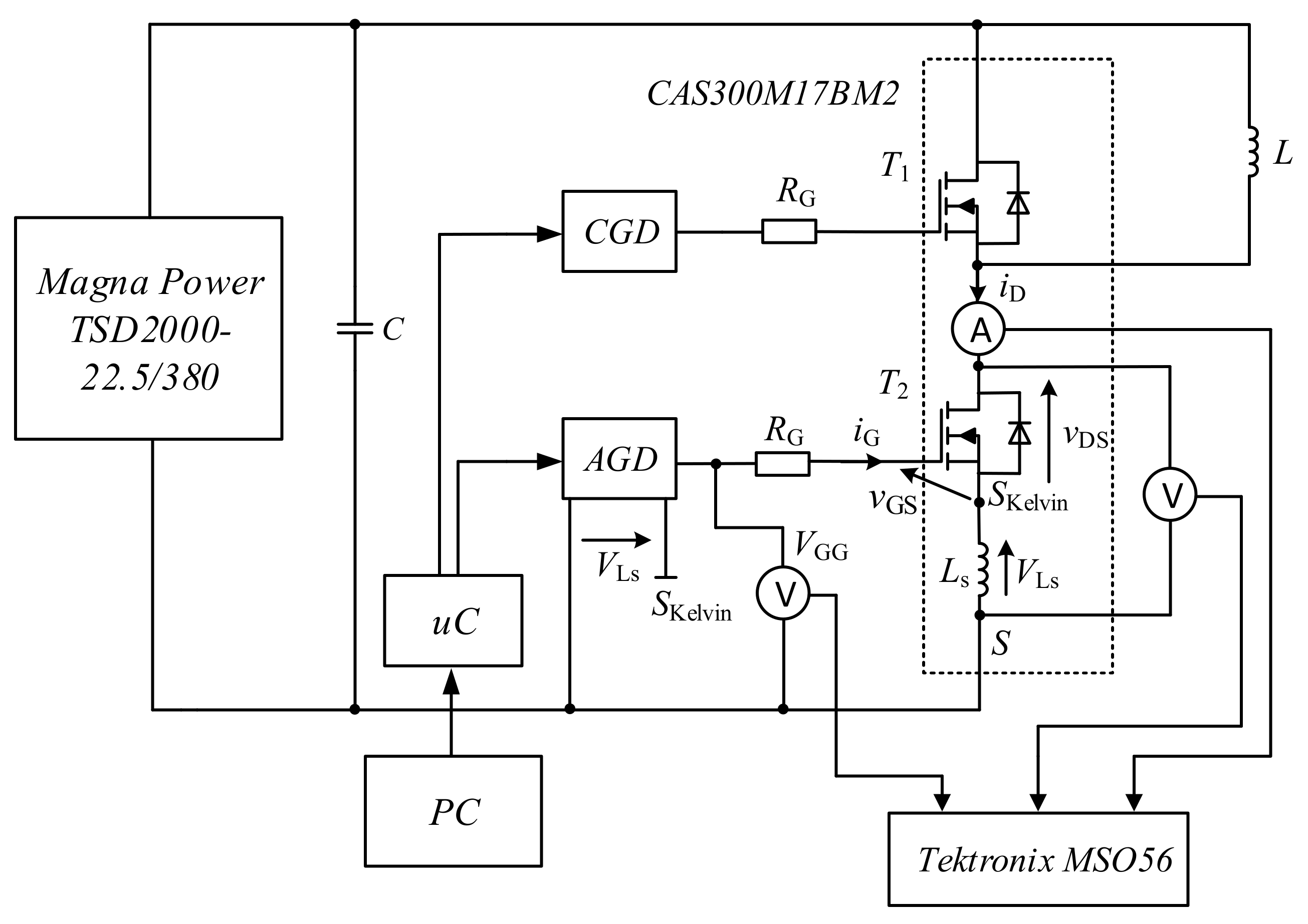
2. The Active Gate Driver

Usually, the AGD input is connected to some feedback signal. A closed-loop signal can be obtained directly from the drain-source voltage, drain current or gate-source voltage [10,11]. However, all of those signals except the gate-source voltage are hard to be measured in case of MV SiC MOSFETs. For example, to measure the vDS voltage, the measuring resistance must be connected between the drain and the source, which makes the complete circuit more complicated and influences the main circuit performance [10]. An approach that is based on the feedback signal in the form of measurement of iD and vDS requires a complex subcircuit to be included in the AGD. In the proposed AGD, the closed loop is provided with the VLs voltage (1). In order to explain this more clearly, a SiC MOSFET connected in the double-pulse test, as presented in Figure 1, is considered. The SiC MOSFET active gate driver is connected to the gate of the transistor through RG and its reference ground is a Kelvin source (SKelvin). SKelvin in SiC MOSFETs is terminal, placed as close as possible to the actual chip inside the module and used for driving purposes. If the device was driven in reference to the power source (S), the source parasitic inductance LS would have undesired effects on the gate current iG. The existence of the parasitic inductance LS between SKelvin and S is naturally caused by internal connections of the SiC MOSFET. Dependence of the temperature for the value of LS is very limited, and it decreases slightly with rising temperature [18]; hence, temperature fluctuations can be omitted when considering this method. From (1), it can be considered that the value of VLs is proportional to the value of LS and diD/dt. Thus, the value of iD and its dynamics can be estimated from VLs. In an ideal case of the turn-on cycle, before iD starts to rise, the VLs value would be always 0 V; at the moment when iD begins to rise, it should have a constant value proportional to the slew rate of iD. After the turn-on cycle, the value of VLs should be 0 V. A feedback loop based on VLs makes the AGD independent from the drain current values during the switching cycle because the drain current dynamic is defined by the changes in the VLs value from 0 V to positive and negative values. Furthermore, VLs peak values are not dependent on the maximal drain current values, but strictly on the diD/dt ratio (1) which is only reliant on the fixed values, thus making it an adequate signal to sense the individual stages of the turn-on cycle. Summarizing, the depicted closed-loop method simplifies the whole structure of the AGD and does not affect the power circuit of the SiC MOSFET.
V Ls = L s d i D t d t

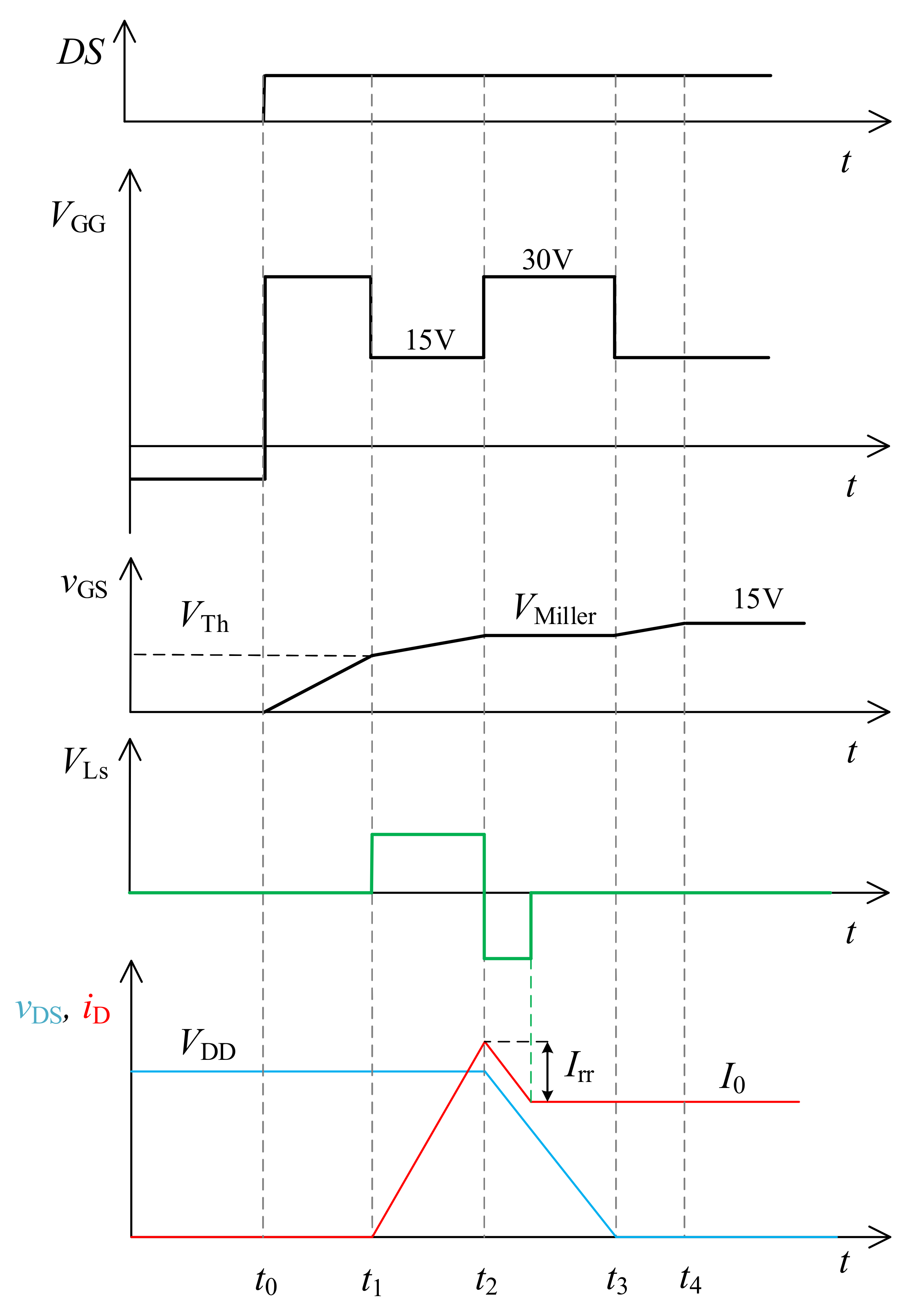
Gate Voltage Manipulation for the Turn-On Cycle Improvment

The measurement of the VLs voltage can be used as a feedback loop for the method presented in Figure 2. The multi-level gate voltage (VGG—see Figure 1) method’s purpose is to decrease power losses, drain current overshoot (Irr) and oscillations of the drain current at the turn-on cycle of a SiC MOSFET by changing the VGG voltage from 15 V to higher at times specified by the regulation system. For the chosen device (CAS300M17BM2 [19]), the VGG value recommended by the manufacturers of SiC MOSFETs is 15 V; thus, such level was chosen. The second level of VGG may be selected between 15 and 30 V—the peak gate voltage allowed for this module; in this case, 30 V was chosen to obtain the maximum increase in the switching speed without damaging the gate oxide layer. Similar to other AGD methods for SiC MOSFET switching improvement, this approach is based on gate current manipulation of the device at the right moments of the switching transient. Thus, in that case, the aim is to improve the turn-on cycle without an unnecessary increase in diD/dt that would cause overshoot and oscillations of the drain current. What distinguishes this method from the many others is that the RG value is constant. Usually, the gate resistor RG is placed as near as possible to the gate terminal of the SiC MOSFET to make the iG path as short as possible. The sequence of the proposed method appears as follows: at t0, the driving signal (DS) is changing from the low state to the high state which begins the turn-on cycle of the SiC MOSFET. The VGG voltage at the same time is changing from −5 (low stage VGG level) to 30 V. The purpose of the first boost of VGG to the value of 30 V is to reduce the time delay between DS and vGS reaching the threshold voltage VTh. At t0, the gate-source voltage vGS starts to rise from zero. After the vGS voltage crosses the threshold voltage VTh at t1, the drain current iD starts to rise. The VLs voltage at t1 will start to rise from 0 V to the value proportional to diD/dt and LS; thus, the beginning of the rise of the current can be sensed. In order to decrease the diD/dt ratio during the interval between t1 and t2, VGG is reduced to 15 V at time t1.
This gate current manipulation stage target is to not cause any serious oscillations of the drain current in the main power circuit. Then, the gate-source voltage is latched from t2 to t3 at Miller’s plateau. t2 is the moment when the drain-source voltage vDS is starting to decrease and when the iD has reached its maximum value, which is sensed based on VLs changes from positive to negative values as the drain current overshoot occurs. The VGG voltage is switched again to 30 V, which increases the dvDS/dt ratio and reduces the period between t2 and t3 which in fact decreases the turn-on power losses in the device and its switching period. Notice that t2 occurs when the drain current has reached its maximum value. In order to suppress further negative effects of iD overshoot, the gate current is increased through modification of the value of VGG to 30 V. To prevent damaging the gate of the device, VGG is again set to 15 V at t3. Finally, at t4, the gate-source voltage vGS reaches 15 V, equal to VGG. The feedback loop of the studied device is based on sensing the two from moments in the turn-on cycle occurring at t1 and t2, based on the VLs measurements and thus responding with changes in the VGG values appropriately, as depicted in Figure 2.
The multi-level gate voltage method impact can be theoretically explained using Equations (2)–(6) based on fundamental knowledge [20]. From Equation (2), it can be concluded that the higher the voltage VGG and the lower the resistance RG, the greater the gate current iG. However, the maximum VGG should be taken into consideration.
i G t = V GG v GS   t R G
In the proposed method, RG is fixed so the gate current is only dependent on the difference between VGG and vGS. The instantaneous gate-source voltage vGS in the switching transient (3) also mainly depends on the VGG, CGD and CGS values. In the proposed method, the VGG voltage is set to 30 V from t0 to t1 to minimize the delay time between the DS signal and the t1 moment where the vGS crosses the threshold value and the drain current starts to rise.
v GS t = V GG 1 e t t 0 τ , τ = R G C GS + C GD
Delay time between t0 when vGS starts to rise and t1 when the MOSFET starts to conduct the drain current that is mainly dependent on the VGG voltage and constant values of the device, as shown in Equation (4). To compensate the delay between the rising edge of the DS signal at t0 and t1 in Δt10, VGG is set to 30 V.
Δ t 10 = t 1 t 0 = τ L n 1 V Th V GG
Another Equation (5) represents the rise time of the drain current from time t1 to t2, where I0 is the drain current in the steady state after the turn-on cycle (see Figure 2), gm is the transconductance and VTh is the threshold voltage at the turn-on cycle. A low value of Δt21 leads to a high diD/dt ratio and, in consequence, current overshoot caused by the Schottky body diode (SBD) and the parasitic elements of the device. Thus, it is the reason for the VGG voltage depletion in t1 from 30 to 15 V.
Δ t 21 = t 2 t 1 = τ L n g m V GG g m V GG V Th I 0
The time of the drain-source voltage falling in the turn-on cycle can be presented by Equation (6), where VDD is the drain-source voltage in the time before t0 and rDS(ON) is the drain-source resistance of the SiC MOSFET. The value of the Δt32 time should be as low as possible in order to increase the dvDS/dt ratio, which will finally decrease the turn-on energy of the MOSFET. Small values of Δt32 do not have any undesirable effects on the switching transient. Therefore, equations show that VGG manipulation based on precise moments in the turn-on cycle can decrease Δt32, which in consequence reduces switching losses. Moreover, the proposed method does not generate drain current overshoot and provides the possibility to increase the switching frequency of the SiC MOSFET only by replacing the gate driver in any SiC MOSFET with a Kelvin source. The SiC MOSFET with an AGD using the multi-level gate voltage technique and feedback loop based on VLs can be switched at same frequency as in normal conditions. To provide an adequate feedback signal, the AGD response time must be shorter than the whole time of the turn-on cycle of the device; thus, the operating frequency of the power device is not constrained. Usually, the maximum switching frequency of an MV SiC MOSFET power module is limited by the thermal dependency of the device on power losses. In the case of a transistor in power modules, the switching frequency is much lower (100–500 times) than the sum frequency of the turn-on and turn-off cycles.
Δ t 32 = t 3 t 2 = R G C GD V DD I 0 r DS ON V GG V Th

3. Simulation Study

The proposed AGD circuit in the DPT configuration is presented in Figure 3. The chosen device is a half-bridge module (CAS300M17BM2), so the AGD is controlling only transistor T2 (see Figure 3) during the DPT. T2’s gate current iG is actively controlled by the AGD with the previously described method and T1’s gate is connected constantly to −5 V (in reference to its source). In this particular case, LS is equal to 15 nH based on the datasheet.
Simulation verification of the proposed AGD multi-level gate voltage method based on the parasitic inductance voltage measurement was conducted in Saber RD software. The CAS300M17BM2 module simulation model was provided by the producer of the device. The first steps of the research were to observe the waveforms of VLs with CGD and, basing on this, conclude if the method can be used in all SiC MOSFETs. The purpose of the simulation study was to verify the assumptions about the decrease in the turn-on time and energy in the chosen method. Finally, the main aim of the simulation was to measure power losses of the CGD at the turn-on cycle and compare them with the AGD. In simulations, the SiC MOSFET half-bridge module was connected in the DPT setup (Figure 3). Transistor T1 was turned off and T2 was the DUT. The gate resistance RG of both the AGD and CGD was set to a fixed value of 20 Ω. The main assumption of the similar value of the RG in tests of the AGD and CGD was to obtain the same diD/dt ratio at the turn-on of the device for both cases. T1 was connected in parallel to the inductor L = 110 µH. The CGD gate voltage VGG was fixed at a value of 15 V at the turn-on (according to datasheet recommendations). The AGD gate voltage VGG (Figure 2) had a variable value of either 15 or 30 V. The AGD simulation was conducted using the feedback signal from VLs, which was connected to the Saber RD logical and electrical elements to provide the active control of the VGG voltage. Delays of the components were not considered in that stage of the research. The DPT was conducted for four operating conditions at the turn-on cycle for the VDD voltages of 700 or 900 V and I0 currents of 170 or 270 A. However, the observations of the response of the AGD on the increasing I0 current had smaller step of change to verify that this solution is independent from the variation in the drain current. The turn-on cycle using the CGD for VDD = 700 V, I0 =270 A is shown in Figure 4. In comparison, the turn-on cycle with the AGD for the very same conditions is shown in Figure 5, where the difference in the voltage falling time is visible. The vds/dt ratio increased without any serious oscillations of iD, thus shortening the turn-on cycle of the device. Notice that in Figure 4 and Figure 5, the iD rising time is marked, and in both simulated cases, the diD/dt ratio was the same (1 kA/µs) due to identical RG values and VGG levels in Δt21 (see Figure 2). Additionally, the simulations show that the AGD compensates the delay between the rising of the vGS voltage and the moment when the device starts to conduct the drain current.
Table 1 presents the results of the previously mentioned simulation. The turn-on energy mostly decreased for VDD = 900 V, I0 = 270 A. The turn-on energy settled at 65.5 mJ for the CGD, whereas for the AGD, it reached just 45.9 mJ, resulting in a difference of roughly 30%. The smallest percentage disparity was measured for VDD = 900 V, I0 = 170 A, and it was equal to 15%.
Simulations of the AGD in Saber RD software confirmed that the multi-level VGG method is able to decrease the turn-on energy of the transistor from the CAS300M17BM2 SiC MOSFET module, and there is the possibility to use the feedback signal from the VLs voltage measurement, thus confirming the presumptions.

4. Experimental Verification

After the simulation study, the proposed AGD was verified by means of experiments—the simplified main electrical circuit of the proposed AGD for the MV SiC MOSFET is presented in Figure 6. After the simulation research and datasheet-based calculations, it was concluded that the VLs voltage will be in the operational range of the integrated electronical circuits (0/5 V) after adequate signal conditioning. The AGD feedback loop is provided by the connection of the filtering circuit of the AGD to the power source S of the DUT. All depicted voltage levels in Figure 6 are referenced to the potential of the Kelvin source SKelvin. During the short switching time of the chosen SiC MOSFET with high-level power turn-on conditions, VLs is filtered by ferrite beads (FBD) from high-frequency noises to prevent damaging the vulnerable logical gates. The filtered signal is then delivered to the operational amplifiers circuit. In this particular case, two LM-7171 high-speed operational amplifiers were used in the differential configuration. The purpose of this stage is to separate the measuring signal into two independent measuring paths and to add the offset to both of them. Two measurement paths are the reason to have independent signal loops for sensing t1 and t2 (see Figure 2).
The outputs of the amplifiers are connected to low-propagation delay comparators, TLV3501 (4.5 ns), with the reference voltages Vref1 and Vref2. Values of Vref1 and Vref2 were obtained based on the datasheet of the device (switching speeds and LS = 15 nH). Note that these parameters may differ and the driver applied for different modules may need additional tuning. For the considered CAS300M17BM2, approximate maximum and minimum values of VLs should be in the range ±7.8 V for RG = 20 Ω. However, this value is too high to be provided for the TLV3501 comparators (0/5 V). Operational amplifiers suppressed this voltage and added offset, meaning that their output signals have maximum values of 5 V and minimum values of 0 V. It means that in steady state, where the device is not switching, the outputs of the amplifiers are 2.5 V. Thus, Vref1 has a value of 2.5 V + 10% of 2.5 V, which is 2.75 V, and its role is to identify when iD starts to rise during the turn-on cycle. The 10% tolerance secures it from any inappropriate disturbances that could cause switching of the comparator due to the parasitic in the device. On other hand, the Vref2 role is to sense moment t2 (see Figure 2). The value of this reference voltage was set to 4 V after approximated calculations of the expected VLs value. t2 is sensed based on the change in the operational amplifier output from a value above 2.5 to below 2.5 V, which corresponds to the VLs change from positive to negative voltages. Comparators are responsible for sensing the t1 and t2 time moments (see Figure 2) of the VGG voltage modification. Thus, one of the comparators detects the drain current rising moment t1 which corresponds to VGG depletion from 30 to 15 V. The role of the second comparator is to sense when iD starts to fall, which is caused by the overshoot of current iD at t2 and it is responsible for the VGG increase from 15 to 30 V. Since voltage VLs represents the dynamics of the drain current Vref1 and Vref2 can be set to persistent values, the comparator answering to sense the t2 role is not to define the exact value of VLs, but rather to sense the moment when diD/dt begins to reach a negative value (see Figure 2). Subsequently, the signal is provided to the logical gate circuit and then connected to an X4340 high-speed driver. The logical subcircuit is based on high-speed logical gates, which are responsible for detecting the rising edge of the comparators’ outputs and for protecting the VGG switching sequence. The purpose of that is so that VGG would not set inappropriate values at unsuitable moments of the turn-on cycle. It is shown as a block to make the diagram more simplified and clearer. X4340 handles switching the voltage from 15 to 30 V dependently on the logical signal on its input with a low propagation delay. Voltage levels 15/−5 V are supplied by isolated DC/DC converters, MGJD241505. The supply voltage of 30 V is provided from the boost DC/DC converter TP61175. The last part of the circuit is the IXDN630 current amplifier whose role is to turn on or turn off the device according to the value of the DS signal. The gate resistance RG of the AGD was constant and equal to 20 Ω. Summary propagation delays of the used components were calculated from the data provided from the manufacturers. The response times of the AGD were under consideration during the design stage of the research, in correspondence with the turn-on time of the studied SiC MOSFET. Even with the low switching period of the chosen device components, the AGD operated properly.
A photo of the designed AGD with the detailed marks of its visible components is shown in Figure 7. The AGD was optically isolated from the logical signal DS using HFBR-2531 optical receivers. As it can be noticed, the AGD consists of two connected PCBs (Printed Circuit Boards). The role of the first two-layer PCB (blue) is to provide a power supply to all integrated circuits of the device, switch the voltage from 15 to 30 V and amplify the logical signal DS. The second subcircuit of the AGD is a four-layer PCB (black), and it is directly connected to the power source of the T2 MOSFET. Filtering, conditioning and logical circuits were placed onto this board of the AGD. The main purpose of that was to suppress any disturbances in the VLs measurements.
The experimental setup with a half-bridge module (CAS300M17BM2) and a suitable inductor (L = 110 µH) connected in the DPT circuit is presented in Figure 8. Both the CGD and AGD were controlled by a microcontroller (uC) unit. Measurements were made using a Tektronix MSO56 scope with differential medium-voltage probes (P5205A) with a measurement tolerance of ±2% and a Rogowski coil (CWTMini HF3B) with a tolerance of ±2%. Delay times of the probes were calculated from the datasheets and were further included in the measurements to provide correct results. The AGD and CGD were compared in the same experimental conditions. Thus, the tolerances of the used probes can be omitted when both devices are compared. The drain current iD, drain-source voltage vDS and positive bus of the VGG voltage were measured. A 2 kV DC power supply was provided by a Magna Power TSD 2000-22.5/380 with the output connected in parallel to the energy storage (C = 150 µF). Next, Figure 9 presents the photo of the experimental setup in the DPT configuration during experiments.
The first test was conducted with the CGD—Figure 10 (VDD = 700 V, I0 = 270 A) presents the turn-on cycle for a standard gate voltage of VGG = 15 V. After the drain current overshoot, continuous, weakly damped oscillations can be observed, and they are continued after the end of the turn-on process where the impact on the drain-source voltage is also visible. The voltage fall time is slightly above 300 ns. Comparing it to the same turn-on cycle from Figure 11, the impact of the AGD on iD and vDS can be noticed. As expected, the AGD increased the speed of the vDS voltage decrease (<200 ns) and shortened the cycle without causing any negative effects on the transient. Individual influences of the AGD on the diD/dt and dvDS/dt ratios and drain current oscillations are marked on the waveforms presented in the following Figure 12 (VDD = 900 V, I0 = 270 A). The shown voltage VGG+ is the positive rail of the gate driver and, as it can be seen, the switching from a value of 15 to 30 V was obtained in proper moments of the cycle. The first decrease in the VGG voltage was delayed on purpose to increase the diD/dt ratio which occurs in the turn-on energy depletion without iD overshoot in crucial moments. The AGD had the most visible impact on the dvDS/dt ratio, decreasing ipso facto the falling time of vDS. Moreover, the AGD delay between the ideal point of the switching VGG+ voltage can be noticed in Figure 12. In addition, the response time of the AGD can be noticed, which is visible as a result of the summary delays of used electronical components and filtering subcircuits. Comparing both obtained waveforms for the AGD, the damping of the drain current oscillations is greater in the case with VDD = 900 V, contrary to the case with VDD = 700 V. However, in both shown AGD cases, the impact on the drain current oscillations can be seen.
In summary, the experimental measurements of the turn-on energy Eon of the AGD and CGD in the same switching conditions (VDD, I0 and probes’ tolerances) are shown in Table 2. The turn-on energy of the CAS300M17BM2 MV SiC MOSFET using the AGD was decreased in all of the measured conditions compared to the CGD. The turn-on energy was decreased even by 10.1%, with an average of 7% for all measured turn-on energies. Comparisons of the obtained results from experimental and simulation studies are presented in Figure 13.

5. Conclusions

In this paper, an AGD for a 1.7 kV/325A SiC MOSFET power module was proposed and validated via simulations and experiments. A mix of multi-level gate voltage and proper measurements of the voltage across the parasitic source inductance proved a positive impact on the turn-on process of the transistor. The AGD was able to deplete the turn-on energy of the power SiC MOSFET by 7% on average and shorten the turn-on cycle without interference in the main circuit. Furthermore, experimental validation showed a higher dvds/dt rate and, subsequently, measurements confirmed that the chosen method has no negative effect on the drain current oscillations and even suppresses them. Moreover, the device shown in this paper was designed based on off-the-shelf integrated circuits, which makes it a low-cost solution. Additionally, due to use of an integrated boost converter, the AGD needs only one level of the positive supply voltage (15 V) which leads it to be less complex in terms of structure. Finally, the proposed driver can also be used in other models of MV SiC MOSFETs where the Kelvin source and the power source of the device are provided. Further research in the case of turn-off cycle improvement with the shown methods is under consideration.

Author Contributions

Main concept, J.R.; simulation study, B.L.; formal analysis and hardware validation B.L., P.T. and R.K.; writing B.L.; review and editing, P.T., J.R. and R.K.; project administration and funding acquisition J.R. All authors have read and agreed to the published version of the manuscript.

Funding

This research was funded by National Science Center, Poland project no. 2017/27/B/ST7/00970.

Data Availability Statement

The data presented in this study are available on request from the corresponding author. The data are not publicly available due to further research plans of the improved device discussed in that paper.

Conflicts of Interest

The authors declare no conflict of interest.

References

  1. Mishra, P.; Maheshwari, R. Evaluation of All SiC MOSFET Based Voltage Source Inverter with Open Loop Induction Motor. In Proceedings of the 2017 14th IEEE India Council International Conference (INDICON), Roorkee, India, 15–17 December 2017; pp. 1–6. [Google Scholar]
  2. Sayed, H.; Surf, A.; Zhang, J. Investigation of the effects of load parasitic inductance on SC MOSFETs switching performance. In Proceedings of the 2017 IEEE International Conference on Industrial Technology (ICIT), Toronto, ON, Canada, 22–25 March 2017; pp. 125–129. [Google Scholar]
  3. Nayak, P.; Hague, K. Modeling of switching behavior of 1200 V sick MOSFET in presence of layout parasitic inductance. In Proceedings of the 2016 IEEE International Conference on Power Electronics, Drives and Energy Systems (PEDES), Trivandrum, India, 14–17 December 2016; pp. 1–6. [Google Scholar]
  4. Sugihara, Y.; Nanamori, K.; Ishiwaki, S.; Hayashi, Y.; Aikawa, K.; Umetani, K.; Hiraki, E.; Yamamoto, M. Analytical investigation on design to avoid oscillatory false triggering of fast switching SiC-MOSFETs. In Proceedings of the 2017 IEEE Energy Conversion Congress and Exposition (ECCE), Cincinnati, OH, USA, 1–5 October 2017; pp. 5113–5118. [Google Scholar]
  5. Dalal, D.N.; Christensen, N.; Jørgensen, A.B.; Jørgensen, J.K.; Bęczkowski, S.; Munk-Nielsen, S.; Uhrenfeldt, C. Impact of Power Module Parasitic Capacitances on Medium-Voltage SiC MOSFETs Switching Transients. IEEE J. Emerg. Sel. Top. Power Instr. Electron. 2020, 8, 298–310. [Google Scholar] [CrossRef]
  6. Rasoanarivo, I.; Dell’Isola, D. Improvements of switching energy of SiC transistor with respect of chip integrity and EMC standards. In Proceedings of the 2017 19th European Conference on Power Electronics and Applications (EPE’17 ECCE Europe), Warsaw, Poland, 11–14 September 2017; pp. P.1–P.10. [Google Scholar]
  7. Kim, T.; Feng, D.; Jang, M.; Agelidis, V.G. Common Mode Noise Analysis for Cascaded Boost Converter with Silicon Carbide Devices. IEEE Trans. Power Electron. 2017, 32, 1917–1926. [Google Scholar] [CrossRef]
  8. Han, Y.; Lu, H.; Li, Y.; Chai, J. Open-Loop Gate Control for Optimizing the Turn-ON Transition of SiC MOSFETs. IEEE J. Emerg. Sel. Top. Power Electron. 2019, 7, 1126–1136. [Google Scholar] [CrossRef]
  9. Li, H.; Jiang, Y.; Feng, C.; Yang, Z. A Voltage-injected Active Gate Driver for Improving the Dynamic Performance of SiC MOSFET. In Proceedings of the 2019 IEEE Energy Conversion Congress and Exposition (ECCE), Baltimore, MD, USA, 29 September–3 October 2019; pp. 6943–6948. [Google Scholar]
  10. Paredes, A.; Fernandez, E.; Sala, V.; Ghorbani, H.; Romeral, L. Switching trajectory improvement of SiC MOSFET devices using a feedback gate driver. In Proceedings of the 2018 IEEE International Conference on Industrial Technology (ICIT), Lyon, France, 19–22 February 2018; pp. 847–852. [Google Scholar]
  11. Nayak, P.; Hatua, K. Active gate driving technique for a 1200 V SiC MOSFET to minimize detrimental effects of parasitic inductance in the converter layout. In Proceedings of the 2016 IEEE Energy Conversion Congress and Exposition (ECCE), Milwaukee, WI, USA, 18–22 September 2016; pp. 1–8. [Google Scholar]
  12. Wang, J.; Shen, Z.; DiMarino, C.; Burgos, R.; Boroyevich, D. Gate driver design for 1.7 kV SiC MOSFET module with Rogowski current sensor for shortcircuit protection. In Proceedings of the 2016 IEEE Applied Power Electronics Conference and Exposition (APEC), Long Beach, CA, USA, 20–24 March 2016; pp. 516–523. [Google Scholar]
  13. Marzoughi, A.; Burgos, R.; Boroyevich, D. Active Gate-Driver with dv/dt Controller for Dynamic Voltage Balancing in Series-Connected SiC MOSFETs. IEEE Trans. Ind. Electron. 2019, 66, 2488–2498. [Google Scholar] [CrossRef]
  14. Krishna, M.V.; Hatua, K. Closed loop analog active gate driver for fast switching and active damping of SiC MOSFET. In Proceedings of the 2018 IEEE Applied Power Electronics Conference and Exposition (APEC), San Antonio, TX, USA, 4–8 March 2018; pp. 3017–3021. [Google Scholar]
  15. Yang, Y.; Wen, Y.; Gao, Y. A Novel Active Gate Driver for Improving Switching Performance of High-Power SiC MOSFET Modules. IEEE Trans. Power Electron. 2019, 34, 7775–7787. [Google Scholar] [CrossRef]
  16. Sobieski, R.; Trochimiuk, P.; Skoneczny, H.; Rąbkowski, J. Impact of a gate drive on performance of three-phase inverters based on 3.3 kV SiC MOSFETs. In Proceedings of the 2020 Progress in Applied Electrical Engineering (PAEE), Koscielisko, Poland, 21–26 June 2020; pp. 1–7. [Google Scholar]
  17. Li, X.; Zhang, L.; Guo, S.; Lei, Y.; Huang, A.Q.; Zhang, B. Understanding switching losses in SiC MOSFET: Toward lossless switching. In Proceedings of the 2015 IEEE 3rd Workshop on Wide Bandgap Power Devices and Applications (WiPDA), Blacksburg, VA, USA, 2–4 November 2015; pp. 257–262. [Google Scholar]
  18. Zeng, Y.; Yi, Y.; Liu, P. An Improved Investigation into the Effects of the Temperature-Dependent Parasitic Elements on the Losses of SiC MOSFETs. Appl. Sci. 2020, 10, 7192. [Google Scholar] [CrossRef]
  19. Wolfspeed CAS300M17BM2 Datasheet. Available online: https://www.wolfspeed.com/downloads/dl/file/id/185/product/102/cas300m17bm2.pdf (accessed on 2 March 2021).
  20. Rashid, M.H. Power Electronics Handbook, 1st ed.; Academic Press: San Diego, CA, USA, 2001; pp. 86–88. [Google Scholar]
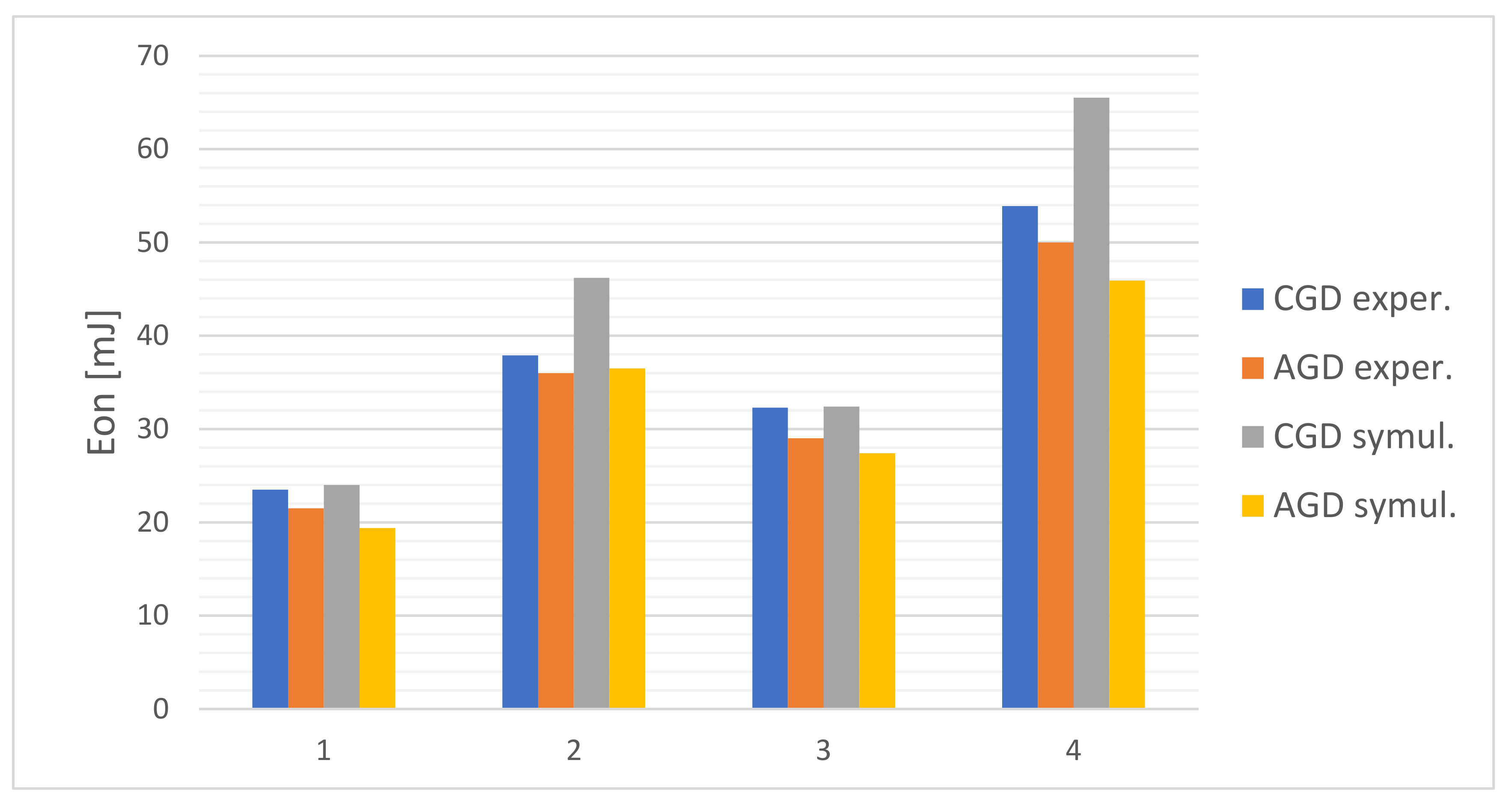
Figure 1. SiC MOSFET (DUT) in the double-pulse test (DPT) setup with the active gate driver (AGD) in which the feedback loop is based on the parasitic source inductance voltage (VLs). VGG—gate voltage, RG—gate resistance, SKelvin—Kevin source, iD—drain current, vDS—drain-source voltage, LS—parasitic inductance, vGS—gate-source voltage.
Applsci 11 02210 g001
Figure 2. The multi-level gate voltage method waveforms for the turn-on cycle improvement of the SiC MOSFET with an inductive load. DS—logical driving signal of the device, VGG—gate voltage of the SiC MOSFET, vGS—gate-source voltage, vDS—drain-source voltage, iD—drain current, VDD—drain-source voltage before the turn-on of the MOSFET, I0—drain current after switching on the device, VTh—threshold voltage, VMiller—Miller voltage, Irr—drain current overshoot, VLs—ideal source parasitic inductance voltage waveform.
Applsci 11 02210 g002
Figure 3. The AGD in DPT setup with half-bridge module 1.7 kV/325 A SiC MOSFET CAS300M17BM2.
Applsci 11 02210 g003
Figure 4. The turn-on cycle of the SiC MOSFET from module CAS300M17BM2 using conventional gate driver (CGD). VDD = 700 V, I0 = 270 A, VGG = 15 V.
Applsci 11 02210 g004
Figure 5. The turn-on cycle of the SiC MOSFET from module CAS300M17BM2 using AGD. VDD = 700 V, I0 = 270 A.
Applsci 11 02210 g005
Figure 6. Simplified diagram of the AGD.
Applsci 11 02210 g006
Figure 7. Photo of the designed AGD. 1—filtering and logical signal board (AGD input), 2—DC/DC boost converter 15/30 V, 3—isolated power supply, 4—optical receivers HFBR 2531-Z, 5—output of the AGD.
Applsci 11 02210 g007
Figure 8. Experimental setup of the DPT with a medium-voltage (MV) SiC MOSFET CAS300M17BM2 module.
Applsci 11 02210 g008
Figure 9. Photo of the experimental setup. 1—CAS300M17BM2 module, 2—DC bus and blocking capacitors.
Applsci 11 02210 g009
Figure 10. The turn-on cycle of the SiC MOSFET from module CAS300M17BM2 with CGD. VDD = 700 V, I0 = 270 A.
Applsci 11 02210 g010
Figure 11. The turn-on cycle of the SiC MOSFET from module CAS300M17BM2 with AGD. VDD = 700 V, I0 = 270 A.
Applsci 11 02210 g011
Figure 12. The turn-on cycle of the SiC MOSFET from module CAS300M17BM2 using AGD with the VGG+ voltage waveform. VDD = 900 V, I0 = 270 A.
Applsci 11 02210 g012
Figure 13. Chart of the turn-on energy for CGD and AGD both in experimental and simulation conditions. 1—VDD = 700 V, I0 = 170 A, 2—VDD = 700 V, I0 = 270 A, 3—VDD = 900 V, I0 = 170 A, and 4—VDD = 900 V, I0 = 270 A.
Applsci 11 02210 g013
Table 1. The turn-on energy losses of CGD and AGD comparison from the simulation study.
VDDI0Eon CGDEon AGD
700 V170 A24.0 mJ19.4 mJ
700 V270 A46.2 mJ36.5 mJ
900 V170 A32.4 mJ27.4 mJ
900 V270 A65.5 mJ45.9 mJ
Table 2. The turn-on energy losses of AGD and CGD comparisons from the experimental test.
VDDI0Eon CGDEon AGD
700 (±14) V170 (±3.4) A23.5 (±0.94) mJ21.5 (±0.86) mJ
700 (±14) V270 (±5.4) A37.9 (±1.52) mJ36.0 (±1.44) mJ
900 (±18) V170 (±3.4) A32.3 (±1.29) mJ29.0 (±1.16) mJ
900 (±18) V270 (±5.4) A53.9 (±2.16) mJ50.0 (±2.0) mJ
Publisher’s Note: MDPI stays neutral with regard to jurisdictional claims in published maps and institutional affiliations.

