Article

Metal-Organic Hybrid Metamaterials for Spectral-Band Selective Active Terahertz Modulators

1
S. LSI Metrology & Inspection, Samsung Electronics, Yongin 17113, Korea
2
Department of Physics and Optoelectronics Convergence Research Center, Chonnam National University, Gwangju 61186, Korea
3
Department of Physics and Department of Energy Systems Research, Ajou University, Suwon 16499, Korea
4
Advanced Photonics Research Institute, GIST, Gwangju 61005, Korea
*
Author to whom correspondence should be addressed.
Appl. Sci. 2021, 11(6), 2765; https://doi.org/10.3390/app11062765
Submission received: 3 March 2021 / Revised: 17 March 2021 / Accepted: 17 March 2021 / Published: 19 March 2021
(This article belongs to the Special Issue Advances of THz Spectroscopy)

Abstract

:
Optically controlled spectral-band selective terahertz (THz) modulators based on metal-organic hybrid metamaterials were investigated. An artificially structured material, which consists of two single split-ring resonators put together on the split gap side, was patterned on a silicon substrate to generate frequency-selective properties. An active layer of an organic thin film (fullerene derivative [6,6]-phenyl-C61-butyric acid methyl ester, also called PCBM) was deposited on the metamaterial-silicon structure for modulating the transmission of incident THz radiation. The metal-organic hybrid metamaterials enabled active control of spectral bands present in the transmission spectra of THz waves. In addition, the changes in the photo-excited carrier density due to the transfer of charges between the layers were quantitatively analyzed by simulation results.

1. Introduction

Terahertz (THz) wave technologies have attracted much attention for their useful application in various fields, such as high-speed wireless communication, spectroscopy, and sensing/imaging systems [1,2,3,4,5]. In particular, the realization of active THz devices is necessary for improved functionalities of spectroscopy and imaging systems and advancement in next-generation wireless communications. By utilizing various materials or structures, such as semiconductor nanostructures, graphene, vanadium dioxide, plasmonic structures, and metamaterials, several studies have demonstrated possibilities of active modulation of transmission, reflection, spatial position, polarization, and phase of THz waves [6,7,8,9,10,11].
Recently, active THz modulation based on organic-based hybrid structures has been suggested for realizing an active control of the transmission of THz waves [12,13]. The change in photo-induced carrier densities, caused by the dynamics of photo-excited carriers in the hybrid structures, renders control of the amount of transmission of incident THz waves possible. This method is receiving special attention owing to its various advantages, such as high modulation efficiency, extreme broadband modulation, and excellent compatibility with existing silicon-based technologies. Our group reported organic-based active THz modulators with almost 100% modulation efficiency [14]. Several other research groups have reported active THz modulators with high modulation efficiencies by utilizing various structures based on organics, polymers, and perovskites [15,16,17,18].
More recently, artificially crafted composite materials (known as metamaterials) combined with the organic-based hybrid structures presented above have been proposed to realize active tuning of the resonant response, which enables frequency-selective filtering or spectral-band engineering [19,20,21,22,23,24,25,26]. In particular, active THz filters based on metamaterial units of split-ring resonators (SRRs) offer wide variability in terms of structural dimensions for dipole and LC resonances. Moreover, while maintaining high modulation efficiency and actively controllable features of the THz waves, which are realized by an organic material-based hybrid structure, it is necessary to create THz modulators with the functions of frequency-selective filtering or spectral-band engineering.
In this paper, we demonstrated optically controllable, spectral-band selective THz modulators, still having the property of high modulation efficiency, based on silicon-metamaterial-organic hybrid structures. The metamaterial units, which consisted of two single SRRs put together on the split gap side, fabricated on a Si substrate, exhibited frequency-selective properties over multiple spectral bands. The organic thin film, fullerene-derivative [6,6]-phenyl-C61-butyric acid methyl ester (also called PCBM), deposited on the metamaterial-Si structure acted as an active layer for modulating the transmission of incident THz radiation. By combining the organic thin film with the metamaterial-Si structure, an active control of the spectral bands present in the transmission spectra of THz waves was achieved. Furthermore, the simulations obtained to match the experimental results, by fine-tuning of the electrical conductivity values of the PCBM and Si layers, aided the understanding of the underlying mechanisms of the phenomenon, as well as estimated the amount of change in photo-induced carrier density in the tri-layer structure.

2. Methods

As shown in Figure 1a, the metamaterial units, which consist of a planar array of SRR elements, were fabricated on a Si substrate with a high resistivity of up to 1.0 × 10⁵ Ω·cm by a conventional photolithographic technique. The unit elements were arranged with periods of Px = 100 μm and Py = 100 μm. A single unit cell of the metamaterial structure, shown in Figure 1b, had a 100-nm-thick metallic layer (2 nm Cr adhesive layer and ~100 nm Au film), 4 μm line width, outer dimensions of dx = dy = 74 μm, and split gap spacing of g = 4 μm. The SRR was a suitable structure to independently control the two resonance modes, fundamental LC resonance and dipolar resonance, by adjusting the polarization of incident THz waves.
As shown in Figure 1c, an organic thin layer of PCBM molecules (>99.5%), purchased from Sigma-Aldrich (product number: 684449), was deposited on the metamaterial/Si hybrid structure using a spin coating method. By controlling the organic concentration and the rotation speed range of a spin coater, a PCBM thin layer with a thickness of approximately 200 nm was fabricated. To improve the modulation efficiency, the thermal annealing process of the fabricated samples was carried out on a hot plate at temperatures above 200 °C for 1 h. The dynamics of photo-excited carriers, especially at the interface between the PCBM and Si substrate, considerably depended on the relationship between the highest occupied molecular orbital (HOMO) and lowest unoccupied molecular orbital (LUMO) energy levels shown in Figure 1d. According to the energy level diagram, the photo-excited electrons in the Si substrate were injected into the PCBM layer, and the photo-excited holes diffused within the Si layer.
The transmission through the samples was measured by a THz time-domain spectroscopy (THz-TDS) system. Pulsed THz waves were generated by a p-type InAs crystal mainly due to an anisotropic photocurrent in the surface electric field and were detected by a photoconductive antenna method [27,28,29]. As shown in Figure 1e, the THz waves were incidented onto the surface area of the samples restricted by a 3-mm-diameter pinhole, while the optical beam from a cw diode laser with a center wavelength of 785 nm was incidented at an angle of 45° on the same area. The transmitted time-domain signals were measured under the conditions of both with and without photoexcitation, and the transmission amplitude spectra were obtained by carrying out a fast Fourier-transform method. Here, the THz transmission measurements were conducted by changing the power of the incident optical beam.
Numerical simulations were performed by finite element modeling using the COMSOL Multiphysics software. Accurate simulation results could be obtained based on an incident plane wave of THz radiation using the COMSOL wave optics module. Owing to the periodic nature of the metamaterial elements, relatively easier simulations were possible because they could be performed in a unit cell, shown in Figure 1b, with periodic boundary conditions. To quantitatively understand the carrier dynamics in the PCBM/metamaterial/Si hybrid structures, the simulations, which were conducted to efficiently match the experimental results, were performed for different values of electric conductivity of the PCBM and Si layers.

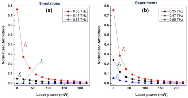
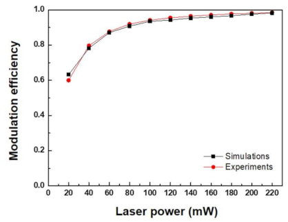
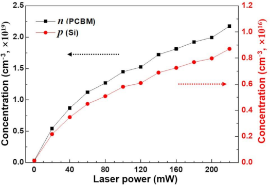
3. Results and Discussion

Figure 2a shows the simulation results of the transmission amplitude spectrum of the metamaterials using the COMSOL Multiphysics software. The simulations show two obvious transmission dips located at the frequencies of 0.35 THz and 0.85 THz. To obtain the simulation results, the electric-conductivity values that corresponded well to the experimental results, shown in Figure 2b, were selected. The transmission amplitude spectra of the PCBM/metamaterial/Si hybrid structure, as shown in Figure 2b, were measured by varying the laser power of the optical beam for photoexcitation. The polarization of the incident THz waves was parallel to the metal lines present in the center of the unit structure. Similar to the simulations, the experimental results also showed two obvious transmission dips, located at the frequencies of 0.35 THz and 0.85 THz, with the exception that the dip values at both the frequencies were slightly different.
As shown in Figure 2a,b, the transmission rapidly decreased as the laser power of the optical beam increased over the entire THz-frequency ranges. As the laser power of the optical beam for photoexcitation increased, the concentrations of both photo-excited electrons and holes increased, and subsequently, the electric conductivity of the silicon substrate and the PCBM thin layer increased steadily. This phenomenon was caused by efficient charge separation owing to the photo-induced electron transfer from the excited states of the Si substrate into the PCBM layer, changing the tri-layer hybrid structures from insulating to metallic [13].
The measured transmission spectra showed two obvious resonant dips located at 0.35 THz and 0.85 THz, as shown in Figure 2b. According to the electric-field distribution, as shown in the left inset of Figure 2b, the transmission dip located at 0.35 THz may have been due to a fundamental inductive–capacitive (LC) resonance mode, since the electric field was concentrated in the small volume near the gaps at the center of the metamaterial units, and the circular current flow appeared on the metallic ring (not shown here). In addition, the second-order LC resonance mode, which is similar to the horizontal electric quadrupole mode, appeared at a frequency of 0.85 THz. Furthermore, the transmission of the spectral band located between the two resonance frequencies could be manipulated by varying the amount of photoexcitation. In principle, the range of spectral bands to be transmitted can be engineered by manipulating the structures and dimensions of metamaterials.
Figure 3 shows the intensity values obtained from the simulations (Figure 3a) and the experimental results (Figure 3b) at the two resonant frequencies of f1 = 0.35 THz and f2 = 0.85 THz and, in addition, at the peak frequency (f3 = 0.47 THz) of the spectral band located between the two resonant frequencies. Unlike the two frequencies at resonance, the peak frequency of the spectral band was dramatically varied with increasing the laser power of optical beam. This means that the hybrid structures of organic/metamaterial/semiconductor could be a promising structure for realizing actively controllable band-pass filters or spectral-band engineering.
It is important to compare the experimental and simulated values of spectral intensity modulation efficiency that is defined as
M = | E u n ( ω ) | 2 d ω | E e x ( ω ) | 2 d ω | E u n ( ω ) | 2 d ω ,
where Eex and Eun represent the electric-field amplitude spectra measured with and without photoexcitation, respectively [22]. Figure 4 shows the spectral intensity-modulation efficiency plotted as a function of the laser power of the optical beam. The black squares and red circles indicate the values extracted from the simulations and experimental results, respectively.
The most important variables required for simulations, the electrical conductivities of electrons and holes, were selected so that the derived simulation results matched the experimental results well. Furthermore, the electrical conductivity was proportional to the product of the carrier concentration and mobility. If a material has both electrons and holes, the total electrical conductivity is given by
σ = e ( n μ e + p μ h )
where e, μe, μh, n, and p indicate the elementary charge, carrier mobility of electrons, carrier mobility of holes, carrier concentration of electrons, and carrier concentration of holes, respectively.
Figure 5 shows the carrier concentrations of electrons in the PCBM layer and holes in the Si substrate, calculated using the above formula as well as from the simulation results. Here, the hole drift mobility in high-resistivity silicon with a bulk resistivity of more than 105 Ω·cm was 500 cm2/(V·s), and the electron mobility in a thin film of PCBM molecules thermally annealed at 150 °C was approximately 2.0 × 10⁻⁴ cm2/(V·s) [30]. The values of electrical conductivity selected to perform simulations to realize the experimental results are listed in Table 1 below. Using the values of the electrical conductivity and carrier mobility, the carrier concentrations of electrons in the PCBM thin film and holes in the Si substrate are calculated as shown in Figure 5.
Considering the excess carrier distribution generated by an optical beam under the continuous photoexcitation by a cw optical laser, the excess carrier concentration gradient over all depths in both the PCBM and silicon layers was not found to be significantly large in a dynamic equilibrium. The carrier concentrations could, therefore, be considered uniform throughout the sample. Spatially separated electrons and holes at the PCBM-Si interface allow sustained maintenance of a relatively high carrier concentration while rendering both the layers sufficiently metallic in the THz frequency region.
The carrier concentration values shown in Figure 5 fully demonstrate that the metalized structures effectively blocked the incident THz waves. This procedure, using measured THz time-domain signals and their corresponding simulations, could be utilized further to study the properties of photo-induced charge carriers, such as carrier concentration and electrical conductivity, even in the organic/metamaterial/semiconductor hybrid structures. Therefore, we infer that the organic-metamaterial-based hybrid structures are useful in designing actively controllable multifunctional THz filters, and THz technologies are worth exploiting to study the carrier properties in those hybrid structures.

4. Conclusions

In conclusion, we have demonstrated organic/metamaterial/Si hybrid structure-based active THz modulators with a spectral-band selective function. Here, the structured metamaterial was employed for realizing frequency-selective function, and the PCBM thin film acted as an active layer for modulating the transmission of incident THz radiation. The electrical and optical properties of the hybrid structures, such as the photo-induced carrier concentration and electrical conductivity, were characterized using Fourier-transformed transmission spectra and their corresponding simulations. The tri-layer hybrid structures have been found to be very promising for developing actively controllable multifunctional THz filters with a frequency-selective function. Furthermore, the THz techniques could be potential tools that could be widely utilized to understand the electrical and optical characteristics of organic-based hybrid structures.

Author Contributions

Conceptualization and methodology, J.W.L.; writing—original draft preparation, H.K.Y.; writing—review and editing, J.W.L., S.B.C. and C.K.; data acquisition and analysis, S.B.C., C.K. and J.W.L.; sample fabrication (metamaterial structures), S.J.P. and Y.H.A.; sample fabrication (organic structures), I.-W.H.; supervision, project administration, and funding acquisition, J.W.L. All authors have read and agreed to the published version of the manuscript.

Funding

This research was funded by the Korea Electric Power Corporation (Grant Number: R18XA06-79) and was also partially supported by the National Research Foundation of Korea (NRF) grant funded by the Korea government (MSIT) (Grant Number: NRF- 2019R1F1A1058851).

Institutional Review Board Statement

Not applicable.

Informed Consent Statement

Not applicable.

Data Availability Statement

Data is contained within the article.

Conflicts of Interest

The authors declare no conflict of interest.

References

  1. Mittleman, D.M.; Gupta, M.; Neelamani, R.; Baraniuk, R.M.; Rudd, J.V.; Koch, M. Recent advances in terahertz imaging. Appl. Phys. B 1999, 68, 1085–1094. [Google Scholar] [CrossRef]
  2. Tonouchi, M. Cutting-edge terahertz technology. Nat. Photonics 2007, 1, 97–105. [Google Scholar] [CrossRef]
  3. Siegel, P.H. Terahertz technology. IEEE Trans. Microw. Theory Tech. 2002, 50, 910–925. [Google Scholar] [CrossRef]
  4. Ferguson, B.; Zhang, X.C. Materials for terahertz science and technology. Nat. Mater. 2002, 1, 26–33. [Google Scholar] [CrossRef]
  5. Lee, Y.S. Principles of Terahertz Science and Technology; Springer: New York, NY, USA, 2009. [Google Scholar]
  6. Chen, H.T.; Padilla, W.J.; Zide, J.M.O.; Gossard, A.C.; Tayler, A.J.; Averitt, R.D. Active terahertz metamaterial devices. Nature 2006, 444, 597–600. [Google Scholar] [CrossRef] [Green Version]
  7. Lee, S.H.; Choi, M.; Kim, T.T.; Lee, S.; Liu, M.; Yin, X.; Choi, H.K.; Lee, S.S.; Choi, C.G.; Choi, S.Y.; et al. Switching terahertz waves with gate-controlled active graphene metamaterials. Nat. Mater. 2012, 2, 936–941. [Google Scholar] [CrossRef] [Green Version]
  8. Hilton, D.J.; Prasankumar, R.P.; Fourmaux, S.; Cavalleri, A.; Brassard, D.; El Khakani, M.A.; Kieffer, J.C.; Taylor, A.J.; Averitt, R.D. Enhanced photosusceptibility near Tc for the light-induced insulator-to-metal phase transition in vanadium dioxide. Phys. Rev. Lett. 2007, 99, 226401. [Google Scholar] [CrossRef] [Green Version]
  9. Seo, M.; Kyoung, J.; Park, H.; Koo, S.; Kim, H.; Bernien, H.; Kim, B.J.; Choe, J.H.; Ahn, Y.H.; Kim, H.T.; et al. Active terahertz nanoantennas based on VO2 phase transition. Nano Lett. 2010, 10, 2064–2068. [Google Scholar] [CrossRef] [Green Version]
  10. Sensale-Rodriguez, B.; Yan, R.; Kelly, M.M.; Fang, T.; Tahy, K.; Hwang, W.S.; Jena, D.; Liu, L.; Xing, H.G. Broadband graphene terahertz modulators enabled by intraband transitions. Nat. Commun. 2012, 3, 780. [Google Scholar] [CrossRef]
  11. Wu, X.; Pan, X.; Quan, B.; Wang, L. Optical modulation of terahertz behavior in silicon with structured surfaces. Appl. Phys. Lett. 2013, 103, 121112. [Google Scholar] [CrossRef]
  12. Yoo, H.K.; Kang, C.; Yoon, Y.W.; Lee, H.J.; Lee, J.W.; Kee, C.S. Organic conjugated material-based broadband terahertz wave modulators. Appl. Phys. Lett. 2011, 99, 061108. [Google Scholar]
  13. Yoo, H.K.; Yoon, Y.W.; Lee, K.; Kang, C.; Kee, C.S.; Hwang, I.W.; Lee, J.W. Highly efficient terahertz wave modulators by photo-excitation of organics/silicon bilayers. Appl. Phys. Lett. 2014, 105, 011115. [Google Scholar] [CrossRef]
  14. Yoo, H.K.; Lee, H.J.; Lee, K.J.; Kang, C.; Kee, C.S.; Hwang, I.W.; Lee, J.W. Conditions for optimal efficiency of PCBM-based terahertz modulators. AIP Adv. 2017, 7, 105008. [Google Scholar] [CrossRef] [Green Version]
  15. He, T.; Zhang, B.; Shen, J.; Zang, M.; Chen, T.; Hu, Y.; Hou, Y. High-efficiency THz modulator based on phthalocyanine-compound organic films. Appl. Phys. Lett. 2015, 106, 053303. [Google Scholar] [CrossRef]
  16. Zhong, L.; Zhang, B.; He, T.; Lv, L.; Hou, Y.; Shen, J. Conjugated polymer based active electric-controlled terahertz device. Appl. Phys. Lett. 2016, 108, 103301. [Google Scholar] [CrossRef]
  17. Lee, K.S.; Kang, R.; Son, B.; Kim, D.Y.; Yu, N.E.; Ko, D.K. All-optical THz wave switching based on CH3NH3PbI3 perovskites. Sci. Rep. 2016, 6, 37912. [Google Scholar] [CrossRef]
  18. Matsui, T.; Mori, H.; Inose, Y.; Kuromiya, S.; Takano, K.; Nakajima, M.; Hangyo, M. Efficient optical terahertz-transmission modulation in solution-processable organic semiconductor thin films on silicon substrate. Jpn. J. Appl. Phys. 2016, 55, 03DC12. [Google Scholar] [CrossRef]
  19. Liu, M.; Hwang, H.Y.; Tao, H.; Strikwerda, A.C.; Fan, K.; Keiser, G.R.; Sternbach, A.J.; West, K.G.; Kittiwatanakul, S.; Lu, J.; et al. Terahertz-field-induced insulator-to-metal transition in vanadium dioxide metamaterial. Nature 2012, 487, 345–348. [Google Scholar] [CrossRef] [PubMed]
  20. Chen, Z.C.; Hong, M.H.; Lim, C.S.; Han, N.R.; Shi, L.P.; Chong, T.C. Parallel laser microfabrication of large-area asymmetric split ring resonator metamaterials and its structural tuning for terahertz resonance. Appl. Phys. Lett. 2010, 96, 181101. [Google Scholar] [CrossRef]
  21. Song, M.S.; Hwang, I.W.; Lee, C.L.; Kang, C.; Kee, C.S.; Park, S.J.; Ahn, Y.H.; Park, D.J.; Lee, J.W. Effects of organic thin films on local resonance of metamaterials under photoexcitation. Curr. Opt. Photon. 2017, 1, 372–377. [Google Scholar]
  22. Lee, J.W. Terahertz wave modulation in PCBM-deposited metallic slit arrays. Appl. Sci. Converg. Technol. 2019, 28, 5–8. [Google Scholar] [CrossRef] [Green Version]
  23. Ji, H.; Zhang, B.; Wang, W.; Lv, L.; Shen, J. Ultraviolet light-induced terahertz modulation of an indium oxide film. Opt. Express 2018, 26, 7204–7210. [Google Scholar] [CrossRef] [PubMed]
  24. Matsui, T.; Takagi, R.; Takano, K.; Hangyo, M. Mechanism of optical terahertz-transmission modulation in an organic/inorganic semiconductor interface and its application to active metamaterials. Opt. Lett. 2013, 38, 4632–4635. [Google Scholar] [CrossRef] [PubMed]
  25. Chen, X.; Ghosh, S.; Xu, Q.; Ouyang, C.; Li, Y.; Zhang, X.; Tian, Z.; Gu, J.; Liu, L.; Azad, A.K.; et al. Active control of polarization-dependent near-field coupling in hybrid metasurfaces. Appl. Phys. Lett. 2018, 113, 061111. [Google Scholar] [CrossRef]
  26. Park, S.J.; Yoon, A.N.; Ahn, Y.H. Dielectric constant measurements of thin films and liquids using terahertz metamaterials. RSC Adv. 2016, 6, 69381–69386. [Google Scholar] [CrossRef]
  27. Van Exter, M.; Grischkowsky, D. Optical and electronic properties of doped silicon from 0.1 to 2 THz. Appl. Phys. Lett. 1990, 56, 1694. [Google Scholar] [CrossRef] [Green Version]
  28. Jiang, Z.; Li, M.; Zhang, X.C. Dielectric constant measurement of thin films by differential time-domain spectroscopy. Appl. Phys. Lett. 2000, 76, 3221. [Google Scholar] [CrossRef] [Green Version]
  29. Lee, J.W.; Yang, J.K.; Sohn, I.B.; Choi, H.K.; Kang, C.; Kee, C.S. Relationship between the order of rotation symmetry in perforated apertures and terahertz transmission characteristics. Opt. Eng. 2012, 51, 119002. [Google Scholar] [CrossRef]
  30. Wu, W.R.; Jeng, U.S.; Su, C.J.; Wei, K.W.; Su, M.S.; Chiu, M.Y.; Chen, C.Y.; Su, W.B.; Su, C.H.; Su, A.C. Competition between fullerene aggregation and poly(3-hexylthiophene) crystallization upon annealing of bulk heterojunction solar cells. ACS Nano 2011, 5, 6233–6243. [Google Scholar] [CrossRef]
Figure 1. (a) Microscopic image of the sample with PCBM/metamaterial/Si hybrid structure. (b) Geometry and dimensions of an individual unit cell. Yellow and dark-green parts are metamaterial and Si substrate, respectively. (c) Schematic side view in section through the X–Z plane. (d) An energy-level diagram showing the highest occupied molecular orbital (HOMO) and lowest unoccupied molecular orbital (LUMO) energy levels of the PCBM/Si hybrid structure. (e) Experimental configuration for THz transmission measurements on a sample.
Applsci 11 02765 g001
Figure 2. (a) Simulation results of the transmission amplitude for the tri-layer sample. (b) Normalized THz-transmission spectra measured through the tri-layer sample with different laser powers of the optical beam for photoexcitation in the range from 0 mW to 220 mW (3.1 W/cm2) with a step of 20 mW (0.28 W/cm2). The insets show electric field distributions of the fundamental (f1) and second-order LC (f2) resonances at frequencies of 0.35 THz and 0.85 THz, respectively.
Applsci 11 02765 g002
Figure 3. The intensity values, extracted at the frequencies of f1, f2 and f3, of the (a) simulated and (b) measured transmission spectra.
Applsci 11 02765 g003
Figure 4. Modulation efficiency of THz wave transmission extracted from the simulations shown in Figure 2a (black squares) and experimental results shown in Figure 2b (red circles), plotted as a function of the laser power of the incident optical beam for photoexcitation.
Applsci 11 02765 g004
Figure 5. Carrier concentrations, obtained with the simulation results, of photo-induced electrons in the PCBM thin film and photo-induced holes in the Si substrate.
Applsci 11 02765 g005
Table 1. Values of electrical conductivity used for carrying out simulations at different laser powers of the incident optical beam employed for photoexcitation.
laser power (mW)020406080100120140160180200220
PCBM [S/m] (×10−3)<1.1617.427.836.040.646.448.755.158.061.563.869.6
Si [S/m]<1.1617.427.836.040.646.448.755.158.061.563.869.6
Publisher’s Note: MDPI stays neutral with regard to jurisdictional claims in published maps and institutional affiliations.

