Abstract
We theoretically model the near-field (NF) absorption for a multilayer micro-cavity (MMC) structure and investigate the contribution of the NF absorption to the dipole radiation power in top-emitting organic light-emitting diodes (OLEDs). The NF absorption occurs due to the interaction between an evanescent wave with a large in-plane wave vector and a planar metal layer in the vicinity of the dipole radiation. The analytical expressions of the NF absorption in the MMC structure are derived from the plane wave expansions of the electric field amplitude, which includes the two-beam and multi-beam interference terms. The transverse magnetic polarization light emitted by both horizontally and vertically oriented dipole emitters is considered in the NF absorption while the contribution of the transverse electric polarization light is neglected. Based on the total spectral power density calculated in a top-emitting OLED, the respective spectral response functions of surface plasmon (SP) modes and NF absorption are compared, where the summation of the Lorentzian line shape functions is used to represent spectral responses of SP modes. At large values of in-plane wave vectors, the spectral response caused by the NF absorption becomes significant and approaches the total spectral power density. In addition, the relative optical powers from various dipole dissipation mechanisms are calculated with respect to the dipole emitter position in the emission layer (EML), which shows the optical power coupled to the NF absorption is predominant over other mechanisms when the distance between the dipole emitter and the EML/Ag interface is less than 10 nm in the top-emitting OLED.
1. Introduction
Optical modeling of organic light-emitting diodes (OLEDs) based on the transfer matrix formulation has been intensively studied to optimize various output emission characteristics such as the out-coupling efficiency and angular emission dependence [1,2,3,4,5,6,7,8]. Modal analysis is important to identify how the radiation of a dipole exciton inside the emission layer (EML) is coupled into various optical modes of the OLED. In the case of a top-emitting OLED, it is widely known that exciton dissipation is coupled into the air mode, absorption loss, trapped waveguide (WG) mode, and evanescent surface plasmon (SP) mode [9]. According to the classical electromagnetic models, these exciton dissipation mechanisms have been successfully quantified based on the power dissipation spectrum, where the spectral power density is calculated with respect to the normalized in-plane wave vector u [10,11,12,13,14].
In the evanescent spectral region of the power dissipation spectrum (u > 1), the radiated wave from the dipole emitter is evanescent in nature because it exponentially decays in the direction normal to a dielectric/metal interface. When the in-plane wave vector satisfies the SP resonance condition, the evanescent wave becomes an SP mode, which propagates in the direction parallel to the dielectric/metal interface without changing its profile of the electric field. There have been several research reports to theoretically analyze and calculate the formation and behavior of SP modes in various OLED structures [15,16,17]. Besides the SP modes in the evanescent spectral region, there is another dissipation mechanism of the near-field (NF) absorption, which occurs due to the interaction between an evanescent wave with a large in-plane wave vector and a planar metal layer in the vicinity of the dipole radiation [18]. The exciton dissipation coupled to the NF absorption is different from the exciton dissipation coupled to the SP mode in the following aspects. As the NF absorption is not a resonant behavior like the SP mode, the NF absorption occurs at all the in-plane wave vectors in the evanescent region rather than at the specific in-plane wave vectors that satisfy their own SP resonance conditions. The fast-decaying evanescent wave that contributes to the NF absorption does not maintain its profile of the electric field unlike the SP mode. According to the conventional electromagnetic models, the contribution of the NF absorption and its dependence on the distance to the metal electrode has been typically included in the exciton dissipation coupled to the evanescent mode [19,20], where the contributions between the SP mode and NF absorption are not clearly distinguished. There have been few papers to distinguish the specific contribution of the NF absorption in the evanescent spectral region of the exciton power dissipation.
In the case of the dielectric/metal interface system, analytical expressions for the exciton power dissipation coupled to the SP mode and NF absorption were derived [18]. It was theoretically demonstrated that the NF absorption significantly contributed to the power dissipation spectrum at a large in-plane wave vector. Recently, we quantified the excitation efficiency of the respective WG and SP modes in a bottom-emitting OLED, where the power dissipation spectrum was approximated by the summation of Lorentzian line shape functions [21]. It was found that the contribution of the SP modes fitted by the Lorentzian line shape functions was not enough at larger in-plane wave vectors. The exciton power dissipation coupled to the NF absorption became noticeable when the distance between the dipole emitter and the dielectric/metal interface was less than 50 nm. However, we could not quantify the contribution of the NF absorption in the evanescent region of the power dissipation spectrum based on any specified theoretical model for the NF absorption. Moreover, there has been neither a theoretical nor an experimental study to quantify the contribution of the NF absorption to the exciton power dissipation in top-emitting OLEDs.
In this paper, we theoretically investigate the NF absorption contributing to the exciton power dissipation in top-emitting OLEDs. A theoretical formulation of the optical power coupled to the NF absorption is derived from the plane wave expansions of the electric field amplitude with the consideration of the dipole orientation. The spectral peaks in the power dissipation spectrum are fitted by the summation of Lorentzian line shape functions, which correspond to the respective SP modes. The spectral response originating from the NF absorption is calculated and compared with the power dissipation spectrum, which quantifies the contribution of the NF absorption at large values of in-plane wave vectors. Finally, the relative optical powers from various dipole dissipation mechanisms are calculated with respect to the position of the dipole emitter in the EML, which shows the optical power coupled to the NF absorption is predominant at both sides of the metal/EML interfaces.
2. Theory
A schematic diagram of the OLED multilayer micro-cavity (MMC) structure is shown in Figure 1a. The thickness of each layer is , and the complex refractive index is designated as which indicates the refractive index and extinction coefficient, respectively. It is assumed that all layers are isotropic and homogeneous with planar and parallel interfaces. In accordance with other optical models of OLEDs [4,6,12,14], the EML is assumed to be lossless for the sake of simplicity. The dipole emitter, which is away from the left boundary of the EML, emits monochrome light with the wavelength of λ. Light polarizations of transverse electric (TE) and transverse magnetic (TM) modes are denoted as the TE and TM superscripts. In Figure 1a, and represent the reflection and transmission coefficients from the EML to the upper (lower) ambient layer, where the +(−) sign in and denotes the upper (lower) direction. Figure 1b shows the polarization-dependent sign convention of electric and magnetic field amplitudes on transmission and reflection based on the Verdet convention, where polarization-dependent Fresnel reflection and transmission coefficients from layer j to j + 1 are expressed as [18]
when the wave number in free space is k0 = 2π/λ, and the z components of the wave number in j-th and (j + 1)-th layers are and respectively. Here, is the refractive index at the EML. The schematic diagram of wave vector components is shown in Figure 1c when the dipole emitter located at the EML emits the electromagnetic wave with the emission angle of . Here, is the in-plane component of , and u denotes the normalized in-plane wave vector, which is later used instead of for the purpose of simple mathematical manipulation.
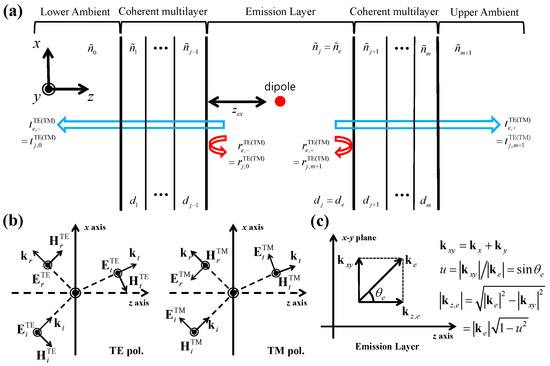
Figure 1.
(a) Schematic diagram of the organic light-emitting diode (OLED) multilayer micro-cavity (MMC) structure. (b) Sign configuration of the transverse electric (TE)- and transverse magnetic (TM)-polarized electric and magnetic field amplitudes on reflection and transmission based on the Verdet convention. (c) Schematic diagram of the wave vector components in the emission layer (EML).
In Figure 1a, and can be determined from the system reflection and transmission coefficients between layer j and layer m + 1(0), which can be iteratively calculated as [22]
In order to derive the formula for the NF absorption in the MMC structure, we refer to a mathematical procedure that derives the electric field amplitude in a dielectric/metal interface system [18] and add new terms that consider two-beam and multi-beam interferences. According to the classical electromagnetism, the electric field of an electric oscillating dipole can be expressed as a superposition of plane and evanescent waves [23,24], where is an angular frequency. Through the plane wave expansion, the electric fields in an infinite homogeneous medium and an MMC system can be written as
Here, represents the vertical (horizontal) dipole orientation, and is the magnetic permeability in free space. The term refers to basis vectors for TE and TM polarizations, which are
In Equations (8) and (10), are the reflection coefficients in reference to the location of the dipole emitter, and we have
We can derive the total radiated power from Equations (7)–(10). If we assume that the dipole emitter is immersed in a boundless EML, the total emitted power is expressed as [23]
where and c are the electric permittivity and the speed of light in free space. In the case of the MMC system, the total radiation power is derived as
Dividing Equations (13) and (14) by in Equation (12), we obtain the dimensionless relative radiated power F, also known as the Purcell factor [12], which is given by
Here, we use the normalized in-plane wave vector instead of and , which is convenient to consider the projection of the wave vector on the x-y plane and is better for simple calculations [12,14,18]. The differential can be replaced by in the spherical coordinate, where is the azimuth angle. If we assume that the dipole is randomly oriented in the horizontal direction, the radiation loses its azimuthal dependence. In Equation (15), the so-called spectral power density per normalized in-plane wave vector , which is also dimensionless, can be expressed with respect to the polarization and dipole orientation as follows [12,14,22].
If the dipole orientation is isotropic, the spectral power density can be expressed as [21,22]
Let us derive an analytical formula of the spectral response caused by the NF absorption, which becomes noticeable when the normalized in-plane wave vector u is very large. If we assume u is large enough, the z component of the total wave numbers in the (j − 1)-th, j-th, and (j + 1)-th layers can be approximately expressed as
Here, we use the relation of and which holds when it is assumed that . In addition, the exponential terms in Equations (3)–(6) become zero at the large value of u, written as
.
The system reflection coefficients in Equations (3) and (4), if u is large enough, can be written as
where we use the relation of in Equations (19)–(21).
When Equations (26) and (27) are inserted into Equation (17), the TM-polarized spectral power densities caused by the NF absorption are expressed as
where the modified TM-polarized reflection coefficients with a very large value of u are
and When u is large enough, the TE-polarized spectral power density originating from the NF absorption is written as
where the reflection coefficients of in Equations (24) and (25) are used.
3. Calculation Results
Figure 2 shows the multilayer structure of a top-emitting OLED, which is taken from [25]. The device is composed of 100-nm Ag as a reflective bottom anode, 250-nm Alq3 (tris-(8-hydroxyquinoline) aluminum) as an EML, 37-nm Ag as a semi-transparent top cathode, and 87-nm N, N-bis(naphthalen-1-yl)-N, N-bis(phenyl)-benzidine (NPB) as the capping layer. All results are calculated at the wavelength of λ = 520 nm, which corresponds to the photoluminescence peak of Alq3 in the literature [6]. The complex refractive indices of the materials shown in Figure 2 are obtained from the literature [26,27]. As organic materials in an OLED have relatively similar refractive indices [28,29,30], it is sometimes considered that all organic layers such as the electron transport layer and EML have the same refractive index value [31] or assumed that all the organic layers are integrated into the one organic layer. In Figure 2, it is assumed that both exciton generation and carrier transport occur at the EML. This simple structure of the top-emitting OLED is better to show the calculation results and optical analysis, which makes it easier and more intuitive for readers to understand the theoretical model and analysis of the NF absorption. The dipole emitter assumes to have a delta function distribution, which is positioned zex away from the interface between the Ag reflective bottom anode and EML.
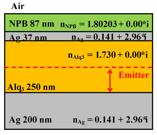
Figure 2.
Device structure of a top-emitting OLED along with the corresponding layer thickness and complex refractive index. To simplify the calculation, both exciton generation and carrier transport are assumed to occur at the Alq3 EML layer. The dipole emitter with the wavelength of 520 nm is assumed to be isotropic and to have the δ-distributed emission zone, which is positioned zex away from the interface between the reflective bottom anode and EML.
Figure 3 shows the calculated spatial profiles of the normalized electric field intensity of TM modes confined in the top-emitting OLED. The arrows indicate three dipole emitter positions, which will be used in the calculation results of Figure 4. These spatial profiles of the TM modes are calculated based on the boundary mode analysis performed by a commercial software of COMSOL Multiphysics [32]. The validity of the calculated eigenvalues and eigenfunctions obtained by the boundary mode analysis is confirmed through the agreement of the calculation results obtained by our homemade simulation code based on the transfer matrix method-based waveguide analysis of the OLED [21,33]. As shown in Figure 3, all TM modes are closely confined near the Ag metal/organic interfaces, which shows a typical characteristic of SP modes. Effective mode indices of three TM modes are shown in Table 1. The terms TM0, TM1, and TM2 are named in the ascending order of the real part of their effective mode index shown in Table 1. The imaginary part of the effective mode index corresponds to the extinction coefficient of each TM mode. The real parts of all the effective mode indices in Table 1 are greater than , which also confirms that all the TM modes in this top-emitting OLED structure are SP mode-like confined mode [21].
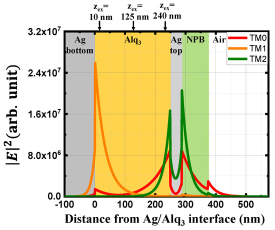
Figure 3.
Spatial distributions of the normalized electric field intensities of TM modes confined in the top-emitting OLED. Three TM modes, having a typical characteristic of surface plasmon (SP) modes, are denoted as TM0, TM1, and TM2, which are named in the ascending order of the real part of their effective mode index shown in Table 1. The arrows indicate three dipole emitter positions, which will be used in the calculation results of Figure 4.
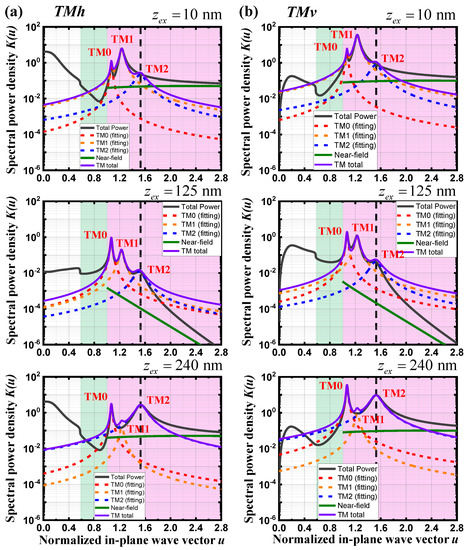
Figure 4.
The calculated TM-polarized power dissipation spectra at three dipole emitter positions for (a) horizontal and (b) vertical dipole orientations. Three spectral responses of the TM modes (TM0, TM1, and TM2) are fitted to the summation of the respective Lorentzian line shape function represented in Equation (30). The spectral response caused by the near-field (NF) absorption is calculated based on Equation (28) and plotted in the evanescent spectral range of u > 1.

Table 1.
Effective mode indices of TM modes obtained by the boundary mode analysis.
According to the analytical technique to identify planar WG and SP modes in OLEDs, the spectral responses of the SP-like TM modes can be approximated by the summation of the respective Lorentzian line shape function [21,34]
where and denote the phase index and extinction coefficient of the l-th confined SP-like TM mode, which corresponds to the real and imaginary parts of the effective mode index. The term represents the excitation magnitude and can be determined by the best fitting to the calculation result of the total spectral power density emitted by the horizontally (vertically) oriented dipole emitter, as will be shown in Figure 4.
Figure 4 shows the calculation results of the TM-polarized power dissipation spectra at three dipole emitter positions for horizontal and vertical dipole orientations. The validity of these calculation results is verified through a very good agreement with the calculated power dissipation spectra at the same structure of the top-emitting OLED obtained by a commercial software of SETFOS [35]. As shown in Figure 3, two dipole emitter positions are close to either bottom (zex = 10 nm) or top (zex = 240 nm) Ag metal layers, and the remaining one is located at the middle of the two Ag metal layers (zex = 125 nm). The white-, green-, and magenta-shaded regions refer to the light coupling mechanisms of the air mode WG mode and evanescent modes, respectively. Three spectral peaks of the SP-like TM modes (TM0, TM1, and TM2) are fitted to the summation of the respective Lorentzian line shape function in Equation (30). To verify the accuracy of the Lorentzian line-shaped spectral responses for the SP-like TM modes, the values of the effective mode index obtained by the best fitting to the total power dissipation spectrum are summarized in Table 2. Irrespective of the dipole positions, the real and imaginary parts of the effective mode index for three TM modes in Table 2 are nearly the same as those calculated by the boundary mode analysis in Table 1. This agreement confirms the validity of the Lorentzian line-shaped spectral responses of three SP-like TM modes obtained by the best fitting to the total power dissipation spectrum.
Table 2.
Effective mode indices of TM modes obtained by the Lorentzian line shape-based fitting to the total power dissipation spectrum.
In Figure 4, the aggregate spectral power density of the SP-like TM modes, obtained by summing all the spectral responses of three TM modes, is significantly different from the total spectral power density calculated based on Equation (17) in the evanescent region of u > 1. For the dipole positions of zex = 10 and 240 nm, the aggregate spectral power density of three SP modes is less than the total spectral power density at the spectral region of u > 1.523, which corresponds to the spectral peak position of the SP-like TM2 mode. In contrast, the aggregate spectral power density caused by three SP modes is greater than the total spectral power density when the dipole position is zex = 125 nm. In Figure 4, the spectral response of the NF absorption, calculated based on Equation (30), is also plotted in the evanescent region of u > 1. For all the dipole positions, the spectral response of the NF absorption becomes closer to the total spectral power density at the larger normalized in-plane wave vectors. Thus, the contribution of the NF absorption to the total power dissipation spectrum becomes more important than that of the SP modes when the in-plane wave vector becomes very large in the evanescent region.
To further investigate how the dipole emitter position in the EML affects the power dissipation of the dipole emitter, the relative radiated power of all the optical modes is calculated. The polarization-dependent relative optical power of each optical mode induced by a dipole emitter together with the total power dissipation is calculated by [9,12]
where indicates the normalized in-plane wave vector for the critical angle. In general, the optical power dissipation of the air mode is divided into the out-coupled air mode and absorption loss [22,36]. In Equations (32) and (33), the spectral power densities of the out-coupled air mode and the absorption loss are expressed as [36]
Here, and are the transmittance and reflectance from the EML to the upper ambient (air).
In Equation (34), only the WG mode is considered as the TE-polarized trapped light because TE-polarized light cannot excite the SP mode as well as the NF absorption [16,22]. In contrast, the TM-polarized trapped light is divided into the WG mode, SP mode, and NF absorption, of which spectral ranges are designated in Equations (35)–(37), respectively. In Figure 4, it is noticeable that Lorentzian line-shaped spectral responses of the SP modes can be larger than the total spectral power density at the WG spectral range of ucrit < u < 1, which are observed at the emitter positions of zex = 10 and zex = 240 nm. Hence, we integrate the total spectral power density rather than to calculate the relative radiated power of the WG mode in Equation (34).
Figure 5 shows the calculated relative radiative powers of all the optical modes as a function of the dipole emitter position in the EML for a horizontally oriented dipole radiating TM-polarized light, a vertically oriented dipole radiating TM-polarized light, a horizontally oriented dipole radiating TE-polarized light, and an isotropically oriented dipole. In Figure 5c, the relative radiated powers of the SP mode and the NF absorption are not included because they cannot be excited by the horizontally oriented dipole in the TE-polarized light [18,26]. The accuracy of these calculation results is verified through a very good agreement with a so-called modal analysis, power fraction of all the optical modes, as a function of the dipole position in the EML, which is calculated by a commercial software of SETFOS at the same structure of the top-emitting OLED [35].
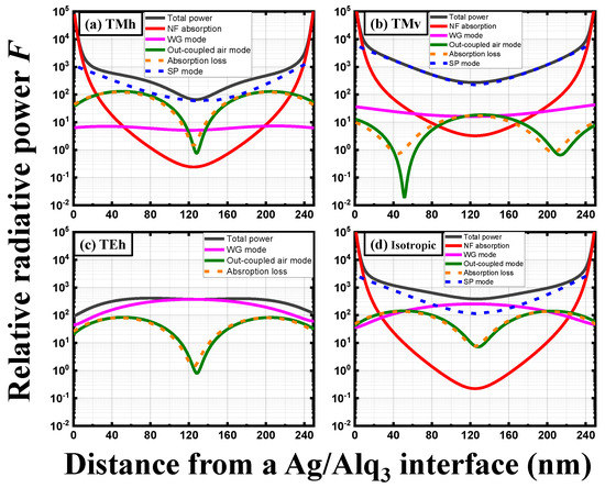
Figure 5.
Calculated relative radiative powers of all the optical modes as a function of the dipole position in the EML for (a) a horizontally oriented dipole radiating TM-polarized light (TMh), (b) a vertically oriented dipole radiating TM-polarized light (TMv), (c) a horizontally oriented dipole radiating TE-polarized light (TEh), and (d) an isotropically oriented dipole. For the horizontally oriented dipole radiating TE-polarized light, the relative radiated powers of the SP mode and the NF absorption are not included because they cannot be excited by the horizontally oriented dipole in the TE-polarized light.
In Figure 5, it is noticeable that the relative radiative power of the absorption loss has a similar trend to that of the out-coupled air mode. In other words, they either increase or decrease simultaneously as the dipole position is varied. According to Equations (38)–(40), the relative radiative power of the absorption loss is obtained by the subtraction of that of the out-coupled air mode from the total relative radiated power of the air mode radiated at the emitter position. Correspondingly, the relative radiative powers of the out-coupled air mode and the absorption loss are proportional to the total relative radiative power of the air mode radiated at the emitter position. In addition, we recently investigated the physical origin of the absorption loss based on the internal power flow of the air mode, where the absorption loss results from a part of the internal power flow of the air mode dissipated at the absorptive layer before the air mode is out-coupled into the air [25]. Thus, the variation in the relative radiative power of the absorption loss is similar to that in the relative radiative power of the out-coupled air mode as the dipole position is shifted.
In Figure 5a, it is also observed that the TM-polarized relative radiative power of the SP mode is very close to total relative radiative power. Furthermore, the TM-polarized relative radiative power of the SP mode is almost identical to total relative radiative power in Figure 5b. According to Equation (36), the relative radiative power of the SP mode is obtained by integrating the spectral power density, shown in Figure 4, from u = 1 to infinity such that the optical power contribution of the SP mode is more significant than the other modes such as the air mode having the spectral range from u = 0 to ucrit. In addition, according to the quantum-mechanical approach of the optical model of OLEDs, the optical power dissipation of each optical mode is determined by the amplitude of the electric field intensity at the emitter position and the photonic density of states of each optical mode [21]. In general, the SP mode has a relatively very large photonic density of states due to its very low group velocity [21]. Correspondingly, the contribution of the SP mode can be predominant in the TM-polarized relative radiative power. Similarly, the contribution of the WG mode is very significant in the relative radiative power of the horizontally oriented dipole radiating TE-polarized light, shown in Figure 5c, because the photonic density of states of the WG mode is relatively very larger than that of the air mode. Finally, in the case of the vertically oriented dipole radiating TM-polarized light, its dipole radiation pattern designated in Equation (11) refers to a large value of u, which corresponds to the spectral range of the SP mode [37,38]. Hence, the relative radiative power of the SP mode is almost identical to total relative radiative power in Figure 5b.
In Figure 5a,b, the TM-polarized relative radiative power emitted by the vertically oriented dipole is more coupled to the evanescent wave of SP modes and NF absorption than that radiated by the horizontally oriented dipole. On the other hand, the vertically oriented dipole provides smaller relative radiative power to both the out-coupled air mode and absorption loss than the horizontally oriented dipole does. This fact results from the angular radiation pattern of a Hertzian dipole emitter [12,14,22]. Regarding the out-coupled air mode and absorption loss, the relative radiative power emitted by the horizontally oriented dipole has the maximum intensities at the emitter positions of around 50 and 200 nm and the minimum intensity at the emitter position of around 130 nm. In contrast, the relative radiative power radiated from the vertically oriented dipole has the opposite emitter position of the maximum and minimum intensities. This out-of-phase difference of maximum and minimum intensities between horizontally and vertically oriented dipoles is ascribed to the combined effects of the phase difference induced by the Ag metal anode and the initial phase relation of the emitted electric fields [39]. On the other hand, the TM-polarized relative radiative power coupled to the SP modes steadily increases as the dipole emitter moves from the middle of the EML (zex = 125 nm) to the bottom (zex = 0 nm) or top (zex = 250 nm) EML/Ag interface in both horizontal and vertical dipole orientations.
In Figure 5a,b, the relative radiative power coupled to the NF absorption is extremely small at the middle of the EML (zex = 125 nm). As the dipole emitter shifts toward the EML/Ag interfaces, the relative radiative power coupled to the NF absorption dramatically increases. When the distance between the dipole emitter and the EML/Ag interface is less than 10 nm, the relative radiative power coupled to the NF absorption becomes predominant over the other optical modes and the relative radiative power coupled to the NF absorption converges to the total relative radiative power. These calculation results indicate that the contribution of the NF absorption should be considered in the analysis of the exciton power dissipation when the dipole position is close to the dielectric/metal interface. In addition, we find that the relative radiative power coupled to the NF absorption becomes minimized at the middle of two organic/metal interfaces in the top-emitting OLED, which is different from the previous result that the relative radiative power coupled to the NF absorption keeps decreasing as the dipole emitter moves away from a single organic/metal interface [18]. On the other hand, it is noticeable that the relative radiative power coupled to the NF absorption is symmetric in reference to the middle of two organic/metal interfaces, as shown in Figure 5. This is ascribed to the fact that the 250-nm Alq3 EML is sandwiched between the same metallic materials of the 100-nm Ag bottom anode and the 37-nm Ag semi-transparent top cathode, although their respective thicknesses are different in the device structure of the top-emitting OLED in Figure 2. However, this symmetric relative radiative power pattern of the NF absorption cannot be observed if the refractive indices of the materials sandwiching the EML are different.
Randomly patterned nanostructured metallic electrodes have been applied to OLEDs with the micro-cavity effect alleviated, which enables the broadband and angle-independent out-coupling enhancement of the WG mode with minimized surface plasmonic loss [40,41]. As our theoretical model of the NF absorption is applicable to and intended for OLEDs with planar metallic electrodes, it will not be directly applied to OLEDs with randomly patterned metallic electrodes. Similarly to solar cells with a randomly patterned metallic nanostructure [42], the localized SP mode will be excited in OLEDs with randomly patterned metallic electrodes, of which the theoretical calculation will be able to be performed through numerical simulations such as the finite-difference time domain.
In the case of transparent OLEDs with thin metallic electrodes [43], the excitation intensity of the SP mode will decrease because a part of the light will pass through the other electrode without strong light reflection and move back to the thin metallic electrode. According to the calculation results in Figure 5, the relative radiative power coupled to the NF absorption is proportional to that coupled to the SP modes. Thus, the total relative radiative power of the NF absorption and its influence will decrease in the case of transparent OLEDs.
4. Conclusions
We presented a theoretical modeling and analysis of the contribution of the NF absorption to the dipole power dissipation in a top-emitting OLED. The analytical formulation of the relative optical power coupled to the NF absorption was derived in the MMC structure based on the plane wave expansions of the electric field amplitude at large in-plane wave vectors. The dipole radiation power coupled to the NF absorption was noticeable for TM polarization and negligible for TE polarization. In the evanescent spectral region (u > 1), the spectral responses caused by the SP modes and NF absorption were compared in reference to the total spectral power density in the top-emitting OLED. The Lorentzian line-shaped spectral responses of the SP modes, obtained by the best fitting to the total spectral power density, were well matched with the total spectral response near the spectral peaks in the evanescent spectral region. On the other hand, the spectral responses of the SP modes significantly deviated from the total spectral power density at larger normalized in-plane vectors, where the spectral response originating from the NF absorption became predominant and approached the total spectral power density. Finally, the variation in the relative radiative powers coupled to the out-coupled air mode, absorption loss, WG mode, SP mode, and NF absorption was calculated as a function of the dipole emitter position in the EML. The relative radiative power coupled to the NF absorption became predominant over the other dissipation mechanisms when the distance between the dipole emitter and the EML/Ag interface was less than 10 nm. In addition, the relative radiative power coupled to the NF absorption became minimized at the middle of two organic/metal interfaces in the top-emitting OLED, which was different from the previous calculation result that the relative radiative power coupled to the NF absorption dramatically decreased as the dipole emitter moved away from a single organic/metal interface. Our theoretical modeling and analysis of the NF absorption will provide a deeper fundamental understanding of the exciton dissipation mechanism and can stimulate an experimental measurement of the NF absorption in OLEDs.
Author Contributions
Conceptualization, J.K. (Jungho Kim); methodology, J.K. (Jiyong Kim) and J.K. (Jungho Kim); software, J.K. (Jiyong Kim); validation, J.K. (Jiyong Kim) and J.K. (Jungho Kim); formal analysis, J.K. (Jiyong Kim) and J.K. (Jungho Kim); investigation, J.K (Jiyong Kim) and J.K. (Jungho Kim); writing—original draft preparation, J.K. (Jungho Kim); writing—review and editing, J.K. (Jiyong Kim) and J.K. (Jungho Kim); visualization, J.K. (Jiyong Kim) and J.K. (Jungho Kim); supervision, J.K. (Jungho Kim); project administration, J.K. (Jungho Kim); funding acquisition, J.K. (Jungho Kim). All authors have read and agreed to the published version of the manuscript.
Funding
This research was supported by the Basic Science Research Program through the National Research Foundation of Korea (NRF) funded by the Ministry of Education (grant number: NRF-2018R1D1A1B07047249).
Institutional Review Board Statement
Not applicable.
Informed Consent Statement
Not applicable.
Data Availability Statement
Not applicable.
Conflicts of Interest
The authors declare no conflict of interest.
References
- Mitsas, C.L.; Siapkas, D.I. Generalized matrix method for analysis of coherent and incoherent reflectance and transmittance of multilayer structures with rough surfaces, interfaces, and finite substrates. Appl. Opt. 1995, 34, 1678–1683. [Google Scholar] [CrossRef]
- Benisty, H.; Stanley, R.; Mayer, M. Method of source terms for dipole emission modification in modes of arbitrary planar structures. J. Opt. Soc. Am. A 1998, 15, 1192–1201. [Google Scholar] [CrossRef]
- Cho, H.; Yun, C.; Yoo, S. Multilayer transparent electrode for organic light-emitting diodes: Tuning its optical characteristics. Opt. Express 2010, 18, 3404–3414. [Google Scholar] [CrossRef]
- Mladenovski, S.; Hofmann, S.; Reineke, S.; Penninck, L.; Verschueren, T.; Neyts, K. Integrated optical model for organic light-emitting devices. J. Appl. Phys. 2011, 109, 083114. [Google Scholar] [CrossRef]
- Park, M.J.; Son, Y.H.; Kim, G.H.; Lampande, R.; Bae, H.W.; Pode, R.; Lee, Y.K.; Song, W.J.; Kwon, J.H. Device performances of third order micro-cavity green top-emitting organic light emitting. Org. Electron. 2015, 26, 458–463. [Google Scholar] [CrossRef]
- Kang, K.; Lee, Y.; Kim, J.; Lee, H.; Yang, B. A generalized Fabry–Pérot formulation for optical modeling of organic light-emitting diodes considering the dipole orientation and light polarization. IEEE Photon. J. 2016, 8, 1600519. [Google Scholar] [CrossRef]
- Song, J.; Kim, K.-H.; Kim, E.; Moon, C.-K.; Kim, Y.-H.; Kim, J.-J.; Yoo, S. Lensfree OLEDs with over 50% external quantum efficiency via external scattering and horizontally oriented emitters. Nat. Commun. 2018, 9, 3207. [Google Scholar] [CrossRef]
- Salehi, A.; Fu, X.; Shin, D.-H.; So, F. Recent advances in OLED optical design. Adv. Funct. Mater. 2019, 29, 1808803. [Google Scholar] [CrossRef]
- Meerheim, R.; Furno, M.; Hofmann, S.; Lüssem, B.; Leo, K. Quantification of energy loss mechanisms in organic light-emitting diodes. Appl. Phys. Lett. 2010, 97, 253305. [Google Scholar] [CrossRef]
- Chance, R.R.; Prock, A.; Silbey, R. Molecular fluorescence and energy transfer near metal interfaces. In Advances in Chemical Physics; Wiley: Hoboken, NJ, USA, 1978; pp. 1–65. [Google Scholar]
- Barnes, W.L. Fluorescence near interfaces: The role of photonic mode density. J. Mod. Opt. 1998, 45, 661–699. [Google Scholar] [CrossRef]
- Furno, M.; Meerheim, R.; Hofmann, S.; Lüssem, B.; Leo, K. Efficiency and rate of spontaneous emission in organic electroluminescent devices. Phys. Rev. B 2012, 85, 115205. [Google Scholar] [CrossRef]
- Brütting, W.; Frischeisen, J.; Schmidt, T.D.; Scholz, B.J.; Mayr, C. Device efficiency of organic light-emitting diodes: Progress by improved light outcoupling. Phys. Status Solidi A 2013, 210, 44–65. [Google Scholar] [CrossRef]
- Kim, J.; Kim, K.-Y.; Kim, J. Generalized Poynting vector model to calculate the spatial and spectral profiles of the electric field intensity, optical power flow, and optical absorption for all optical modes of organic light-emitting diodes. Opt. Express 2019, 27, A1261–A1286. [Google Scholar] [CrossRef]
- Hobson, P.A.; Wasey, J.A.E.; Sage, I.; Barnes, W.L. The Role of surface plasmons in organic light-emitting diodes. IEEE J. Sel. Topics Quantum Electron. 2002, 8, 378–386. [Google Scholar] [CrossRef]
- Furno, M.; Gather, M.C.; Lüssem, B.; Leo, K. Coupled plasmonic modes in organic planar microcavities. Appl. Phys. Lett. 2012, 100, 253301. [Google Scholar] [CrossRef]
- Fuchs, C.; Will, P.-A.; Wieczorek, M.; Gather, M.C.; Hofmann, S.; Reineke, S.; Leo, K.; Scholz, R. Enhanced light emission from top-emitting organic light-emitting diodes by optimizing surface plasmon polariton losses. Phys. Rev. B 2015, 92, 245306. [Google Scholar] [CrossRef]
- Penninck, L.; Mladenowski, S.; Neyts, K. The effects of planar metallic interfaces on the radiation of nearby electrical dipoles. J. Opt. 2010, 12, 075001. [Google Scholar] [CrossRef]
- Jeon, S.; Lee, S.; Han, K.-H.; Shin, H.; Kim, K.-H.; Jeong, J.-H.; Kim, J.-J. High-quality white OLEDs with comparable efficiencies to LEDs. Adv. Opt. Mater. 2018, 6, 1701349. [Google Scholar] [CrossRef]
- Cho, C.; Greenham, N.C. Computational study of dipole radiation in re-absorbing perovskite semiconductors for optoelectronics. Adv. Sci. 2021, 8, 2003559. [Google Scholar] [CrossRef] [PubMed]
- Kang, K.; Kim, K.-Y.; Kim, J. Theoretical comparison of the excitation efficiency of waveguide and surface plasmon modes between quantum-mechanical and electromagnetic optical models of organic light-emitting diodes. Opt. Express 2018, 26, A955–A973. [Google Scholar] [CrossRef]
- Neyts, K.A. Simulation of light emission from thin-film microcavities. J. Opt. Soc. Am. A 1998, 15, 962–971. [Google Scholar] [CrossRef]
- Lukosz, W. Theory of optical-environment-dependent spontaneous-emission rates for emitters in thin layers. Phys. Rev. B 1980, 22, 3030–3038. [Google Scholar] [CrossRef]
- Setälä, T.; Kaivola, M. Decomposition of the point-dipole field into homogenous and evanescent parts. Phys. Rev. E 1999, 59, 1200–1206. [Google Scholar] [CrossRef]
- Kim, J.; Kim, J.; Kim, K.-Y. Theoretical modeling of the internal power flow and absorption loss of the air mode based on the proposed Poynting vector analysis in top-emitting organic light-emitting diodes. J. Korean Phys. Soc. 2018, 73, 1663–1674. [Google Scholar] [CrossRef]
- Kang, K.; Yoon, J.; Kim, J.; Lee, H.; Yang, B. Effect of the finite pixel boundary on the angular emission characteristics of top-emitting organic light-emitting diode. Opt. Express 2015, 23, A709–A717. [Google Scholar] [CrossRef] [PubMed]
- Pyo, B.; Joo, C.W.; Kim, H.S.; Kwon, B.-H.; Lee, J.-I.; Lee, J.; Suh, M.C. A nanoporous polymer film as a diffuser as well as a light extraction component for top emitting organic light emitting diodes with a strong microcavity structure. Nanoscale 2016, 8, 8575–8582. [Google Scholar] [CrossRef]
- Li, W.; Jones, R.A.; Allen, S.C.; Heikenfeld, J.C.; Steckl, A.J. Maximizing Alq3 OLED internal and external efficiencies: Charge balanced device structure and color conversion outcoupling lenses. J. Disp. Technol. 2006, 2, 143–152. [Google Scholar] [CrossRef]
- Callens, M.K.; Yokoyama, D.; Neyts, K. Anisotropic materials in OLEDs for high outcoupling efficiency. Opt. Express 2015, 23, 21128–21148. [Google Scholar] [CrossRef] [PubMed]
- Salehi, A.; Chen, Y.; Fu, X.; Peng, C.; So, F. Manipulating refractive index in organic light-emitting diodes. ACS Appl. Mater. Interfaces 2018, 10, 9595–9601. [Google Scholar] [CrossRef] [PubMed]
- Youn, W.; Lee, J.W.; Yu, H.; Kim, D.Y. Effect of Refractive Index Contrast on Out-Coupling Efficiency of Corrugated OLEDs using Low-Refractive-Index LiF Interlayer. ACS Appl. Electron. Mater. 2020, 2, 2218–2223. [Google Scholar] [CrossRef]
- COMSOL Multiphysics, Version 5.2.; Comsol Inc.: Burlington, MA, USA, 2016; Available online: http://www.comsol.com (accessed on 22 December 2020).
- Revelli, J.F.; Tutt, L.W.; Kruschwitz, B.E. Waveguide analysis of organic light-emitting diodes fabricated on surfaces with wavelength-scale periodic gratings. Appl. Opt. 2005, 44, 3224–3237. [Google Scholar] [CrossRef] [PubMed]
- Revelli, J.F. Excitation of waveguide modes in organic light-emitting diode structures by classical dipole oscillators. Appl. Opt. 2006, 45, 7151–7165. [Google Scholar] [CrossRef]
- Fluxim, A.G. Semiconducting Emissive Thin Film Optics Simulator SETFOS; Winterthur: Zürich, Switzerland; Available online: http://www.fluxim.com (accessed on 8 January 2021).
- Kim, J.; Kang, K.; Kim, K.-Y.; Kim, J. Origin of a sharp spectral peak near the critical angle in the spectral power density profile of top-emitting organic light-emitting diodes. Jpn. J. Appl. Phys. 2018, 57, 012101. [Google Scholar] [CrossRef]
- Flämmich, M.; Gather, M.C.; Danz, N.; Michaelis, D.; Bräuer, A.H.; Meerholz, K.; Tünnermann, A. Orientation of emissive dipoles in OLEDs: Quantitative in situ analysis. Org. Electron. 2010, 11, 1039–1046. [Google Scholar] [CrossRef]
- Kang, K.; Kim, J. Effect of dipole orientation on the angular emission characteristic of a three-dimensional top-emitting organic light-emitting diode with square pixel boundary. J. Korean Phys. Soc. 2019, 74, 649–659. [Google Scholar] [CrossRef]
- Kim, J.; Kim, K.-Y.; Kim, J. Optical modeling of the emission zone profile and optimal emitter position based on the internal field profile of the air mode in organic light-emitting diodes. Appl. Opt. 2018, 57, 8394–8406. [Google Scholar] [CrossRef]
- Xu, L.-H.; Ou, Q.-D.; Li, Y.-Q.; Zhang, Y.-B.; Zhao, X.-D.; Xiang, H.-Y.; Chen, J.-D.; Zhou, L.; Lee, S.-T.; Tang, J.-X. Microcavity-free broadband light outcoupling enhancement in flexible organic light-emitting diodes with nanostructured transparent metal-dielectric composite electrodes. ACS Nano 2016, 10, 1625–1632. [Google Scholar] [CrossRef]
- Ou, Q.-D.; Xu, L.-H.; Zhang, W.-Y.; Li, Y.-Q.; Zhang, Y.-B.; Zhao, X.-D.; Chen, J.-D.; Tang, J.-X. Light outcoupling enhanced flexible organic light-emitting diodes. Opt. Express 2016, 24, A674–A681. [Google Scholar] [CrossRef]
- Nishijima, Y.; Rosa, L.; Juodkazis, S. Surface plasmon resonances in periodic and random patterns of gold nano-disks for broadband light harvesting. Opt. Express 2012, 20, 11466–11477. [Google Scholar] [CrossRef] [PubMed]
- Zhang, Y.-B.; Ou, Q.-D.; Li, Y.-Q.; Chen, J.-D.; Zhao, X.-D.; Wei, J.; Xie, Z.-Z.; Tang, J.-X. Transparent organic light-emitting diodes with balanced white emission by minimizing waveguide and surface plasmonic loss. Opt. Express 2017, 25, 15662–15675. [Google Scholar] [CrossRef]


Publisher’s Note: MDPI stays neutral with regard to jurisdictional claims in published maps and institutional affiliations. |
© 2021 by the authors. Licensee MDPI, Basel, Switzerland. This article is an open access article distributed under the terms and conditions of the Creative Commons Attribution (CC BY) license (https://creativecommons.org/licenses/by/4.0/).