Abstract
Chemical–mechanical polishing (CMP) is a process that planarizes semiconductor surfaces and is essential for the manufacture of highly integrated devices. In CMP, pad conditioning using a disk with diamond grit is adopted to maintain the surface roughness of the polishing pad and remove polishing debris. However, uneven pad wear by conditioning is unavoidable in CMP. In this study, we propose a contact-area-changeable conditioning system and utilize it to conduct a preliminary study for improving pad lifetime. Using the conventional conditioning method (Case I), the material removal rate (MRR) decreased rapidly after 12 h of conditioning and the within-wafer non-uniformity (WIWNU) increased. However, the results of conditioning experiments show that when using a contact-area-changeable conditioning system, uniform pad wear can be obtained in the wafer–pad contact area and the pad lifetime can be extended to more than 20 h. Finally, the newly proposed conditioning system in this study may improve the CMP pad lifetime.
1. Introduction
In the semiconductor manufacturing process, chemical mechanical polishing (CMP) is becoming more important as the integration of semiconductor devices increases [1,2,3,4,5]. CMP is a process that involves simultaneous chemical reactions and mechanical material removal, enabling the formation of interlayer dielectrics (ILD) [6,7,8], shallow trench isolation (STI) [6,9,10], metal wiring [11,12,13,14], and metal contacts [15,16,17] through the global planarization of thin films. In CMP, a wafer is attached to a carrier, and a polishing pad is attached to a platen, as shown in Figure 1. The polishing head presses the wafer onto the polishing pad, and, simultaneously, the platen and polishing head are rotated in the same direction. During CMP, a slurry comprising abrasive particles and chemicals is supplied to the polishing pad through a slurry supply system. The chemical elements in the slurry cause a chemical reaction to the thin film on the surface of the wafer, and planarization occurs as abrasive particles remove the chemically reacted thin film [18,19,20].
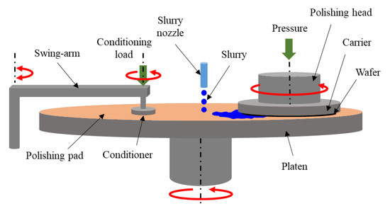
Figure 1.
Schematic illustration of chemical–mechanical polishing (CMP) and swing-arm conditioning system.
Pad conditioning is performed using a disk with diamond grit (diamond conditioner) during CMP to remove polishing debris and maintain the surface roughness of the polishing pad [21,22,23,24,25]. The polishing pad for CMP is primarily manufactured from polyurethane and contains pores and grooves for slurry flow [26,27]. Without pad conditioning, the CMP debris will accumulate in the pore on the polishing pad surface after CMP, resulting in pad glazing [28,29]. Pad glazing reduces the material removal rate (MRR) of the CMP process and yields defects such as scratches. Pad conditioning ensures the quality of CMP by preventing defects while maintaining a constant MRR. Recently, the industry has generally used a swing-arm-type conditioning system where the arm swings around the axis of rotation (Figure 1). Major parameters determining the results of swing-arm conditioning include conditioning pressure, rotational speed of conditioner, swing speed of swing-arm, and design of conditioner.
However, pad wear is unavoidable because a diamond conditioner is used in swing-arm pad conditioning [30,31]. In particular, uneven pad wear affects the MRR and within-wafer non-uniformity (WIWNU). Chang et al. [32] proposed a mathematical model of oscillation-type CMP conditioning. They used dimensionless parameters to perform integration in the calculation of sliding distances of diamond grits. Chen et al. [33] also proposed a mathematical model for oscillation-type CMP conditioning. They found that the smaller the radius of the diamond conditioner compared to the radius of the polishing pad, the higher the uniformity of the pad profile. However, the proposed methods in the studies of Chang et al. and Chen et al. were not applicable in swing-arm conditioning.
According to Zhou et al. [34], pad conditioning generally results in a “W”-shaped pad profile. They simulated the pad wear profile with a mathematical approach based on the geometry and moving motions during swing-arm CMP conditioning. According to their experiment, the profile of the polishing pad was related to the profile of MRR at CMP, and they showed that the shape of the polishing pad profile and the MRR profile had the opposite shape. They explained that the difference between experimental result and simulation may come from the moment that the friction forces act on the conditioner disk. Lee et al. [35] simulated swing-arm CMP conditioning via kinematic modeling and showed that the swing-arm velocity profile (SAVP) affected the pad profile. They calculated the pad wear profile by drawing a virtual concentric circle on the surface of the pad and summing the sliding distance of the conditioner’s diamond grits passing through the virtual area. They considered five cases of SAVP and found that the convex-shaped SAVP aided in the flatness of the polishing pad during CMP conditioning. Li et al. [30] also predicted pad profile after CMP conditioning by using a surface element method. They reported that the difference between the predicted pad profile and the pad profile measured by the experiment may come from the set-up of the experiment, the deformation of the pad, and the surface unevenness. Lee et al. [36] investigated the relationship between pad profile after pad conditioning and CMP results (MRR and WIWNU) using a pad measurement system (PMS). They discovered that the average depth of pad wear affected the MRR and that the maximum depth of pad wear affected the WIWNU. According to Lee et al., the concave-shaped profile of a conditioner’s duration time in swing-arm conditioning can enhance the pad lifetime. Lee et al. [37] discovered that the results of the pad-wear experiment based on a uniformly shaped grit conditioner were more similar to those of kinematic modeling than those based on a randomly shaped grit conditioner. Tyan [38] demonstrated that the profile of the polishing pad can be changed based on the area density of the diamond grit in the conditioner and the arrangement of the grits, and that the smaller the conditioner-radius-to-pad-radius, the flatter the pad profile. Chen et al. [39] proposed a surface metrology monitoring method by using a chromatic confocal sensor. They showed that the pad non-uniformity (PU) was related to pad effective lifetime index (PELI).
Previous studies involving pad wear profiles in swing-arm conditioning attempt to improve the uniformity of the polishing pad wear by adjusting the swing speed (or duration time) of the arm and the conditioner design. However, the swing motion adjustment in swing-arm conditioning and the conditioner design cannot prevent a “W”-shaped pad profile, and profile control is restricted. In this study, we compared a newly developed split conditioning system and the conventional conditioning system in terms of the polishing pad lifetime.
2. Experimental Set-Up
2.1. CMP Conditioning System and Condition
Figure 2 shows the design of the CMP conditioning system incorporated with a split conditioner. In the newly designed CMP conditioning system, the pneumatic cylinder controls the height of the conditioner. The conventional CMP conditioner (SAESOL DIAMOND Ind. Co. Ltd., Ansan, Korea) is separated by waterjet cutting. The conditioner comprises an inner conditioner and an outer ring-type conditioner.
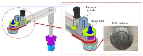
Figure 2.
Swing-arm conditioning system and split conditioner used in this study.
The diameter of the inner conditioner was 64 mm, and the width of the outer ring-type conditioner was 31 mm. The gap between the two conditioners was 2.5 mm. The loads acting on the inner and outer conditioners were independently controllable and rotated at the same rotational speed using a rotary joint.
The rotational speeds of the platen and conditioner were 93 and 101 rpm, respectively. The conditioning load was 4 kgf. The swing-arm’s swing count was fixed at nine sweeps per minute. The specific conditioning conditions are listed in Table 1.

Table 1.
Conditions for CMP conditioning.
The swing-arm’s swing movement was partitioned into five zones in the radial direction above the polishing pad. The CMP conditioning system used in the experiment regulated the swing motion of the conditioner with the duration time (%) in the zones above the polishing pad. In this study, the same conditioner duration time was used throughout the entire zone to exclude the effect of the swing motion on the pad wear profile. Table 2 shows the conditioner duration times in the conditioning zones.
Table 2.
Swing condition of conditioner.
2.2. Pad Wear Simulation
In this study, the numerical analysis method proposed by Lee et al. [35] was used to simulate the pad wear profile. In their proposed method, virtual grids are created on the polishing pad, and the number of passing diamond grits attached to the conditioner in the rectangular area is counted to predict the pad wear profile. Figure 3 and Figure 4 show the schematic illustration and the flowchart of the pad wear profile simulation. The calculation of the pad wear profile was conducted with LabView (National Instrument Corp., Austin, TX, USA) software.
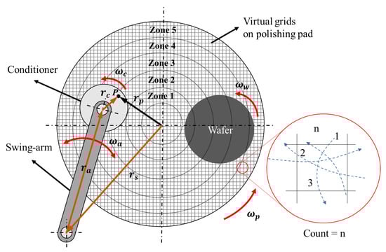
Figure 3.
Schematic illustration of pad wear profile simulation.
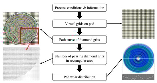
Figure 4.
Flowchart of pad wear profile simulation.
In Figure 3, P means an arbitrary point on the conditioner disk. rp and rs are the position vectors of the position P on the conditioner and rotating axis of swing-arm relative to the pad. ra and rc are the local position vectors of conditioner rotating center and the position P on the conditioner. ωc, ωa, ωp, and ωw are angular velocity vectors of conditioner, swing-arm, pad, and wafer, respectively. The rp can be calculated from Equation (1) [35].
During the simulation, the total number of diamond grits on the conventional conditioner was 468 ea. For the split conditioner, the numbers of diamond grits on the inner and outer ring-type conditioners were 200 and 268 ea, respectively. It was assumed that the diamond grit on the conditioner was evenly arranged and the polishing pad in its initial state was ideally flat. The unit density inspection area was 10 mm2. For a fair comparison with the experimental results, the pad wear simulation was performed with 1 h of conditioning. The calculation interval was set to 0.01 s in the pad wear profile simulation. The radial profile of the pad cut rate profiles was calculated for comparison with the experimental results. In this study, the conditioning conditions of four cases were considered, as shown in Table 3.
Table 3.
Conditioning cases considered in this study.
2.3. CMP Experiment and Pad Profile Measurement
In this study, CMP experiments with SiO2-deposited (1.5 μm thick) Si wafers (200 mm in diameter) were conducted to verify the pad lifetime after pad conditioning. The pad lifetime was defined as the usage duration of the polishing pad until the groove of the polishing pad had worn out, or when an abrupt change in the MRR and WIWNU occurred.
An R&D CMP machine (POLI-762, G&P Technology Inc., Busan, Korea) was used for the CMP experiments. A hard polyurethane pad (KONI pad from KPX Chemical, Seoul, Korea) and a silica slurry (TSO-12, Soulbrain Co., Ltd., Seongnam, Korea) were prepared. During CMP, the location of the wafer center was fixed at 230 mm from the center of the polishing pad. Hence, the wafer contacted the polishing pad from 150 to 350 mm in the radial direction from the center of the polishing pad. The wafer and retaining-ring pressures were 34.3 and 44.1 kPa, respectively. The rotational speeds of the polishing head and platen were 87 and 93 rpm, respectively. The CMP experimental conditions are listed in Table 4.
Table 4.
CMP experimental conditions.
The thickness of the SiO2 film was measured using a reflectometer (ST5030-SL, K-Mac, Daejeon, Korea, Measurement range: 10 nm~35 μm). The MRRs of the SiO2 films were measured at 39 points in the radial direction of the wafers. The edge exclusion in the measurement of the MRR was 7 mm.
After pad conditioning, the pad profile was measured using a pad measurement system (PMS, G&P Technology, Busan, Korea, Resolution: 0.1 μm, Repeatability <2% (1σ)) (Figure 5). The PMS uses an active displacement sensor and transports the sensor using a linear motion guide and servo motor. To measure the deviation in the thickness of the polishing pad, the PMS measured the profile of the platen first and used it as a reference. The pad profile was measured from the center to the edge of the polishing pad, and the signal (thickness of pad) from the sensor was transmitted to the computer with information regarding the radial position of the pad. The pad cut rate distribution was obtained from the pad thickness profiles before and after conditioning.
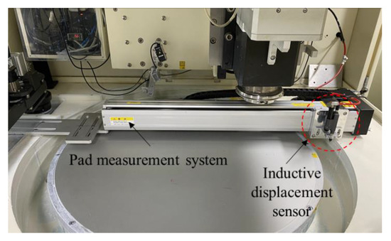
Figure 5.
Pad measurement system (PMS, G&P Technology, Busan, Korea).
Figure 6 shows the procedure of the experiment. First, the polishing pad was attached to the platen and the initial pad profile was measured with the pad measurement system. The first conditioning was performed for 1 h, and the first CMP experiment using SiO2 wafer was conducted after conditioning. After the first CMP, CMP experiments were performed after 1, 2, or 3 h of conditioning. The experiment was conducted for up to 20 h of cumulative conditioning time, but the experiment was stopped when the wafer was broken due to excessive pad wear.
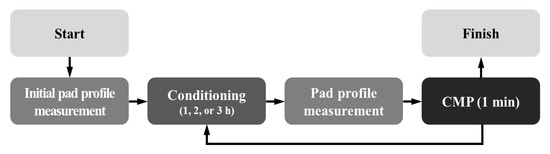
Figure 6.
Procedure of conditioning and CMP experiment.
3. Result and Discussion
3.1. Simulation Results of Pad Cut Rate Distribution
The split conditioner proposed herein was compared with the disk-type conditioner (full contact) used for conventional CMP conditioning. The swing conditions of the conditioner used in the simulations are shown in Table 2. In the simulations, the conditioning time was 1 h, and the radial distribution of the pad wear rate was expressed by counting the number of times that the diamond grit of the conditioner passed a 10 mm × 10 mm square drawn virtually on the polishing pad.
Figure 7a–d show the simulation results of swing-arm pad conditioning. Figure 7a shows the pad cut rate profile when using the conditioner used in the general CMP process. Lee et al. [36] discovered that the average depth of the pad and the maximum depth of pad wear affected the MRR and WIWNU, respectively. If the condition of Case I is used in CMP conditioning, then the uniform wear of abrasive pads cannot be avoided. In particular, significant pad wear was observed in the section where the 200 mm diameter wafer used in this study (distance from pad center: 150–350 mm) was placed. The pad cut rate was obtained in the contact area of the wafer with the pad, as shown in Figure 7b, when the inner conditioner in Zones 2–5 was used to reduce excessive pad wear. Cases III and IV using the inner and outer ring-type conditioners exhibited considerable waviness in the pad cut rate profiles, as shown in Figure 7c,d, respectively. These results appear to be due to the possibility of obtaining a flatter pad profile if the conditioner has a smaller radius than the abrasive pad radius, as in Tyan’s study [38].
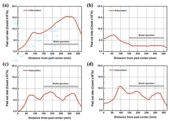
Figure 7.
Simulation result of pad cut rate distribution: (a) Case I (reference), (b) Case II, (c) Case III, and (d) Case IV.
The average values of the pad cut rate in the radial direction and the wafer–pad contact area of the four conditioning cases are shown in Figure 8a,b. Simulation results show that Case I with the conventional conditioning disk yielded a high average pad cut rate, whereas Case II yielded the lowest average pad cut rate among the four cases. Cases III and IV indicated a lower average pad cut rate than Case I, but the pad cut rate profile in the wafer–pad contact area exhibited waviness.
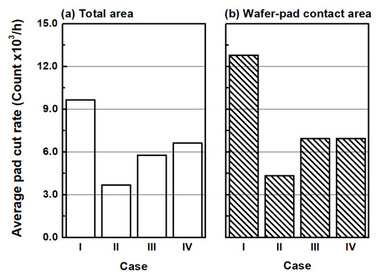
Figure 8.
Average pad cut rate of conditioning cases: (a) total area and (b) wafer–pad contact area.
Figure 9 shows the maximum pad cut rate for the five conditioning cases. Figure 9a shows the maximum pad cut rate in the radial direction, and Figure 9b shows the maximum pad cut rate of the wafer–pad contact area. As shown in Figure 9a,b, the maximum pad cut rate in Case I was the highest, and Case II had the lowest maximum pad cut rate. In Case II, the inner conditioner, which had a small diameter, was used to reduce pad wear in Zones 2–5; consequently, excessive pad wear was shown in Case I, and the flatness of the pad cut rate profile improved using both the inner and outer ring-type conditioners in Zone 1. In the next section, we present the experimental study performed to investigate the pad lifetimes of Cases I and II.
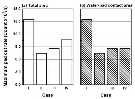
Figure 9.
Maximum pad cut rate of conditioning cases: (a) total area and (b) wafer–pad contact area.
3.2. Comparison of Pad Lifetimes
Prior to the marathon experiment on CMP conditioning, we conducted experiments on the pad cut rate profiles of Cases I and II. The conditioning experiment was conducted using the same method as the simulation conditions, and, after the experiment, the thickness profile of the polishing pad was measured using the PMS. In this study, the results were normalized using each average value to compare the experimental and simulation results. In the experiment, the pad cut rate profile was obtained from the difference in pad thickness profiles before and after conditioning. Figure 10 and Figure 11 show the normalized simulated and experimental pad cut rate profiles of Cases I and II, respectively. Experiments confirmed that the simulated pad cut rate profile exhibited a shape similar to that of the pad cut rate profile measured in the experiment. In the range of 0 to 25 mm, the variation in measured signal is not large because grooves do not exist on the surface of the polishing pad. The jagged pad profile in the range of 25 mm or more is due to grooves on the polishing pad surface. The difference between the simulation and experimental results at both ends of the profile appeared to be due to the time delay during the right and left turns of the swing-arm. Furthermore, as Zhou [34] claimed, the difference between simulation and experimental results appears to be due to the moment caused by friction between the conditioner and the pad due to the gimbaled joint of the conditioner.
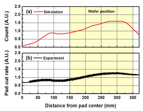
Figure 10.
Normalized pad cut rate profile of Case I: (a) simulation result and (b) experimental result.
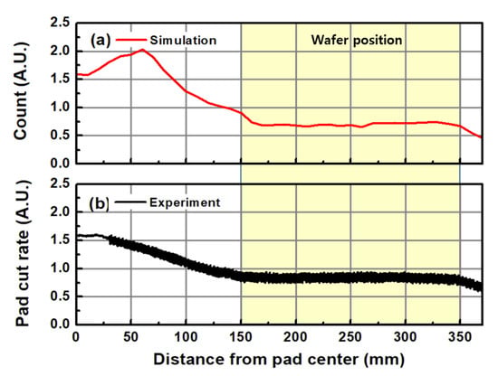
Figure 11.
Normalized pad cut rate profile of Case II: (a) simulation result and (b) experimental result.
In the marathon experiment on CMP conditioning, the pad profile was measured using the PMS after conditioning, and the slurry was supplied continuously during conditioning. The conditioning conditions are shown in Table 1 of Section 2.1. To determine the lifetime of the abrasive pad, CMP tests were conducted using 200-mm-diameter SiO2 wafers, and the MRR and WIWNU were measured. The equations for the MRR and WIWNU are as shown in Equations (2) and (3), respectively.
where σ and MRRavg represent the standard deviation of the MRR and average MRR, respectively.
Figure 12 shows the pad thickness and profile change after conditioning for Case I. The average pad cut rate in Case I was 43.4 μm/h based on the experimental result. Similar to the simulation results, the maximum pad wear in the pad profile occurred at a position 250 to 300 mm from the pad’s center. In particular, pad wear was significant in areas where the wafer and polishing pad were in contact with each other. As shown in Figure 13, Case II had a lower pad cut rate (22.2 μm/h) than Case I and exhibited a flat pad profile in the wafer–pad contact area. As shown in Figure 12 and Figure 13, the pad profile was generally tilted, but the CMP polishing head exhibited a gimbal structure that enabled it to resemble the tilted surface of the pad when it established contact with the wafer.
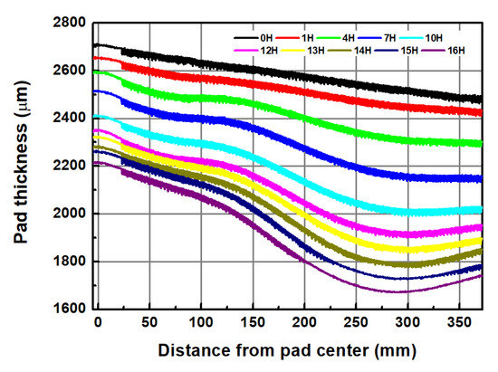
Figure 12.
Pad thickness and profile change after conditioning for Case I.
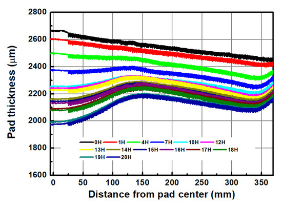
Figure 13.
Pad thickness and profile change after conditioning for Case II.
The CMP experiment was conducted for 1 min immediately after conditioning, and the conditions of the experiment are shown in Table 4. Figure 14 illustrates the MRR distribution of the SiO2 film after conditioning for Cases I (Figure 14a) and II (Figure 14b). In Case I, after 16 h of conditioning, the grooves on the pad wore out in the wafer–pad contact area, and the wafer broke during the CMP experiment. Meanwhile, conditioning experiments for Case II were conducted for up to 20 h.
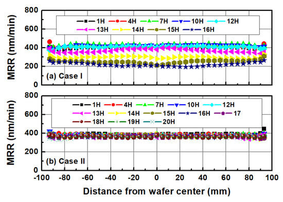
Figure 14.
Material removal rate distribution as a function of conditioning time: (a) Case I and (b) Case II.
Figure 15 and Figure 16 show the MRR and WIWNU for Cases I and II, respectively, based on the conditioning time. For Case I, the MRR decreased by approximately 44.9% from 401.3 to 221.0 nm/min during 16 h of conditioning. As shown in Figure 15, in Case I, the decrease in the MRR occurred rapidly after 12 h of conditioning. Meanwhile, in Case II, the MRR was reduced by approximately 7.4% from 387.7 to 359.0 nm/min during 20 h of conditioning. Figure 16 shows the WIWNU as a function of conditioning time. Similar to the MRR in Case I, the WIWNU remained within 3% during 12 h of conditioning and increased rapidly thereafter. In Case II, the WIWNU remained within 3% for up to 20 h, and the polishing pad was available for a longer duration compared with Case I. According to Lee et al. [34], locally excessive pad wear causes a non-uniform stress distribution on the wafer during CMP. The rapid decrease in the MRR and the increase in the WIWNU after 12 h of conditioning in Case I may be due to the non-uniform stress distribution caused by locally excessive pad wear. In Case II, the pad profile in the wafer–pad contact area was relatively flat even after 20 h of conditioning, which would result in less change in the MRR and WIWNU.
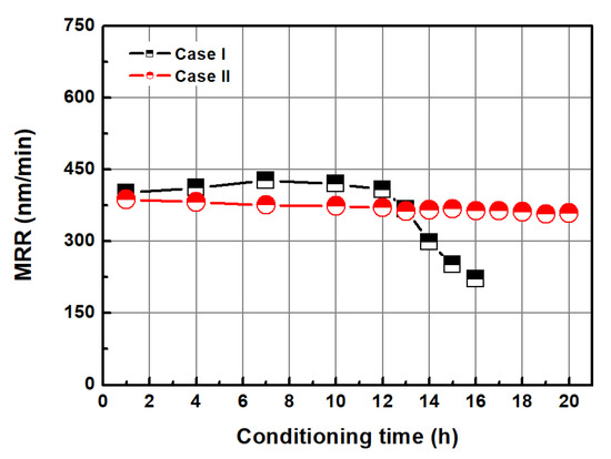
Figure 15.
Average material removal rates of Case I and II as a function of conditioning time.
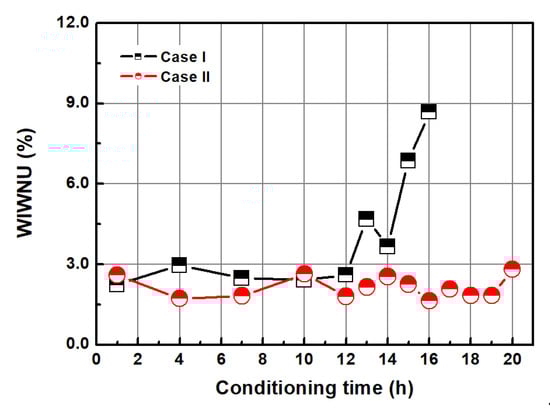
Figure 16.
Within-wafer non-uniformities of Case I and II as a function of conditioning time.
Figure 17a–c show the scanning electron microscope (SEM) images of the cross-sections of the polishing pads in the wafer–pad contact area. Figure 17a–c show the cross-sectional views of the as-received polishing pad, polishing pad after the experiment for Case I, and polishing pad after the experiment for Case II, respectively. For Case II, the pad grooves remained after 20 h of conditioning, whereas for Case I, which had been conditioned for 16 h, all of the grooves on the pads disappeared after the experiment.
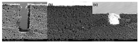
Figure 17.
Scanning electron microscope (SEM) images of the cross-sections of polishing pads in the wafer–pad contact area: (a) as-received, (b) after conditioning for Case I, and (c) after conditioning for Case II.
While previous studies on polishing pad profiles after pad conditioning have been focused on conditioner characteristics and swing motion of the conditioning arm, this study suggests improvement of polishing pad profiles by changing the contact area between the conditioner and polishing pad. Although this study differs from the existing studies in that it demonstrates that using the contact-area-changeable CMP conditioning system can increase the life of polishing pads, it seems that additional research on contact area changes of diamond conditioners and experiments under more diverse conditioning process conditions will be needed. Further, a study on the cleaning of the conditioner to remove slurry in the space between the boundaries of the divided conditioner will likely be required.
4. Conclusions
In this study, we investigated contact-area-changeable swing-arm conditioning for enhancing pad lifetime. The difference between this study and existing studies is not the adjustment of process parameters but, rather, the improvement of the conditioning system, which provides a way to increase the life of the polishing pad. The proposed conditioning system was incorporated with a split conditioner designed to enable independent contact with the polishing pad during conditioning. First, we analyzed the pad cut rate profile using the numerical analysis method, and, among the four cases considered in this study, Case II exhibited a flat pad cut rate profile in the wafer–pad contact area.
In the conditioning and CMP experiments, Case II, involving a contact-area-changeable conditioner, was compared with Case I, involving a conventional CMP conditioner. Experiments showed that, for Case I, locally excessive pad wear occurred in the pad–wafer contact area. Owing to the uneven pad wear in the wafer–pad contact area by conditioning, the MRR of the SiO2 CMP in Case I began decreasing after 12 h of conditioning, whereas the WIWNU increased. In Case II, the wafer–pad contact area in Zones 2–5 was reduced, where excessive pad wear occurred in Case I. In Case II, the MRR and WIWNU remained the same until 20 h of conditioning. Experiments showed that maintaining uniform pad wear in the wafer–pad contact area using contact-area-changeable conditioning can improve the pad lifetime.
The new conditioning system proposed herein can improve the CMP pad lifetime. Further studies regarding the effects of various process parameters should be conducted using the contact-area-changeable conditioning system.
Author Contributions
Conceptualization, H.L.; Investigation, J.S. and H.L.; Project administration, H.L.; Supervision, H.L.; Writing: original draft, J.S.; Writing: review and editing, H.L.; Funding Acquisition, H.L. All authors have read and agreed to the published version of the manuscript.
Funding
Please add: This research was supported by the BB21+ Project in 2020 and Basic Science Research Program through the National Research Foundation of Korea (NRF), funded by the Ministry of Education (NRF-2018R1D1A1B07043169).
Institutional Review Board Statement
Not applicable.
Informed Consent Statement
Not applicable.
Data Availability Statement
Data sharing is not applicable to this article.
Acknowledgments
We thank G&P Technology Inc. for the support for the experiment.
Conflicts of Interest
The authors declare no conflict of interest.
References
- Verkatesh, V.C.; Inasaki, I.; Toenshof, H.K.; Nakagawa, T.; Marinescu, I.D. Observations on Polishing and Ultraprecision Machining of Semiconductor Substrate Materials. CIRP Ann. Manufact. Technol. 1995, 44, 611–618. [Google Scholar] [CrossRef]
- Zhao, G.; Wei, Z.; Wang, W.; Feng, D.; Xu, A.; Liu, W.; Song, Z. Review on modeling and application of chemical mechanical polishing. Nanotechnol. Rev. 2020, 9, 182–189. [Google Scholar] [CrossRef]
- Zantye, P.B.; Kumar, A.; Sikder, A.K. Chemical mechanical planarization for microelectronics applications. Mater. Sci. Eng. R Rep. 2004, 45, 89–220. [Google Scholar] [CrossRef]
- Krishnan, M.; Nalaskowski, J.W.; Cook, L.M. Chemical Mechanical Planarization: Slurry chemistry, Materials, and Mechanism. Chem. Rev. 2010, 110, 178–204. [Google Scholar] [CrossRef] [PubMed]
- Jeong, S.; Jeong, K.; Choi, J.; Jeong, H. Analysis of Correlation between Pad Temperature and Asperity angle in Chemical Mechanical Planarization. Appl. Sci. 2021, 11, 1507. [Google Scholar] [CrossRef]
- Huang, D.; Babu, S.V.; Wang, L.; Moser, T. Effect of CMP Pad and Slurry to STI and ILD Polishing. ECS Trans. 2010, 33, 23. [Google Scholar] [CrossRef]
- Guo, D.M.; Liu, R.H.; Kang, R.K.; Jin, Z.J. Study on Adhesion Removal Model in CMP SiO2 ILD. Key Eng. Mater. 2008, 389–390, 475–480. [Google Scholar] [CrossRef]
- Bengochea, L.V.; Smapuruno, T.; Kavaljer, M.; Johnston, R.; Philipossian, A. Characterization of CMP Slurries Using Densitometry and Refractive Index Measurements. Micromachines 2018, 9, 542. [Google Scholar] [CrossRef]
- Chang, S.-H. A dishing model for STI CMP process. Microelectron. Eng. 2005, 82, 136–142. [Google Scholar] [CrossRef]
- Xie, X.; Park, T.; Boning, D.; Smith, A.; Allard, P.; Patel, N. Characterizing STI CMP Processes with an STI Test Mask Having Realistic Geometric Shapes. MRS Online Proc. Libr. 2004, 816, 941–948. [Google Scholar] [CrossRef]
- Ryan, J.G.; Geffken, R.M.; Poulin, N.R.; Paraszczak, J.R. The evolution of interconnection technology at IBM. IBM J. Res. Dev. 1995, 39, 371–381. [Google Scholar] [CrossRef]
- Fayolle, M.; Romagna, F. Copper CMP evaluation: Planarization issue. Microelectron. Eng. 1997, 37–38, 135–141. [Google Scholar] [CrossRef]
- Wenbio, R.; Lan, C.; Zhigang, L.; Tuanchun, Y. Effects of pattern characteristics on copper CMP. J. Semicond. 2009, 30, 046001. [Google Scholar] [CrossRef]
- Ein-Eli, Y.; Starosvetsky, D. Review on copper chemical-mechanical polishing (CMP) and post-CMP cleaning in ultra large system integrated (ULSI)—An electrochemical perspective. Electrochim. Acta 2007, 52, 1825–1838. [Google Scholar] [CrossRef]
- Lee, W.-S.; Kim, S.-Y.; Seo, Y.-J.; Lee, J.-K. An optimization of tungsten plug chemical mechanical polishing (CMP) using different consumables. J. Mater. Sci. Mater. Electron. 2001, 12, 63–68. [Google Scholar] [CrossRef]
- Fayolle, M.; Sicurani, E.; Morand, Y. W CMP process integration: Consumables evaluation-electrical results and end point detection. Microelectron. Eng. 1997, 37–38, 347–352. [Google Scholar] [CrossRef]
- Tseng, W.-T.; Mohan, K.; Hull, R.; Hagan, J.; Truong, C.; Lehuu, D.K.; Muradian, D. A Microreplicated Pad for Tungsten Chemical-Mechanical Planarization. ECS J. Solid State Sci. Technol. 2016, 5, P546. [Google Scholar] [CrossRef]
- Seo, J. A review on chemical and mechanical phenomena at the wafer interface during chemical mechanical planarization. J. Mater. Res. 2020, 36, 235–257. [Google Scholar] [CrossRef]
- Lee, H. Semi-empirical Material Removal Model with Modified Real Contact Area for CMP. Int. J. Precis. Eng. Manufact. 2019, 20, 1325–1332. [Google Scholar] [CrossRef]
- Banerjee, G.; Rhoades, L. Chemical Mechanical Planariaation–Historical Review and Future Direction. ECS Trans. 2008, 13, 1–19. [Google Scholar] [CrossRef]
- Borucki, L.J.; Witelski, T.; Plwase, C.; Kramer, P.R.; Schwedeman, D. A theory of pad conditioning for chemical–mechanical polishing. J. Eng. Math. 2004, 50, 1–24. [Google Scholar] [CrossRef]
- Lee, W.J.; Park, H.S.; Shin, H.C. Enhancement of CMP pad lifetime for shallow trench isolation process using profile simulation. Curr. Appl. Phys. 2009, 9, S134–S137. [Google Scholar] [CrossRef]
- Sun, T.; Borucki, L.; Zhuang, Y.; Philipossian, A. Investigating the effect of diamond size and conditioning force on chemical mechanical planarization pad topography. Microelectron. Eng. 2010, 87, 553–559. [Google Scholar] [CrossRef]
- Tsai, M.Y.; Peng, J.D. Investigation of a novel diamond disk’s effect on pad topography in oxide chemical mechanical polishing. Mater. Manuf. Proc. 2010, 25, 1440–1448. [Google Scholar] [CrossRef]
- Tso, P.L.; Ho, S.Y. Factors influencing the dressing rate of chemical mechanical polishing pad conditioning. Int. J. Adv. Manuf. Technol. 2007, 33, 720–724. [Google Scholar] [CrossRef]
- Jeong, H.D.; Park, K.H.; Cho, K.K. CMP Pad Break-in Time Reduction in Silicon Wafer Polishing. CIRP-Ann. 2007, 56, 357–360. [Google Scholar] [CrossRef]
- Tso, P.-L.; Huang, Z.-H.; Chou, S.-W.; Shih, C.-Y. Study on the CMP Pad Life with Mechanical Properties. Key Eng. Mater. 2009, 389–390, 481–486. [Google Scholar] [CrossRef]
- Kim, N.-H.; Seo, Y.-J.; Lee, W.-S. Temperature effects of pad conditioning process on oxide CMP: Polishing pad, slurry characteristics, and surface reactions. Microelectron. Eng. 2006, 83, 362–370. [Google Scholar] [CrossRef]
- Tsai, M.-Y. Polycrystalline diamond shaving conditioner for CMP pad conditioning. J. Mater. Proc. Technol. 2010, 210, 1095–1102. [Google Scholar]
- Li, Z.C.; Baisie, E.A.; Zhang, X.H. Diamond disc pad conditioning in chemical mechanical planarization (CMP): A surface element method to predict pad surface shape. Precis. Eng. 2012, 36, 356–363. [Google Scholar] [CrossRef]
- Yeh, H.M.; Chen, K.S. Development of a pad conditioning simulation module with a diamond dresser for CMP applications. Int. J. Adv. Manuf. Technol. 2010, 50, 1–12. [Google Scholar] [CrossRef]
- Chang, O.; Kim, H.; Park, K.; Seo, H.; Jeong, H. Mathematical modeling of CMP conditioning process. Microelectron. Eng. 2007, 84, 577–583. [Google Scholar] [CrossRef]
- Chen, C.-Y.; Yu, C.-C.; Shen, S.-H.; Ho, M. Operational Aspects of Chemical Mechanical Polishing Polish Pad Profile Optimization. J. Electrochem. Soc. 2000, 147, 3922–3930. [Google Scholar] [CrossRef]
- Zhou, Y.Y.; Davis, E.C. Variation of polish pad shape during pad dressing. Mater. Sci. Eng. B 1999, 68, 91–98. [Google Scholar] [CrossRef]
- Lee, S.; Jeong, S.; Park, K.; Kim, H.; Jeong, H. Kinematical modeling of pad profile variation during conditioning in chemical mechanical polishing. Jpn. J. Appl. Phys. 2009, 48, 126502. [Google Scholar] [CrossRef]
- Lee, H.; Lee, S. Investigation of pad wear in CMP with swing-arm conditioning and uniformity of material removal. Precis. Eng. 2017, 49, 85–91. [Google Scholar] [CrossRef]
- Lee, D.; Lee, K.; Jeong, S.; Kim, H.; Cho, H.; Jeong, H. Effect of Diamond Abrasive Shape of CMP Conditioner on Polishing Pad Surface Control. Tribol. Lubr. 2019, 35, 330–336. [Google Scholar]
- Tyan, F. Pad Conditioning Density Distribution in CMP Process with Diamond Dresser. In Proceedings of the 2005 American Control Conference, Portland, OR, USA, 8–10 June 2005. ThA09.6. [Google Scholar]
- Chen, C.-C.A.; Li, J.-C.; Liao, W.-C.; Ciou, Y.-J.; Chen, C.-C. Dynamic Pad Surface Metrology Monitoring by Swing-Arm Chromatic Confocal System. Appl. Sci. 2021, 11, 179. [Google Scholar] [CrossRef]


Publisher’s Note: MDPI stays neutral with regard to jurisdictional claims in published maps and institutional affiliations. |
© 2021 by the authors. Licensee MDPI, Basel, Switzerland. This article is an open access article distributed under the terms and conditions of the Creative Commons Attribution (CC BY) license (https://creativecommons.org/licenses/by/4.0/).