Abstract
The state-of-the-art technology of X-ray microcalorimeters based on superconducting transition-edge sensors (TESs), for applications in astrophysics and particle physics, is reviewed. We will show the advance in understanding the detector physics and describe the recent breakthroughs in the TES design that are opening the way towards the fabrication and the read-out of very large arrays of pixels with unprecedented energy resolution. The most challenging low temperature instruments for space- and ground-base experiments will be described.
1. Introduction
Many space-based observatory and ground-based experiments in the field of astrophysics and particle-physics are improving dramatically their sensitivity and overall capabilities thanks to the use of large arrays of superconducting transition-edge sensor (TES) microcalorimeters [1,2,3,4,5,6,7,8].
A TES is a superconducting thin film that, due to its sharp superconducting-to-normal transition, can be used as an extremely sensitive thermometer. It is weakly coupled to a thermal bath at temperature lower than the TES critical temperature. When operating as a calorimeter, a TES is well coupled to a radiation absorber. By means of an ac or dc voltage bias circuit, it can be self-heated and kept stable within the transition. The current flowing in the TES provides the signal, which is amplified by inductively coupled superconducting quantum interference devices (SQUIDs). Researchers have attained a high level of understanding of the underlying detector physics. Thanks to this, several groups in the world have recently succeeded in optimally designing the detectors to enable the multiplexing, with exquisite energy resolution, of a large number of pixels both in dc-bias multiplexing schemes, like Time/Code Division Multiplexing (TDM/CDM) [9,10] and GHz-Frequency Division Multiplexing (GHz-FDM) [11], and ac-bias multiplexing schemes like MHz-Frequency Division Multiplexing (MHz-FDM) [12].
In this review, we will take a snapshot of the state-of-the-art of the TES microcalorimeter technology for soft X-ray instrumentations. Our work is built upon existing reviews [13,14,15], and it will focus more on the applications of TES in future X-ray space observatories and for experiments aiming to explore the new frontiers of physics.
The TES X-ray calorimeter technology is entering a new era where the fabrication of arrays with more than 1000 pixels is becoming a routine and instruments with almost one hundred of low temperature read-out channels are being build. The field is moving from experimental research towards fine and sophisticated cryogenic engineering to fabricate cutting-edge instruments for fundamental research, with the potential to build detectors with 100 kilo-pixels in the coming 20 years. To achieve the goals set by these ambitious projects, it is essential to further optimize the pixel design and to improve the efficiency of the available read-out technology. The sensor and the read-out are influencing each other and, when aiming to the highest level of performance, they cannot be developed separately. For these reasons, it is important to give an overview of the fundamental physical processes affecting the TES resistive transition and the noise, with the focus on the interaction between sensors and the read-out system. We will describe the major breakthrough, after the last review [15], on the TES design optimization, which opened the way to the read-out of large arrays of pixels.
This paper is organized as follows. In Section 2, we present the basic theory of TES microcalorimeters and discuss the physics of the resistive transition and the major noise sources. We will describe as well the generalized system of equations that can be solved to perform realistic simulations of the dynamical response of the TES and its read-out circuit. Thanks to the available computational power of modern computers, the end-to-end simulation will become an essential tool to guide the development and the calibration of the very complex instruments under construction.
In Section 3, the challenges in the fabrication of the sensors, absorbers, and thermal links in a large array are described. The vivid research work of the past few years in the improvement of the performance and uniformity of the TES X-ray calorimeters, both for the dc and ac voltage biased read-out, is covered in Section 4. Most of the development in this area is driven by the stringent requirements from the X-ray Integral Field Unit (X-IFU) [16], which is one of the two instruments of the Athena astrophysics space mission [2] approved by ESA in the Cosmic Vision 2015–2025 Science Programme.
In Section 5, we summarize the recent progress in the multiplexing demonstration of a large number of pixels with high energy resolution. Finally, in Section 6 we will describe several ground- and space-based applications where the core technology is based on large arrays of TES X-ray microcalorimeters.
2. TES Physics and Models
In this section, we will focus on the theory of TESs. We will discuss primarily the case of X-ray microcalorimeters. However, the theory presented is general enough to be adapted to other TES-based energy or power detectors.
A figure of merit that characterizes single photons detectors is the resolving power for photons with energy E. A fundamental limit for the minimum energy resolution achievable with a calorimeter is given by the random exchange of energy between the detector and the thermal bath [13]. This thermodynamic limit is given by . It depends quadratically on the temperature T of the calorimeter, linearly on the detector heat capacity C, and it is independent on the thermal conductance G of the thermal link. This value however does not set a limit to how accurately the thermal fluctuations can be measured. This can be understood by looking at the signal and noise power spectrum of the thermodynamic fluctuations. Each frequency bin provides an uncorrelated estimation of the signal amplitude and the signal-to-noise ratio can be improved as the square root of the number of bins averaged [13]. The two most important parameters used to estimate the detector signal-to-noise ratio and the energy resolution are the unit-less logarithmic temperature and current sensitivity and , calculated, respectively, at a constant current I and temperature T. They have been conveniently introduced [17] to parametrize the TES resistive transition
and they can be estimated experimentally at the quiescent operating point () in the transition. A detailed calculation of the minimum energy resolution achievable with a TES calorimeter is possible. After a careful analysis of the thermometer sensitivity, the detector noise and the signal bandwidth, gives
The unit-less parameter depends on the thermal conductance exponent n, which is related to the physical nature (radiative or diffusive) of the thermal link between TES and the heat sink at [13]. For a TES [14]. The parameter takes into account the non-linear correction terms to the linear equilibrium Johnson noise, which conveniently helps to write the Johnson voltage spectral density as . For a linear resistance . For a TES, it is usually defined as where the factor is the first order, near equilibrium, non-linear correction term as discussed in [18] and the unit-less factor parameterizes any unexplained observed deviation from this approximation. More details on this important noise contribution are given further in Section 2.3.
From Equation (2), it is clear that low heat capacity devices, operating at very low temperature , could achieve very high energy resolution. The C value, however, is not a free parameter and is typically defined by the dynamic range, , requirement of the specific application. By developing TES with a large temperature sensitivity , the photon energy can be measured with a much higher resolution than the magnitude set by thermodynamic fluctuations. To achieve then the ultimate sensitivity, for given C and , the factor has to be minimized.
The details of the TES electro-thermal response and noise will be discussed here below. In Section 2.1, we will review the recent development in the understanding of the physics of the TES resistive transition. The differential electrical and thermal equations describing a TES and its bias circuit are derived in Section 2.2, while an overview of the fundamental noise sources in a TES-based detector will be presented in Section 2.3, including the recent new insight on this topic.
A TES operates under voltage-bias condition in the negative electro-thermal feedback (ETF) mode. This guarantees stable operation and self-biasing within its sharp superconducting transition [19]. As we will see later on in this section, depending on the multiplexing technology chosen to read out a large array of pixels, a TES is dc voltage biased or ac voltage biased in the MHz range. While keeping the discussion as general as possible, we will place the emphasis on the MHz biased TESs for two reasons. The first one is due to the fact that it is the least considered case in the literature, since most of the phenomena observed under MHz bias have only been recently studied in the detail and understood. The second reason is that the MHz read-out (in-phase and quadrature) allows us to directly probe many of the TES physics effects discussed in Section 2.1.
2.1. The Proximity Effects and the Resistive Transition
A TES consists of a thin film made of a superconducting bilayer with an intrinsic critical temperature typically around . It is directly connected to superconducting bias leads with critical temperature . Figure 1a shows a schematic of a TES connected to the bias superconducting leads, while more details on the TES structures and their fabrication are reviewed in Section 3.
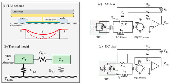
Figure 1.
(a) Schematic diagram of a TES bilayer connected to the bias leads and the absorber. The red curves represent the superconducting order parameter for an SS’S (solid) and a SNS (dashed) TES weak-link. (b) Thermal model of a TES-Absorber system () including a second thermal body . is the main thermal conductance to the bath, , and . (c,d) The electrical circuits for the ac and dc bias read-out, respectively.
It was first reported by Sadleir et al. [20,21] that TES structures behave as a superconducting weak-link due to the long-range longitudinal proximity effect (LoPE) originating from the superconducting Nb leads. Their conclusion was based on three solid experimental findings, namely (i) the exponential dependence of the critical current upon the TES length L and the square root of the temperature difference :
with for , (ii) the scaling of the effective transition temperature and the transition width as , and (iii) the Fraunhofer-like oscillations of the critical current as a function of the applied perpendicular magnetic field. The longitudinal proximity effect was observed over extraordinary long () distances and it is responsible for the enhancement, in the proximity of the leads, of the spatially varying superconducting order parameters of the TES bilayer, as shown in Figure 1a. It has been shown as well [21] that the order parameter is suppressed in proximity to normal metal structures deposited along or on top of the TES due to the lateral inverse proximity effect (LaiPE). Both the longitudinal and the lateral-inverse proximity effects can be used to fine tune the effective TES critical temperature . By measuring many devices with different geometries and aspect-ratios, fabricated from the same bilayer film, it is possible to separate the contribution of the longitudinal proximity effect from that of the lateral inverse proximity effect. In [22], for example, the effect of the Nb leads has been identified by measuring of TESs of equal width W, but different lengths L. The results are then used to correct for the longitudinal proximity effects and look at the lateral inverse proximity effects in the devices of varying widths.
Ridder et al. [23] have recently investigated the effects of the longitudinal proximity effects in Ti/Au TES structures using Ti and Nb superconducting leads material, with low and high respectively. A comparison was done with the previous results obtain with Mo/Au [21] and Mo/Cu [15] TESs. The measured characteristic length scale of the proximity effect was the lowest for the Ti/Au TES with Ti leads. The reported was about 2.5 higher for the Ti/Au TES with Nb leads, and almost 8 times higher for the MoAu TES with Nb leads.
The discovery of the proximity effects in TES structures naturally leads to treat these devices as superconducting SNS or SS’S weak-link, with the bilayer being N when or S’ when . Extensive reviews on the Josephson weak-links have been given by Likharev [24] and Golubov et al. [25]. The Josephson effect in SS’S junctions at arbitrary temperatures was analysed first by Kupriyanov and Lukichev [26,27] in the framework of the Usadel equations. They showed that for long junctions and the has an exponential dependence, as shown in Equation (3), with the effective coherence length larger than the intrinsic coherence length of the material:
Here, is the coherence length for the normal material N in the dirty limit, with the electronic diffusivity for a material with Fermi velocity and mean-free path . Equation (4) can be approximated as
For a 200 nm Au metal film at , with m/s and thickness limited , the diffusivity and the coherence length . When studying the physics of a TES, one has to keep in mind that its coherence length is enhanced by a factor due to the presence of the leads with a critical temperature and by the fact that the detector operates close to . For typical TESs, the coherence length can become much larger than .
A microscopic model of a TES as a weak-link has been developed by Kozorezov et al. [28] using the Usadel approach. Usadel equations have been used later on by Harwin et al. [29,30] to investigate the effect of lateral normal metal structures and to reproduce the TES current-to-voltage characteristics.
The most successful macroscopic model developed to describe Josephson junctions and superconducting weak-links of many different kind is the resistively and capacitively shunted junction (RCSJ) model. The overdamped limit () of the RSCJ model, namely the resistively shunted junction model (RSJ), was formalized by Kozorezov et al. [31] for a dc-biased TES. The RSJ model can be used to calculate analytically the TES resistive transition and to generalize the TES response to an alternating current. The most interesting prediction in this work is the existence of an intrinsic TES reactance, which can be calculated exactly. As we will see in Section 2.2, this has important implications on the TES response, in particular when operating under MHz voltage biasing.
Using the Smoluchowski equation approach for quantum Brownian motion in a tilted periodic potential in the presence of thermal fluctuations [32], an analytical solution for the dependency of the TES resistance on temperature and current was found [31]. In the limit of zero-capacitance and small value of the quantum parameter, we can write:
with the normal state resistance, the ratio of the Josephson coupling to thermal energy, and . Here, is the critical Josephson current and and are the modified Bessel function of the complex order, , and real variable, z. An example of an curve calculated from Equation (6) is shown in Figure 2. By differentiating Equation (6), the parameters and are obtained:
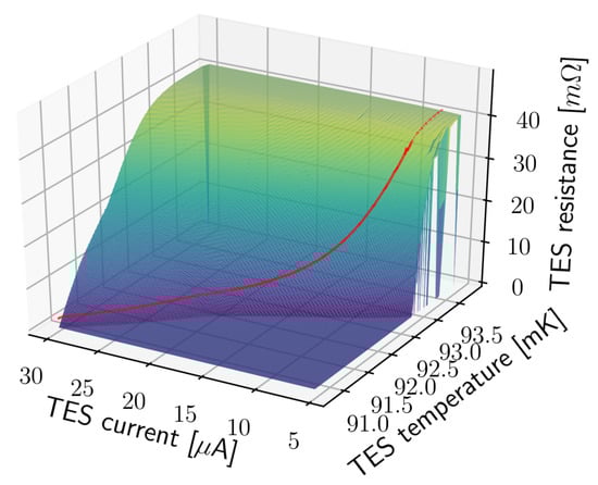
Figure 2.
Example of an R(T,I) curve calculated for an X-ray TES calorimeter developed for X-IFU. The red curve shows the TES bias trajectory.
A TES generally operates in the limit of (Josephson coupling energy larger than the thermal energy) and . The device is superconducting () for and normal () for . Under these conditions, the above equations and the relation between and can be greatly simplified following the work of Ambegaokar and Halperin [33]. The resistive transition can then be written as [34]
and and reduce to
A simple relation for the ratio holds:
which could turn out to be useful for the pixel design optimization [35].
The curve can be measured rather accurately, very close to , for many orders of magnitude of the current flowing in the TES [20]. By studying the shape of for different TES geometry and as a function of the perpendicular magnetic field , in relation with the TES bias current I, one can derive detailed information on the physical mechanism involved in a TES [20,21,34,35,36]. A careful TES current and voltage calibration is however required to accurately calculate the ratio at each bias point, which is needed to validate experimentally the resistive transition models. In [35], for example, the curve measured for small pitch TES X-ray calorimeters optimized for solar astronomy and with two different design, has shown a very good agreement with the Equation (12) derived from the RSJ model.
There exists a class of devices, where the weak-link effects described above are less dominant. TESs could for example operate in a stronger superconducting regime, depending on the exact shape of the and the bias current, which in turn depends on the device saturation power required by the applications. It has been reported [15], for example, that large Mo/Cu TESs, in size, with several normal metal features on top, operating at high bias current , and with the lead closer to the bilayer , typically show a curve which is well described by the Ginzburg–Landau (G-L) critical current. The latter takes the form:
where is the value of at zero temperature. These devices have typically lower and values than the ones predicted by the RSJ model (Equations (7) and (8)) [37]. The physical mechanism of phase slip lines (PSL) [38] has been proposed, in the simplified form of a two-fluid model [39,40], as a way to explain the resistive transition in devices where the ideal weak-link effects were not observed. The PSL model reproduces the general behaviour of the IV characteristic of these devices as a function of temperature and provides a better prediction of and in the transition. The PSL model has also been considered to explain kinks and steps observed along the transition in dc bias TESs [38] and is used to guide the optimization of X-ray detectors by studying the dependence of the transition width on the TES [41,42]. Bennett et al. [37] made a comparison, updated and expanded later on [15], between the RSJ and the PSL models for many TESs with different geometries. The predictions are not always consistent with all the data presented, and the influence of the TES geometry and the effect of the connected normal metal structures is still not clear. The main result of their comparison is that, over the range of operation of a TES, for TESs larger than , the measured curves are more consistent with Equation (13). On the contrary, Smith et al. [35] have shown, with pixels developed for solar astronomy application, that TESs as large as and with normal metal noise mitigation structure do follow the weak-link prediction as in Equations (3) and (12). It is clear that it is not always easy to discriminate between the regime of operation of a TES-based device, in particular in the presence of complicated normal metal structures affecting the current distribution in the TES bilayer.
As it will be discussed in Section 4.2, there is a wish to fabricate detectors that operate away from the weak-link regime to minimize non-ideal effects that can deteriorate the detector performance. This is particularly true for ac biased devices. It is then very important to understand the underlying physical mechanisms that shape the curve and the TES resistive transition. To predict the exact behaviour in the cross-over region between the RSJ and the phase-slip models, it might be necessary to solve the Usadel equations in 2D for a realistic TES design (with normal metal stems, bars, and stripes), as a follow up of the work done in one dimensional structures [29,30,31].
From the experimental point of view, the full characterization of the new generation of devices, discussed in Section 4, might help in the understanding of the resistive transition.
The theoretical framework reviewed by Likharev [24] and Golubov et al. [25] could guide the interpretation of the experimental data. As described in their work, the possible physical states in which a TES of different size likely operate can be illustrated in the diagram of Figure 3, simplified and reproduced after [24,43].
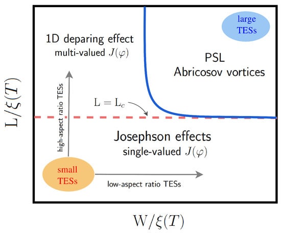
Figure 3.
Possible physical states in which a TES of different size likely operates. Reproduced after [24,43], by permission from American Physical Society and the authors.
The TES length L and width W are normalized with respect to the coherence length . The solid blue line shows the boundary between the regions of large size superconducting structures, where PSL/Abrikosov vortices could be formed, and the small weak-link where the pure Josephson effect is observed. The dashed red line corresponds to a TES critical length , estimated by Likharev to be , above which, for small TES width W, a transition from a Josephson effect, with single valued current-phase relation to a one-dimensional depairing state (phase slip centers), with multivalued current-phase relation, might occur. The exact shape and position of these boundaries are not trivial to calculate for a TES, since they depend on many parameters, such as the self magnetic field, the bilayer coherence length and the difference between the bilayer and the of the leads. The threshold is temperature dependent as well, so the TES might switch from a weak to a strong superconducting state depending on the actual bias conditions. We have seen before that for a TES with an Au thickness of , the coherence length close to could reach values, enhanced by the electrodes with , of . This leads to values of . This estimation, however, is rather approximated, since the cross-over boundary strongly depends on the current distributions, which in turn depend on the width and the thickness of the bilayer, as well as on the presence or not of normal metal structure in a real TES.
The common practice to discriminate whether a TES behaves as a weakly-linked or strong superconductor has been so far to look for the exponential behaviour of the , its Fraunhofer-like behaviour as a function of the perpendicular magnetic field, the oscillatory features in the TES reactance as a function of the MHz voltage bias TES [36], or the presence of Shapiro-steps in dc bias TES under MHz current or magnetic field excitation [44,45,46]. The latter effect, for example, manifest itself with a specific current step pattern in the TES curves at , according to the Josephson law. However, similar steps might be observable in large 2D superconducting films, with a non-exponential as in Equation (13), as a result of the coherent motion of a large number of Abrikosov vortices [24,38]. The characterization of the crossover from weak- to strong superconductivity behaviour is not trivial. A better way to identify the transition between the possible states, schematically shown in Figure 3, would be to measure experimentally the current-phase relation [25] of TESs with different geometry in a wide range of biasing condition. The ideal Josephson effect should take place only when is single-valued. For geometries where , is multi-valued and the TES might enter into a non-stationary state where depairing effects, phase slip, and PSL/Abrikosov vortex formation are likely to occur.
A study that deserves more attention is the modeling of the TES transition using the Berezinskii–Kosterlitz–Thouless (BTK) theory, which describes the onset of dissipation due to current assisted vortex pair unbinding. In a recent work based on a previous investigation done on TESs by Fraser [47], Fabrega et al. [48] have studied the resistive transition of Mo/Au bare TESs, with high 460–640 , as a function of temperature, current, and magnetic field. The observed large-current induced broadening of the transition at low resistance could be explained by the BTK mechanism. More investigations in this direction are needed, but this approach could prove useful to understand non-equilibrium effects in TESs and the transition from a weak-link to a 2D strong superconductivity regime.
2.2. TES Electro-Thermal Equations
The standard electro-thermal linear model for a dc biased TES calorimeter was originally developed by Lindeman et al. [49] to describe the noise and the response to photons. No assumption were made on the TES physics, and the resistance, for each bias point in the transition, was linearly approximated as in Equation (1). This model has been successfully used to understand the behaviour of TES-based detectors in many works that followed. In this section, we present the Langevin electro-thermal equations for a TES calorimeter, generalized for the dc and ac biased case, assuming the detector physics being well described by the Josephson effects, formalized in the RSJ model. A schematic diagram of the detector thermal model and the electrical ac and dc bias circuit is shown in Figure 1.
As suggested and observed in many experiments [50,51,52,53,54], a single-body thermal model for a TES calorimeter is rarely sufficient to explain the detector response. This is due to the presence of dangling heat capacitance and parasitic thermal conductance in the TES-absorber structures or to a not sufficiently high thermal conductance between TES and absorber. It can be shown that a two-body model [49,50,53], as drawn in Figure 1b, is sufficiently general to account for parasitic thermal effects in TES-based detectors. A more detailed analysis for even more complex thermal structures can be found in [51,52,53,54]. However, one has to keep in mind that the model is unconstrained when too many thermal bodies are added into the system of equations. As a consequence, the physical interpretation of the results becomes impossible.
In Figure 1c, the electrical circuit for a MHz biased TES is shown. The TES is placed in series with a high-Q superconducting filter [55,56] and the input coil of the SQUID current amplifier [57]. An optional superconducting transformer, shown in the picture in dashed lines, could be used to optimize the impedance matching between detector and amplifier. The ac voltage bias is provided via a capacitive divider in parallel with an ac shunt resistor. From a simple Thevenin equivalent circuit analysis, the bias network is equivalent to a shunt resistance , in series with the resonator. accounts for the intrinsic loss in the -filters [58].
The dc bias circuit is shown in Figure 1d. It is equivalent to the ac bias one with , and and after replacing the ac voltage source with a dc one. In this case, is the Nyquist inductor added to limit the read-out bandwidth, is a low shunt resistors needed to provide a stiff dc voltage bias to the TES, and indicates any parasitic resistance in the bias circuit. Both for the ac and dc read-out the following holds: . More details on the ac and dc read-out will be given in Section 5.
Within the RSJ model, the TES is electrically treated as a Josephson weak-link with a resistor in parallel with a non-linear Josephson inductance. It obeys the standard Josephson equations relating the TES voltage and the Josephson current to the gauge-invariant phase difference of the superconducting order parameter across the leads
assuming that a sinusoidal current-phase relation holds. The total phase difference across the weak-link depends on the perpendicular magnetic flux coupled into the TES, i.e., , where and is the effective weak-link area crossed by the dc () and ac () perpendicular magnetic field, respectively. The field can be generated both from an external source or self generated in the TES by the current flowing in the leads.
The total current in the TES is considered to be the sum of two components, the Josephson current and a quasi-particle current .
In the general case, , where is a constant voltage across the TES and the second term account for any potential ac excitation of peak amplitude injected into the bias circuit. In the pure ac voltage bias case, , and is the applied voltage bias with . The ac voltage across the TES forces the gauge invariant superconducting phase to oscillate at the bias frequency , out-of-phase with respect to the voltage. The peak value depends on . A rigorous description of the electro-thermal equations for a TES, following the RSJ model, will be given below. However, the main features observable in the TES current can already be understood by a simple voltage-source model in the small signal limit, with from the ac Josephson relation in Equation (14). This is valid both for a dc and an ac biased TES. In the general case, the Josephson current becomes
which, using standard trigonometric identities and the Bessel function relations, can be written in the form
In the equation above, is the ordinary Bessel function of the first kind and is the Josephson oscillation frequency. Equation (16) says that, when a dc biased TES is excited by a small ac signal with frequency , spikes in the TES current can be observed at the TES voltage , with .
For the ac bias case, thanks to the high-Q filters in the bias circuits, =0, and only the frequency component survives in the sum, with . At a fixed bias point and with and for small value of , the non-linear Josephson inductance in parallel to the TES resistance is simply defined by
In the ac bias read-out, can be derived from the quadrature component of the current measured in the characteristics.
The generalized system of coupled thermal and electrical differential equations for a TES and its bias circuit, which includes the Josephson relations, becomes
where Equation (18a) is the superconducting phase relation according to the Jospehson and the RSJ model, Equations (18b) and (18c) are, respectively, the electrical bias circuit equations and the thermal equations for the two-body model shown in Figure 1. In Equation (18b), Q is the capacitor charge, and I and T are the TES current and temperature, respectively. For the ac-bias case, . For the sake of simplicity, in the electrical circuit equations Equation (18b), we have omitted the terms related to the superconducting transformer drawn in Figure 1. These can be easily derived by a standard electrical circuit analysis.
In the last two thermal equations, is the input power generated by an absorbed photon, while refers to the power flowing to the thermal bath, given by
where , with the differential thermal conductance to the thermal bath, n the thermal conductance exponent, and the bath temperature [14].
The heat capacity C in Equation (18) is typically the sum of the TES bilayer and the absorber heat capacity, since the two structures are generally thermally well coupled, while is a potential decoupled heat capacitance which could have different physical sources, like a fraction of the TES bilayer, the supporting membrane, or the leads [50,51,52,53,54]. The terms and indicate the internal and external voltage noise sources, respectively, while and , are the power noise sources generated by the finite thermal conductance to the bath ( and ) and between the different internal thermal bodies (). The term accounts for potential parasitic external power sources like, for example, stray light. All these noise sources will be extensively discussed in Section 2.3.
The full equations for a dc-biased TES are retrieved by setting in Equation (18b). In this case, and are, respectively, the Nyquist inductor and the shunt resistor typically used in a TDM read-out. The ac voltage term is absent in normal bias conditions. However, it can be used to calculate the TES response to a small, , ac excitation, or to evaluate the impact on the weak-link TES of electro-magnetic interferences (EMI) coupled to the bias line, by assuming, for example, . Interesting enough, by adding to the bias line a controlled small signal at a fixed MHz frequency, Shapiro steps can be observed in the TES IV characteristics, according to Equation (16), and the position of the steps can be used to accurately calibrate the TES voltage [44,45,46].
The system of coupled equations given in Equation (18) is typically solved in the small signal regime and in the linear approximation using standard linear matrix algebra. In this case, the RSJ equation Equation (18a) is generally ignored and all the terms including are replaced by [14,17,59,60].
The Equations (18a) and (18b) can be solved analytically, for all the equilibrium values , , and along the TES transition, by simultaneously impose that, at each value of , Equation (19) is satisfied. This has been shown in [61] for a TES bolometer ac voltage biased, at resonance, at and , with . The RSJ model was extended to calculate the stationary non-linear response of a TES to a large ac bias current, following the approached described by Coffey et al. in [62,63]. A clear signature of the ac Josephson effect in a TES was observed in the quadrature component of the current. Using the analytic expression for the non-linear admittance of a weak-link, changing in accordance with the power balance variation through the resistive transition, they could well reproduce the measured TES impedance as a function of bias voltage and frequency, at the operating temperature. In Figure 4a, the measured TES resistance and reactance of a Ti/Au TES bolometer biased at is show as a function of the TES voltage. The reactance has a periodic dependency on the voltage as predicted by the RSJ model (red line in the graph) [61].
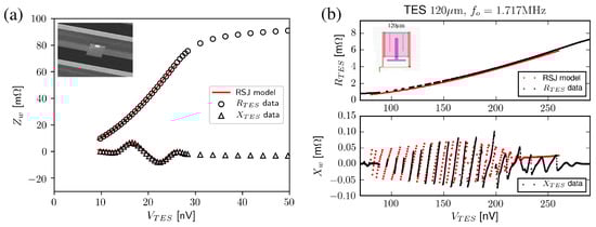
Figure 4.
TES resistance and reactance as a function of the TES voltage for (a) a bare Ti/Au TES bolometer [61] and (b) a NASA-GSFC TES microcalorimeters. The detectors are biased, respectively, at 2.4 and 1.7 MHz. The red lines show the prediction from the RSJ model. Reprinted from [64] by permission from IEEE, IEEE Transactions on Applied Superconductivity. Copyright ©2018, IEEE.
Using a similar approach, but then solving the equations numerically, the peculiar structures observed in the TES reactance of a low resistance (), Mo/Au TES microcalorimeters with noise mitigation structures developed at NASA-GSFC, have been explained as well [64]. An example of the results presented in [64] is reproduced in figure Figure 4b, where the TES electrical impedance is shown as a function of bias voltage. The sharp jumps in the TES reactance , are related to the Josephson effects in combination with a large TES bias current (detector with high saturation power) and low as predicted in [65].
Numerical simulations of the resistive transition of a dc biased TES, based on the RSJ model, have been performed by Smith et al. [34]. The work includes an extensive study on the effect of (self-)magnetic field perpendicular to the TES surface.
The coupled differential equations in Equation (18) have been fully solved numerically, for an ac biased pixel, in the simplified single-thermal body case [66]. In the numerical simulations, the TES impedance is the results of the solution of the RSJ equation and the power balance, as for the analytical solution described in [61]. Aside from the electric circuit and thermal bath parameters, and the TES normal resistance , the most important input for the calculation is the curve, which can be evaluated experimentally. The equilibrium value of the simulated TES current has been shown to be in excellent agreement with the experimental IV curve of the modeled pixel. The strength of this numerical time-domain model is that, beside predicting the steady state of the TES, it can also be used to simulate the TES response to the incoming photons in the non-linear and large signal regime. As a matter of fact, this TES simulator will become part of the end-to-end (e2e) simulator of the X-IFU on Athena [67,68]. In Figure 5, we give an example of the simulation of high normal resistance TES microcalorimeters developed at NASA-GSFC for the Athena/X-IFU and characterized at SRON under MHz bias. The devices consist of Mo/Au bare TESs, with a normal resistance , a and a saturation power at . They have been characterized under ac-bias at several bias frequencies (from 1.1 up to 4.7 MHz). The color maps in Figure 5a,b show, respectively, the TES resistance and reactance as a function of the current I and temperature for a TES biased at . The red curve gives the bias trajectory as the solution of the power balance equation. The TES impedance has been calculated analytically as in [61,62]. A set of curves calculated at a constant TES current are given in Figure 5c. The oscillating structures observed experimentally with this type of TESs are clearly visible on each line as well as on the resulting bias curve in red. The oscillation are generally much smaller when the TES is biased at lower frequency, following the prediction from the Josephson equations.
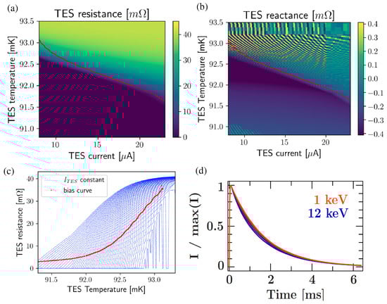
Figure 5.
Colormaps of the TES resistance (a) and reactance (b) calculated for an NASA-GSFC TES microcalorimeters biased at . (c) curves calculated at a constant TES current. (d) Simulated X-ray pulses from photons of energy from 1–10 keV, for a TES biased at 1 MHz at , credits C. Kirsch, 2019.
The curve calculated from the RSJ model can be used as input for the end-to-end simulator under development for Athena/X-IFU to provide a realistic response of the detector to photon of different energy. An example of the simulated X-ray pulses from photons of energy from 1–12 keV, for a TES biased at 1 MHz at is given in Figure 5d. Solving numerically the full equations (Equation (18)) is rather fast [66]. When the calculations are supported by the graphical process units (GPUs), the simulations of an array of 3000 pixels can be done within several hours [68]. The preliminary comparison with the experimental data are very promising [66] and work is in progress to further validate the simulator and to better understand the energy scale of real TES X-ray calorimeter. When the full noise contributions will be integrated, the end-to-end simulator will become a very powerful tool to assist the detectors development for other TES-based instruments as well.
Another interesting technique to guide the detector development is to use optical photons from a laser source to illuminate the X-ray calorimeter via a coupled optical fiber. Using X-ray microcalorimeter from NASA-GSFC, with energy resolution of 0.7–2.3 eV at 1–6 keV, F. Jaeckel et al. [69] have achieved photon number resolution for 405 nm photon pulses with mean photon number up to 130 (corresponding to 400 eV). The experimental set-up is currently being improved to minimize the thermal crosstalk and improve on the photon counting capability to higher energy [70]. This technique is very promising and relatively simple to implement as a standard, inexpensive, calibration facility in a laboratory. In combination with the e2e simulator discussed above, it could become a very useful tool to verify the small and large signal TES response, as well as to understand the effect of the detectors non-linearity on the energy calibration.
2.3. TES Noise
The total noise of a TES detector is a combination of Nyquist–Johnson noise associated with the TES resistance itself and with the losses in the read-out circuit and bias circuit, and thermal fluctuation noise between the TES thermal elements. The noise sources can be classified in external and internal noise sources. Typical external Johnson noise sources are the additive white current noise from the SQUID amplifier and the white voltage noise from the Nyquist–Johnson noise of the shunt resistor in the ac or dc bias circuit. With a proper choice of the parameters of the bias circuit and the SQUID amplifiers, these noise terms can be made negligible. Other external noise sources like, for example, stray light or cosmic photons could generate power fluctuations ( and ) on the detector thermal elements. A careful thermal design of the focal plane assembly can reduce these noise sources to a negligible level.
In Figure 6, we show, as an example, a typical current noise spectra for a Ti/Au TES developed at SRON, ac biased at in the transition at . The different noise contributions are explained here below.
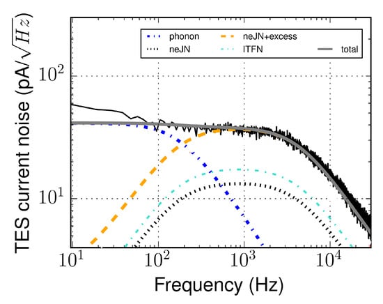
Figure 6.
Current noise spectra of a Ti/Au TES X-ray calorimeter developed at SRON, biased at , at with and [22].
There are three fundamental thermodynamic internal noise sources of a TES detector, described with a two-body model as in Figure 1. The first is the thermal fluctuation noise between the TES detector and the heat bath, already discussed in Section 2. It is prominent in the detector thermal bandwidth typically below . It has a white thermal noise given by , where , as discussed in Section 2, and is a parameter introduced ad-hoc to account for the excess noise observed in the experiments. In the literature, this noise term is typically referred to as phonon or thermal fluctuation noise [14]. The noise contribution to the thermal fluctuation noise from the conductance is generally neglected since . The second fundamental noise term is the so called internal fluctuation thermal noise (ITFN), which is generated by thermal fluctuations between distributed heat capacity (C and of Figure 1b) internal to the TES-absorber system. It has a spectral density , where is the intrinsic thermal conductance. The presence of internal thermal fluctuation noise in TES microcalorimeter was first reported by Hoevers et al. [71]. The origin of the thermal conductance can be of different physical nature depending on the specific TES design. In TES bolometers, for example, the parasitic conductances and the distributed heat capacities is typically attributed to the electrical leads patterned onto the thermally isolating nitride legs [72] or to the SiN legs themselves [73]. In Takei et al. [50], the observed dangling heat capacity arose likely from the thin SiN membrane supporting the low C TES calorimeter. In Goldie et al. [53], the internal thermal fluctuation noise is assumed to be generated by a poor thermal conductance of the TES bilayer and was estimated from the Wiedeman–Franz relationship , where is the Lorenz number. Wakeham et al. [54] investigated the contribution of the internal thermal fluctuation noise on TES microcalorimeters with different design and the origin of the finite term was thoroughly discussed. It can be demonstrated that when passing through the power-to-current transfer function of the electro-thermal system (see for example [52]), the ITFN contribution to the current noise has a shape similar to the Nyquist–Johnson noise described here below, and it is the highest in the kHz range.
The third intrinsic noise contribution is the Nyquist–Johnson noise of the TES itself biased in the transition and it is generalized in the form of a voltage noise . The response of the TES current to is suppressed at low frequency by the electro-thermal feedback [19] and becomes significant in the detector electrical band at kHz. The function , introduced in Equation (2), accounts for the non-linear and non-equilibrium nature of the TES resistance, which is strongly dependent on the TES current. For linear resistors at equilibrium . Irwin [18] assumed the TES to be a simple Markovian system with no hidden variables such as internal temperature gradients and fluctuating current paths. Applying the Stratonovich’s nonequilibrium Markovian fluctuation–dissipation relations, he calculated the first order, near-equilibrium, non-linear correction term to the noise to be . A solution for the higher order terms cannot be found from known TES properties since they contain dissipationally indeterminable parameters [18]. In this form, the noise model is known in the literature as non-equilibrium Johnson noise (neJN) and is extensively used to model the, dependent, Nyquist–Johnson voltage noise observed in the TES. The broadband unexplained or excess noise, typically observed at frequencies larger than the thermal bandwidth of the TES [74], could only partially be explained after the introduction of the correction term and only at relatively low values [34,50,75]. As shown in [52,54,76], the characterization of the noise in the electrical bandwidth is complicated by the fact that both the non-equilibrium Johnson noise and the internal thermal fluctuation noise give a similar contribution in the measured TES current noise, after passing through the system transadmittance. Smith et al. [34], however, excluded the presence of a significant contribution of the ITFN in the excess noise observed with their low resistance, large , high thermal conductance devices.
Noise mitigation normal metal bars and stripes have been proposed and successfully, widely introduced in the TES design of microcalorimeters to suppress the excess noise [74,75].
Kozorezov et al. [77] argued that the observed excess Johnson noise in TES-based detectors could have a natural explanation within the RSJ theory. Following the work of Likharev and Semenov [78], they calculated the power spectral density of the voltage fluctuations across the TES (considered as a resistively shunted junction) , averaged over the period of the Josephson oscillations. They obtained
where are the components of the impedance matrix of the biased TES with the index m standing for the harmonic of the Josephson oscillation at . This approach was used in [79] to develop the quantum-noise theory of a resistively shunted Josephson junction and it was proved that, to calculate the total low frequency voltage fluctuations, one needs to take into account the mixing down of high harmonics of the Josephson frequency. In [77], it was shown that the spectral density of voltage noise in the RSJ model has a unique analytical structure that cannot be reduced to the expression for the neJN from [18] and that the only source of noise is the equilibrium Johnson normal current noise [78]. Moreover, the RSJ model predicts a significant excess noise, with respect to the neJN, for the lower part of the resistive transition, as generally observed in many experiments. In a recent review [80] on the models for the excess Johnson noise in TESs, the authors derived a simpler expression for Equation (20) based on the approximations explained in [77]. They got a voltage noise:
where the in Equation (20) is replaced by R, given the fact that the thermal fluctuations are associated with the real part of the TES impedance at the equilibrium value. In the same paper, they compare the measured Johnson noise for a few TES microcalorimeters [76] with the prediction Equation (21) and the general form derived by Kogan and Nagaev [81] (KN) and the prediction from the two-fluid model [37,80]. In the simplified form of the two-fluid model, no noise is mixed-down from the Josephson to low frequency, and the expected noise is typically underestimated. A better agreement with the data is observed with the RSJ and the Kogan–Nagaev models. In a recent study [82] on the noise of high-aspect ratio TESs under development at SRON for the MHz bias read-out, a very good agreement between the observed Johnson noise and the prediction from the RSJ and Kogan–Nagaev has been demonstrated over a large number of TES designs and bias conditions.
3. Large Arrays Fabrication
A TES is in essence a superconducting metal slice deposited on a substrate. The earliest TES, fabricated in 1941, was just a thin film of lead evaporated onto a 1.5 cm × 1 mm glass ribbon [83]. A TES-based X-ray microcalorimeter fabricated nowadays is more complex and consists of three key components: a temperature sensing element (the TES), a thermal isolation structure, and an X-ray absorbing layer. In this section, we will briefly review these components from the aspect of fabrication including materials and microstructures with the emphasis on the technical scalability. An array of thousands of TESs, realized on a single 4-inch silicon wafer, are under fabrication for the X-IFU onboard of Athena [2] (Section 6.1). Moreover, as it will be reported in Section 6.2, beyond the 2040s, arrays of hundred of thousands of TESs will be required for very large X-ray observatories like, for example, the proposed Lynx space mission [84] or the Cosmic Web Explorer [85]. In parallel to these space missions, increasing the size of the array is also mandatory for many other ground-based applications (Section 6.3). We will discuss here the technical challenges and solutions required to make these large scale arrays a reality.
3.1. TES Bilayer
The TES itself is the core of an X-ray calorimeter. It is the sensing element that can detect very small temperature changes. As shown in Figure 7, it consists of a superconducting thin film connected between superconducting leads. For high resolution spectroscopy, the transition temperature of the film is chosen typically within the range from 50 to 100 mK. However, other transition temperatures can be selected depending on applications. Various types of films have been proposed and successfully used for almost any photon wavelength to achieve the targeted transition temperatures; a single layer of tungsten [86,87], alloys such as Al-Mn [88], and proximity-coupled bilayers (or multilayers) of Ti/Au [89], Mo/Au [90,91,92,93], Mo/Cu [94], Ir/Au [95], and Al/Ti [96,97]. The geometric size of the superconducting slices is normally tens of microns or larger so wet etch, dry etch, or lift-off processes can be adopted in combination with a standard UV photolithography.
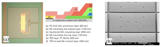
Figure 7.
(a) Microphotograph of a 100 × 30 μm Ti/Au TES connected to the Nb superconducting leads and a schematic of a cutting view along with the dotted line. The separated leads are overlapped near the TES film but electrically separated with an oxide insulating layer, forming a microstripline. The figure was reprinted from [89] by permission from Springer Nature. Copyright ©2019, Springer Science Business Media. (b) Microphotograph of an Au X-ray absorber. The absorber is an overhanging structure supported by several stems that can be seen as dots on top of the absorber surface. The two of them located close to the center of the absorbers are thermally connected to the TES thermometer, not visible in the photo.
The materials for the superconducting leads must have a higher transition temperature and a critical current with respect to the TES film. Niobium is widely used, but other superconductors such as niobium nitride, molybdenum, and aluminum are also applied. One of the technical challenges for the scalability of the sensing structures is the topology of the wirings on a detector chip. Superconducting broad-side coupled micro-striplines are essential in creating dense-packed arrays. An example of the structure of the microstripline is given in the schematic of Figure 7a. It consists of two layers of the superconducting leads, which are electrically isolated by a thin oxide layer. The state-of-the-art system of wiring lines consists of multiple broad-side coupled lines, embedded within oxide layers by applying chemical mechanical polishing so that planarized microstripline layers can be stacked in a vertical direction. Massachusetts Institute of Technology Lincoln Laboratory has demonstrated the process with six superconducting Nb layers for superconducting electronics [98,99,100].
3.2. Thermal Coupling to the Bath
A TES film kept at its transition temperature by the electro-thermal feedback, must be weakly connected to the thermal bath stabilized at a temperature . The thermal link must be properly engineered to be in accordance with the application requirements. A low-stress, silicon-rich membrane is widely used, with a few exceptions, to achieve the thermal isolation because it is mechanically strong and compatible with the other processes used in TES fabrication. The thermal conductance can be controlled by changing the thickness of the membrane and its geometric design, by introducing, for example, slit holes or other phonon scattering structures. In Figure 8a, we show a photograph of an array of ultra-low-noise TES bolometers suspended with 4 diagonal thin and long legs with dimensions [101], giving a good example of how the SiN membrane is mechanically stable and flexible in its design. For X-ray calorimeters, the membrane has a rather simple squared geometry, typically without etched holes or slots. As an example, Figure 8b shows a microphotograph of thousands of squared pockets vertically etched through the Si carrier wafer of 300 μm by using a deep-Reactive Ion Etching (RIE) process. It is possible, in this way, to create a uniform large array of the 0.5-μm-thick SiN membranes with very high yield. The scalability towards an array of 100-kilo pockets is not considered a bottleneck [102].
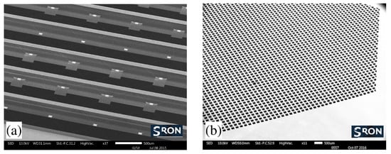
Figure 8.
(a) SEM micrograph of an array of ultra-low-noise TES bolometers on suspended SiN structures with diagonal long legs () design. In the middle of each detector there is a TES and an absorber on a SiN membrane [101]. (b) Microphotograph of an array of thousands of square pockets etched by using a Si deep-RIE process. The pocket size is 190 × 190 μm and the pitch is 250 μm.
A critical issue however remains the proper thermalization of the Si carrier structure to minimize the cross talk between the nearest neighbor pixels located on each pocket. This could become critical when large arrays need to be built. For a k-pixel array under development for X-IFU, it was show that the thermal crosstalk between pixels can be made smaller than (well within the requirements derived from the scientific goals of X-IFU) by coating the back-side and sidewalls of the Si grid structure with a layer of Cu or Au with an appropriate thickness [103].
3.3. Absorbing Layer
An absorbing layer that is thermally well connected to the TES is an essential component of an X-ray microcalorimeter. The absorbers can be directly attached to a small area of the TES slice, or can be place over/near the TES films via thermal coupling structures [94]. For imaging detectors, the absorber is placed directly on top of the TES to maximize the filling factor and hereby defines generally the pixel size. Several absorbers can also be connected to a single TES via thermal links of different length, as it is the case of the emerging class of detectors discussed in Section 5.4.
It is important that the absorber has a high intrinsic thermal conductance to guarantee a fast thermalization, after a photon hit, and to minimize potential internal fluctuation noise. The absorbers are employed to enhance the quantum efficiency of the devices over the target energy band. Thus, providing sufficient stopping power over the large detection area is of primary importance. Therefore, materials of high atomic number with good thermal conductivity are desired. In the soft X-ray field, semi-metals like Bi or normal metal such as Au and Cu have been widely used. In Figure 7b, we show a microphotograph of an X-ray absorber made of a 2.3 μm thick Au film, which provides a quantum efficiency of 83 % for a 6 keV photon. It is possible to achieve a quantum efficiency as close as 100 % by increasing the thickness of Au up to 7 μm at the cost of an increase of the heat capacity and a degradation of the detector sensitivity. To overcome this counter-effect, Bi, which has a very low specific heat at low temperature, can be deposited directly onto a thinner normal metal absorbing layer like Au.
The absorbing layers can be deposited by using sputter deposition, evaporating, or electroplating. Any of these can be adopted to form a uniform large array, but electroplated thin films have been shown to achieve higher Residual-Resistivity Ratio (RRR), usually defined as the ratio of the resistivity of a material at room temperature and at mK, and better thermal characteristics [104,105]. Furthermore, electroplating is preferable, especially for the thicker layers, to minimize the thermal loading during deposition and the stress in the films. On top of this, evaporating thick layers of Au is far too expensive. In Figure 9, we reproduce the scanning electron micrographs of evaporated and electroplated bismuth studied at NIST to better understand the non-Gaussian spectral response observed in X-ray absorbers [105].
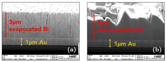
Figure 9.
Scanning electron micrographs of the (a): evap-Bi and (b): elp-Bi absorber cross-sections. The evap-Bi grain appears smaller than that of the elp-Bi, and shows a columnar structure. Reprinted from [105] by permission from AIP Publishing. Copyright ©2017, AIP Publishing.
To achieve the required high QE however, a careful study needs to be performed on the thickness and the quality of the Au/Bi bilayer. It has been recently shown [106] that the roughness, the edge profile, the angles of incident of the X-ray photons, and the filling factor needs to be known well to obtain an accurate estimate of the QE. To minimize the effect of the absorption of the stray light in the detector, it is also desirable to increase the reflectivity of the absorber for long-wavelength infrared radiation. For an Au/Bi absorber, this can be done for example by adding a Au capping layer on top of the Bi, with a thin Ti adhesion layer. A quantum efficiency of 90% has been reported for TES-X-ray calorimeters designed for Athena/X-IFU [106] with an increase of reflectivity, measured at room temperature, from 45% to up to 80% after adding a 40 nm Au capping layer.
In some particle physics experiments that aim to directly detect the neutrino mass using a large array of TES X-ray microcalorimeters (see Section 6.3), a precise amount of radioactive material like Ho, has to be embedded in the detector absorber. A multi-step micro-fabrication process to achieve this is described in [94]. One crucial part of such a process is the co-deposition of gold during the Ho implantation process on the detector absorber.
4. Single Pixel Optimization
In this section, we will review the progress in the pixel optimization for a large array to be used in dc and ac biased multiplexing schemes. Detectors with excellent single pixel energy resolution are shown regularly in many laboratories. The big challenge however remains to find an optimal pixel design and fabrication process that guarantees high yield and uniform performance over a large number of pixels. The underlying physical effects discussed in Section 2 have different implication on the performance of the TESs according to whether the detector is dc or ac biased, as it was reported in several works [34,107,108]. A tailored optimization approach is then required, in view as well of the different applications.
4.1. dc Bias
For many years, the efforts to improve the single pixels performance of TES microcalorimenters have been devoted in trying to suppress the poorly understood excess Johnson noise, typically increasing at larger . It was empirically observed that adding normal metal stripes on top of the TES bilayer would mitigate the overall noise [74,109]. Detectors with very good energy resolution have been fabricated following these finding [15]. With the increasing demand of larger and larger arrays of pixels, it was soon realized that normal metal structures could strongly affect the shape of the resistive transition in a way that it was not always controllable and reproducible. Moreover, kinks in the transition have also been regularly observed with those devices. This is partially due to the fact that the proximity effects discussed in Section 2.1 are strongly dependent on the device geometry, the transmissivity of the leads-TES interface and other parameters of the SNS structures, such as , and coherence length. In a series of very detailed experiments, it was shown, by Smith et al. [34,110] and in later works [76,111], how the normal metal structures added to the TES, including the thermal coupling stems between TES and absorber, could dramatically change the resistive transitions shape and the current flow [112], as a complex interplay of proximity effects, non-equilibrium superconductivity, and self-induced magnetic field. An improved TES design was highly desired, in particular because the dc bias multiplexing schemes do not allow a single pixel bias optimization. Due to the common bias configuration, they require an extremely high uniformity over a large array of pixels.
The traditional strategy of suppressing by adding normal stripes on top of the bilayer has the side effects of reducing as well, since , and were found to be correlated [15,34]. An alternative approach was needed. From Equation (2), it is known that, in the small signal limit, for a given detector and heat capacity C, to achieve the best energy resolution one needs to minimize the factor , which depends on the TES geometry and where generally increases with . In a study on the performance of Mo(50 nm)/Au(200 nm) TESs with different stripes configurations [113], it was shown that pixels without stripes could achieve excellent resolution even with a large non-equilibrium Johnson noise in excess. An excellent energy resolution of at was reported with a small, , bare TES with , coupled to a Bi()/Au() absorber with heat capacity . The stripe-less small device had much larger values of 1600), 86) and 6) with respect to the larger size TESs with stripes (, and ) [114], which showed energy resolution around and were under consideration for X-IFU.
This result was a real breakthrough in the field, because it suggested that the parameter space for the optimization of TES microcalorimeters for ultra sensitive X-ray spectroscopy, could be much larger than what it was thought before. The major advantages of removing the normal metal stripes from the top of the bilayer and of employing small TESs are the smaller sensitivity to the external and self-magnetic field, the improvement of the uniformity of the TES resistive transition itself and an increased uniformity within the array. Excellent uniformity has been demonstrated with a kilo-pixels array of TES X-ray calorimeters under development for X-IFU (Section 6.1). The detector design is based on the small, , Mo/Au bare TES described above. A combined energy resolution of at 5.9 keV, obtained with more than 200 pixels, in a multiplexing configuration, has been reported [115].
Small pitch () devices based on a similar design, fabricated in an array of sensors, with thick, , gold absorbers have been developed at NASA-GSFC for the low energy band (0.2–0.75 keV) of the Ultra High Resolution (UHR) array for the future X-ray space mission Lynx Section 6.2. They measured 2.31 eV FWHM at 1.49 keV, limited by the broadening of the intrinsic linewidth of the Al source, and 0.25 eV FWHM at 3 eV using optical photons, from a blue laser diode, delivered through an optical fiber [69]. The latter energy resolution result is consistent with the estimated performance based on the signal size and noise [116].
4.2. ac Bias
TES microcaloremeters to be read-out under ac bias for the MHz-FDM-based experiments require a different optimization process than the one described above. The uniformity of the transition over a large array is less critical, due to the fact that in FDM each pixel can be biased individually to their optimal point. The performance of MHz biased TES is deteriorated by two major frequency dependent effects: (i) the ac losses from eddy currents generated in the normal metal structures and (ii) the ac Josephson effects describe in Section 2. The former induces thermal dissipations inside the TES and absorber [64,117], which effectively decrease and the detector sensitivity, in particular at high bias frequency and for low resistance bias points where the best signal-to-noise is generally achieved. The latter is responsible for a relatively large non-linear Josephson inductance in parallel with the TES resistance. At high bias frequency, it reduces the range for optimal biasing at low TES resistance and generates step-like structures in the TES transition [64,118,119].
Through an experimental and theoretical study, the groups at SRON and NASA-GSFC have identified several optimal TES designs for the ac-bias read-out. They implemented changes both in the TES geometry and the fabrication process. The ac losses have been minimized to a negligible level by: (a) reducing the Au metal features, like the stripes and the edge banks, in the proximity of the TES and the leads, (b) making the non-microstriped loop area formed by the TES and the bias leads smaller, and (c) increasing the TES aspect ratio (AR = ), where the width (W) is reduced relative to its length (L), to achieve higher value of . Moving towards higher and higher TES normal resistances, has also been the strategy to minimize the Josephson effects in ac bias devices, as it follows from the predictions of the theoretical models presented in Section 2.2. In TESs with higher , operating at the same power, the gauge invariant phase difference across the Josephson weak link is maximized since and the TES is less affected by the Josephson effects. Similarly to the dc bias pixel optimization, a further strategy was to simplify the geometry of the TES by removing additional metal features such as the Au stripes that are responsible for a complex resistive transition. Both these actions are compliant with those also implemented to reduce the ac losses.
The dependence of the Josephson effect on TES power P, and bias frequency is phenomenologically demonstrated in Figure 10.
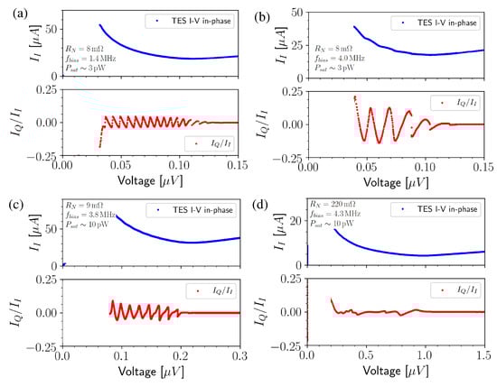
Figure 10.
TES I–V curves for different X-ray microcalorimeter types and MHz bias frequencies. In the lower graph of each plot the ratio of the quadrature or Josephson () and in-phase current is shown. In (a–c), the bias frequency is, respectively, . The detector is an NASA-GSFC Mo/Au bare TES [113,117] with 8–9 and (a,b) and , respectively. In (d), we consider a Ti/Au, , SRON TES [108] with , , and biased at frequency . Reprinted from [119] by permission from Springer Nature. Copyright ©2018, Springer Science Business Media.
The ratio of the out-of-phase Josephson current () to the in-phase current is shown as a function of TES voltage for low (Figure 10a–c) and high (d) ohmic devices fabricated, respectively, at NASA-GSFC and SRON. In the top-left and top-right plots, the low power () and low resistance () detectors have been bias at low (1.4 MHz) and high frequency (4.0 MHz). At high bias frequency, the ratio () is increased of more than a factor of 2 at low voltage bias. In the two lower graphs, the detectors operates at a high saturation power () and similar bias frequency (). The two TESs have, respectively, and . The high ohmic, high power detectors show almost negligible Josephson effects even at high bias frequency.
There are two ways to fabricate devices with high . One is to increase the bilayer sheet resistance , by reducing the thickness of the normal metal film (Au). Despite the good results achieved in squared TESs even after increasing the from 15 to 50 [54], this approach is not scalable due to limitation in the fabrication process and, eventually, to the increase of the internal thermal fluctuation noise. A better way to achieve high is to increase the TES aspect ratio, defined as AR = , with L and W the TES length and width, respectively. Higher aspect ratio devices, while increasing , offer additional design flexibility to simultaneously reduce the speed of the pixel (by reducing the perimeter) and the TES bias current (at the same saturation power) measured by the SQUID amplifier. Both the effects are beneficial to increase the multiplexing factor, as discussed in Section 5.2.
After a few promising results obtained at NASA-GSFC, SRON developed high aspect ratio TES microcalorimeters based on Ti(35 nm)/Au(200 nm) bilayer with a . In Figure 11, we give an example of the mitigation of the Josephson effects achievable by using high aspect ratio (AR) TESs. From left to right, we show the I–V curves and the ratio of, respectively, an NASA-GSFC Mo/Au (AR = 4:1, ), an SRON Ti/Au (AR = 4:1, ) [22], and an SRON Ti/Au (AR = 8:1, ). All the devices have a 1–2 , compatible with the X-IFU requirement. The NASA-GSFC device is biased at , while for the SRON devices, I–V curves for pixels biased at different frequencies (from 1.5 to ) are shown.
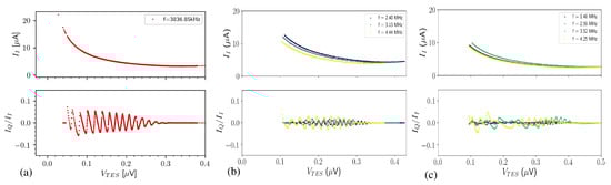
Figure 11.
TES I–V curves for different X-ray microcalorimeter types and MHz bias frequencies. In the lower graph of each plot the ratio of the quadrature or Josephson () and in-phase current is shown. The data are from the following devices: (a) NASA-GSFC Mo/Au (AR = 4:1, ), ac biased at 3.8 MHz, (b) SRON Ti/Au (AR = 4:1, ) [22], ac biased at 2.4–4.4 MHz and (c) SRON Ti/Au (AR = 8:1, , ac biased at 1.4–4 MHz) [22].
The SRON turns out to be very promising, with a , at , smaller than the other devices biased at the same frequency. Although the weak-link effects are not completely eliminated, these new TES design configuration reduces the size of the oscillatory structures in the transition and allows the access to a wider range of higher signal-to-noise ratio bias points in the transition.
We have to experimentally investigate the performance, under ac bias, of many high aspect ratio devices fabricated at SRON with high () [120], and low () [22] critical temperature. The energy resolution was shown to scale with as expected. Five different TES designs with low were then further studied. The geometry of these devices is rectangular with dimensions (length× width) , , , , and , which correspond to aspect ratios ranging from 2:1 up to 6:1. The results on the characterization and uniformity of a kilo-pixels array of is reported in [121,122]. More details on the TES design and fabrication are given in [89] and in Section 3. The TES bilayer had a and a squared normal resistance of . The scaling of the devices and the thermal conductance with the TES geometry has been studied carefully. It is shown that the is decreasing with increasing TES length and decreasing width, in agreement with the LaiPE and LoPE models described in [21]. The thermal conductance, evaluated at the critical temperature, was shown to scale with the perimeter of the device, as expected when the dominant process for the thermal conductance is two-dimensional radiative transport in the silicon nitride membrane [123,124]. The thermal characterization of the devices is essential for the development of large uniform arrays tailored for the multiplexing read-out and the instrument requirements. The devices showed excellent energy resolution at , with a mean of and median of 2.07 eV over all the tested geometries and bias frequencies from 1 to 4 MHz [22]. The best results were obtained with the , with AR = 6:1, with energy resolution consistently below 2 eV. These results show that, even with high aspect ratio and very high normal resistance devices, there appears to be no degradation in the performance and in the signal-to-noise ratio. This seems to indicate that the internal thermal fluctuation noise, for example, do not simply scale with the TES normal resistance.
The good results have motivated the team to explore the performance of extreme aspect ration TESs and more exotic geometries, given the assumption that the Josephson effects should be minimized in high normal resistance devices. Devices based on TiAu TESs have been fabricated at SRON with aspect ratio as high as AR = 15:1, including TES with small width and meandering geometries. The characterization of these new devices is currently on going, but the first results are very promising. In Figure 12, we show the energy spectrum at 5.9 keV of and Ti(33)Au(210) TESs with, respectively, ∼ 65 and , optimized for the MHz frequency-division multiplexing readout of X-IFU-like instruments. The of these TESs is ∼86.5, and they are both coupled to a Au () absorber with a total heat capacity of at . Excellent energy resolution at 5.9 keV has been achieved. An example is given with the two spectra in Figure 12 taken at about . An energy resolution of and , has been achieved, respectively, with the TES biased at and the TES biased at . The spectra are the result of many hours of acquisition at a count-rate of about 0.8–1 pulse/s. They have been taken with the set-up described in [22] hosted in a shared facility where two other experiments were running simultaneously. Multiplexing demonstrations for X-IFU-like X-ray instruments are currently being done with SRON and uniform array of the high aspect ratio devices discussed above. As it will be shown in Section 5.2, the first results are very encouraging. It is likely that a further improvement in the energy resolution and multiplexing performance will be shown in the near future with the new generation of TESs.
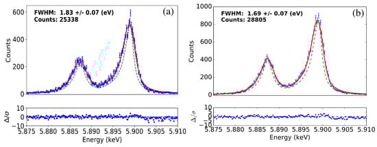
Figure 12.
X-ray spectra of the Fe complex at 5.9 keV demonstrating excellent energy resolution with SRON high aspect ratio TESs: (a) , and bias frequency 2.5 MHz, and (b) , and bias frequency 3.5 MHz. The dashed green line is the natural lineshape of the complex.
5. Multiplexing Readout
Large arrays with thousands of pixels are nowadays routinely fabricated and the demand from future experiments is to scale to higher number of pixels, towards the ambitious target of 100 kilo-pixels or more. A further improvement of the existing cryogenic multiplexing read-out technology is a must, to reduce the dissipation from the SQUID amplifiers, the readout, and bias wiring, and to minimize the size of the interconnections and the harness complexity. It is not our purpose to discuss the details of the existing cryogenic multiplexing systems, which have been well reviewed in [15]. In this section, we will give a short overview of the state-of-the-art of the different multiplexing readouts. SQUID-based multiplexing techniques for TES bolometers and micro-calorimeters have been developed and operated at MHz frequencies using only few of the many orthogonal basis sets conceivable [12], such as time-division multiplexing (TDM) [9,125], MHz frequency-division multiplexing (MHz-FDM) [12,126,127], and Walsh code-division multiplexing (CDM) [10,125,128]. The state-of-the-art of each of these techniques is currently limited by the practical implementation. The resources required by multiplexed signals will be independent of the applied basis set, when optimally dimensioned and with full signal loading. The choice of which multiplexing readout to use should be then based on the specific system requirements, such as, for example, cooling power, mass, volume, harness length, and electromagnetic interferences compliance.
Microwave frequencies multiplexing schemes (GHz-FDM), using microwave SQUID multiplexing (μμw-mux), is becoming a mature technology both for transition-edge sensors [11,129] and magnetic microcalorimeters [130], in particular for ground- base applications.
The number of pixels presently multiplexed in each multiplexing scheme is far below the fundamental limit set by the the information theory [131]. This is partially due to the fact that the cryogenic environment and the lithographic fabrication set stringent constrains that make it difficult to optimally implement any multiplexing architectures. Much R&D is still needed towards the optimization of the practical implementation of the multiplexing schemes in the focal-plane design to accommodate the complex cryogenic electronics. It is likely that for multiplexing a 100,000-pixels array, a hybrid multiplexing configuration will be required [132].
5.1. Time-Division and Code-Division Multiplexing
SQUID-based time-division multiplexing (TDM) is, at the moment, the most mature technology to read-out arrays of TES microcalorimeters. In TDM, the TESs are dc-biased. Each TES is coupled to its own first-stage SQUID. N rows of first-stage SQUIDs are switched on sequentially and M columns of SQUIDs are read out in parallel. One single bias line is used for all the N TESs in one column and each TES cannot be individually biased at its optimal bias point. For this reason, a highly uniform TES array is required.
The latest generation of TDM architecture developed at NIST has an overall system bandwidth of bandwidth, which allows to switch the rows faster with transient of and total row time of . A three-stage SQUID configuration is used with a input flux noise of . More details of the state-of-the-art of the TDM architecture, including the description of a practical X-ray spectrometer for beamline science, can be found in [9,133]. Recent 40-row TDM experiments with X-IFU-like TESs make use of new shunt resistors and the optimized first-stage SQUIDs recently developed at NIST [125]. The achieved 1x40-row (32 TES rows + 8 repeats of the last row) energy resolution with the 32 TESs was at 1.5 keV, at 5.9 keV, at 6.9 keV, and at 11.9 keV [128]. A NIST 8-columns×32-row TDM system with a prototype of a X-IFU kilo-pixel array from NASA-GSFC has shown an exquisite average energy resolution of at 6.9 keV [134]. The instrument will be soon delivered to LNLN EBIT for astrophysics experiments. These results are compliant with the stringent Athena X-IFU requirements.
The main disadvantage of TDM is the increase of SQUID noise with the due to aliasing, into the signal bandwidth, of the Nyquist noise above the rate at which all the N pixels in a column are measured and below the measurement bandwidth. This sets a fundamental limit on the maximum number of pixels measurable with high resolution in multiplexing mode. Code Division Multiplexing (CDM) [135] provides a way to reduce at a negligible level the SQUID noise aliasing effect and has the big advantage of being compatible with the existing TDM read-out infrastructure. In CDM, rather than measuring one TES at a time, all the dc-biased TESs in a column are read out simultaneously at each time step. The signals from the TESs are encoded with a Walsh basis and summed with equal weight, but different polarity patterns. The design and fabrication of the SQUID multiplexing chip is rather complex, since the encoding is achieved by a flux-summing architecture of N different microcalorimeters in N different SQUIDs with different combinations of coupling polarity. CDM is also susceptible to single-point failure mechanisms which can result in an unconstrained demodulation matrix. However, potential solutions do exist [136]. Excellent performance has been reported so far with a 32-channel flux-summed CDM [10] with a mean energy resolution of over 30 working sensors. The multiplexed noise level and signal slew rate achieved were sufficient to allow the readout of more than 40 pixels per column. Even a larger multiplexing number could be achieved with the recent technological improvement in the fabrication of the shunt resistors chip and the first-stage SQUIDs [125].
5.2. MHz-Frequency-Division Multiplexing
The MHz Frequency-division multiplexing (MHz-FDM) scheme is fundamentally different from the other multiplexing architectures from the fact that the TES itself, and not the SQUID, is the modulating element in the multiplexing process. The detectors are voltage biased with sinusoidal carriers at different frequencies in the 1 to 5 MHz range and they operate as amplitude modulators [137]. MHz-FDM is under development for the read-out of large array of X-ray calorimeters and infra-red bolometers for future space mission and used on ground-based CMB experiments [138,139]. In MHz-FDM, each TES is coupled to a superconducting high-Q bandpass filter [55,56,140,141], which has the double function of limiting the information bandwidth and providing a single carrier, stiff ac voltage bias to the TES. The signals from many TESs are then summed at the input of one low-temperature first-stage single SQUID current amplifier, amplified further by a second-stage SQUID array, operated at higher temperature, and finally demodulated at room temperature by digital electronics. The SQUID signal is linearized by using a very robust baseband feedback (BBFB) scheme [57,142,143] or other digital active nulling configuration [144]. The major advantage of the MHz-FDM architecture is the relative simplicity of the cold electronics, which only requires a limited amount of SQUID amplifiers, and its robustness to electromagnetic interferences. The fabrication of high-Q lithographic filters has been, for many years, a major obstacle to the practical implementation of the MHz-FDM. With the state-of-the-art of the -filters fabrication, a very high yield can be achieved, as well as a high accuracy of the frequency definition and a compact design [55]. FDM makes as well a better use of the available bandwidth with respect to the other traditional scheme.
Moreover, in an instrument like X-IFU for example, tens of pixels can be readout with a single SQUID amplifier, without the need of more dynamic range than for the readout of a single pixel [145]. The details of the MHz-FDM system for a X-IFU-like instrument, using for each channel a two-stage SQUID amplifier developed at VTT [146], can be found in [12]. The first-stage SQUID has an input inductance smaller than , a bandwidth and a input current noise , for a total power dissipation smaller than .
One of the major issues related to the MHz-FDM readout is the behaviour of a TES under MHz bias, which is strongly influenced by the non-linear Josephson effects describe in Section 2. Only recently, the physical processes involved in an ac bias TES have been better understood. The current development undergoing at SRON (see Section 4.2) is leading to an optimal TES design that will reduce these non-ideal effects to a negligible level.
Moreover, non-linearities in the readout chain, due to, for example, the SQUID amplifiers or DACs, can generate intermodulation lines within the detector bandwidth degrading its performance. To minimize the effect of these non-linearities and to make efficient use of the available readout bandwidth, the LC resonators are usually designed to be on a regular grid. Despite the high accuracy of the lithographic processes, however, the observed resonant frequencies have a spread of about few kHz around the designed values. The important recent breakthrough that solves this issue is the experimental demonstration at SRON of the frequency shift algorithm (FSA), a very elegant approach to electronically tune the resonant frequency of the cold resonators by means of a feedback on the modulated bias signal [147]. The performance of a new implementation of the FSA, scalable for multi-pixel operation, has been recently shown by Vaccaro et al. [126]. An energy resolution of at 5.9 keV has been achieved in a summed energy spectrum with 20 pixels, from a 5 × 5 array of Ti/Au TESs microcalorimeters with an intrinsic single pixel energy resolution of about 2.7 eV. A new experiment has been performed with a larger filters array and using an uniform array of X-IFU-like TESs with a measured single pixel energy resolution of ∼1.8 (see Figure 12). An excellent energy resolution of at 5.9 keV has been demonstrated with 32 pixels multiplexed [148]. At the time of writing this review, a at 5.9 keV has been demonstrated with 37 high aspect ratio pixels, with geometry , in a k-pixels array multiplexed at frequencies from 1 to 5 MHz [149]. The results fulfill the X-IFU requirements. This is the first convincing demonstration of MHz-frequency division multiplexing with TES microcalorimeters. Improvements are still expected in the coming years, after a fine tuning of the read-out circuit and when employing further optimized detectors currently under fabrication. These recent results show no fundamental limitation yet for this multiplexing scheme. The MHz-FDM is reaching a competitive level of maturity, and has the potential to achieve even higher multiplexing capability per SQUID channel. As a matter of fact, the current implementation of the current MHz-FDM is far from optimal and increasing the the bandwidth to 6 MHz appears to be feasible. Many new ideas have still to be implemented to efficiently use, for example, the limited resources available for space-borne instrumentations [145,150,151].
5.3. GHz-Frequency-Division Multiplexing
The multiplexing architectures discussed so far do have a limited ultimate bandwidth around 10 MHz. SQUID-based microwave read-out is a promising technology under development to expand the read-out bandwidth to the GHz range. The large bandwidth available can be used to multiplex a larger number of TESs or to allow more read-out bandwidth per pixel. A microwave SQUID multiplexer (μw-mux) performs frequency division multiplexing at GHz (GHz-FDM). Differently from the MHz-FDM, the TESs are dc-biased and rf-SQUIDs are used to modulate distinct superconducting microwave resonators coupled to a common microwave feed-line [11,152,153]. The signal of thousand of pixels could finally be amplified at 4K by standard HEMT amplifiers in the, 4- to 8-GHz band, via a single coax cable. Despite the complexity at many levels of the signal chain, as for example the design and fabrication of the cold rf-SQUID and resonators chips [154], the linearization of the SQUID response [11,155], the room temperature electronics, and the packaging at the focal plane assembly stage, the GHz-FDM will become very competitive in the future. This is particularly true for ground-based experiments and in applications where a large array of high speed detectors are required [130,156]. The SLEDGEHAMMER instrument with gamma-ray detectors, has demonstrated the read-out of 128 microwave SQUID multiplexed channels on a single set of coaxial cables [11]. With a similar set-up, a 82 pixels multiplexing factor has been demonstrated on an array of soft X-ray TESs with an energy resolution of for the magnesium K line at 1.25 keV, consistent with the resolution achieved using TDM with the same array [129]. A simultaneous readout of 38 high-ohmic Ti/Au SRON TES microcalorimeters has been recently demonstrated with a low noise μw-mux SQUID amplifier fabricated at AIST in Japan. With a readout noise of , a median energy resolution of 3.3 eV at has been achieved [157] with high normal resistance and relatively fast detectors. The multiplexing factor achievable with microwave SQUIDs is limited by the bandwidth available in the HEMT amplifiers (currently only working between 4–8 GHz) and the high slew rate on the leading edge of X-ray pulses. For the latter, workarounds are envisioned [158].
5.4. Thermal Multiplexing
The maturity level of the electrical multiplexing architecture discussed above is such that in the next decade they will become a standard technology in the read out of array of few thousand pixels. Scaling up this technology for the multiplexing of arrays of 100,000 pixels or more will become prohibitive, if only to electrically connect all the pixels on the wafer. Multiabsorber TESs [159], also commonly referred to as ‘hydras’, for the peculiar shape of these devices, are an alternative approach to increase the multiplexed number of pixels without a dramatic increase in the number of readout components. The principle behind the hydra is to couple to a single TES a series of many absorbers, such that each of them acts as a separate imaging element or pixel. The thermal link between each of the absorbers to the TES is engineered such that it has a slightly different thermal conductance. In this way, the TES measures a different temperature excursion for photon hits in the different absorber. The information of which pixel received the photon can be retrieved from the pulse shape recorded by the electronics. The Hydras concept and implementation has been pioneered by the NASA-GSFC team and the most up-to-date theoretical and experimental results have been reported by Smith et al. [115,159]. An intrinsic trade-off between energy resolution and position sensitivity does exist for hydras detectors. It depends upon the ratio of the internal thermal conductances between absorbers to the external thermal conductance to the bath. In addition, the maximum number of thermally multiplexed absorbers is limited by the ability of the pulse processing algorithm of discriminating the different pulse shapes, which is related to the electrical bandwidth available to readout the coupled TES. With no doubt, the hydras will become an essential element of the future hybrid multiplexing architectures required to read out very large arrays of TES microcalorimeters.
6. Future Instruments for Astrophysics and Fundamental Physics Research
The current performance of X-ray TES-microcalorimeters and their multiplexing read-out have reached a level of technological maturity to be employed as baseline detectors at, for example, synchrotron and free electron laser facilities as very sensitive, science driven, X-ray spectrometers. Those instrument has been reviewed in [15] and will not be discussed here.
In this section, we will focus on the development of TES-based instruments for astrophysics space telescopes and fundamental physics experiments. The state-of-the-art detectors and the ultimate sensitivity is generally required for most of these future ground-breaking scientific experiments.
6.1. X-IFU Athena
One of the most complex TES-based instruments currently under development is the X-ray Integral Field Units (X-IFU) of Athena [16], the L-class ESA’s X-ray observatory mission, selected in June 2014 to address the Hot and Energetic Universe science theme [2] and scheduled to be launched on 2032 at L2 orbit. The Hot Universe refers to the baryons at temperatures above , which are believed to account for half of the total baryonic content of the Universe. The best observational handle on the energetic universe is through X-ray observations of hot gas and accretion around black holes. Athena will be a large observatory offering an unprecedented combination of sensitive X-ray imaging, timing, and high-resolution spectroscopy. X-IFU [2] is a cryogenic imaging X-ray spectrometer, with spatially-resolved high spectra resolution over a field-of-view (FoV) that will provide: (i) 3D integral filed spectroscopic mapping of hot cosmic plasma, (ii) weak spectroscopic line detection, (iii) physical characterization of the hot and energetic universe. X-IFU will host an array of more than 3000 TES pixels with a , sensitive in the energy range of 0.2–12 , with an unprecedented instrument energy resolution of 2.5 eV at 7 keV. To achieve the X-IFU requirement, the intrinsic single pixel energy resolution has to be better than 2 eV, the quantum efficiency of the absorber at , respectively, and pixel filling factor larger than 0.97.
The prototype kilo pixel array of Mo/Au TESs, developed at NASA-GSFC and read out with the 8-column by 32-row TDM from NIST, has recently shown excellent results that meet the X-IFU requirement with margin. The detector consists of an array of , low resistance TESs with a single pixel resolution of <2 at . The system has demonstrated a combined exquisite energy resolution, with more than 200 pixels, of: 1.95 eV for Ti-K (4.5 keV), 1.97 eV for Mn-K (5.9 keV), 2.16 eV for Co-K (6.9 keV), 2.33 eV for Cu-K (8 keV), 3.26 eV for Br-K (11.9 keV) [115]. The focus of the team will soon move on demonstrating the performance of a full scale pixels array. Thanks to its advanced readiness level, this technology is currently baselined for X-IFU for the mission adoption of Athena expected in 2022.
The X-IFU Focal Plane Assembly (FPA) [160,161,162] and the detection chain shall face several implementation challenges related to the interaction between the different components of the read-out (i.e., the main sensor array, the old electronics stages and the warm electronics) and the thermal, mechanical, and electromagnetic environment. Moreover, the limited resources available on the space telescopes lead to strong constrain on the total allowed mass, volume, electrical power, and cooling power at the and stages.
The high-frequency EM-fields generated in the spacecraft call for a careful choice of the read-out technology that needs to be the less sensitive to electromagnetic interferences and capable of driving very long cable harness. The high susceptibility of the TES detectors and the focal plane assembly to DC and low frequency magnetic fields requires a proper magnetic shielding, by means of -metal and Nb shields, to reduce the DC and the B-field to level with a stability ∼10 . Faraday cages needs to be implemented at the FPA, warm electronics, and cryostat level and the harness needs to be heavily filtered given the high (∼0.4 ) susceptibility in the DC-MHz range [161]. In Figure 13a, we show a rendered view of the FPA Demonstration Model of X-IFU, currently in the commissioning phase at SRON. On the right side of the figure, we show the pictures of a full scale X-IFU prototype array from NASA-GSFC with more than 3000 pixels on a pitch of . The focal plane assembly should also be designed to minimize the infra-red and optical loading on the TES. This should be achieved by thermal filters in the aperture [163] and Au shielding in the proximity of the array. On top of that, the energy resolution of the detectors can be affected by thermal bath fluctuations from the energy deposited on the substrate by cosmic rays from astrophysical sources [164,165] and by micro-vibrations induced by the mechanical coolers [162,166]. A proper coating and thermalization of the TES array wafer can minimize the impact of the cosmic ray [167], while a sophisticated Kevlar-based suspension system is in development to provide robustness and stiffness to survive the launch and sufficient thermal and mechanical decoupling from the different cryostat stages [162]. Finally, the X-IFU TES array sensitivity will be degraded by the particles background which is induced by primary protons of both solar and cosmic rays origin, and secondary electrons. To prevent that, a Cryogenic AntiCoincidence (CryoAC) detector is placed in the proximity of the X-IFU TES array [168]. The CryoAC is a 4-pixels detector made of wide area silicon absorbers sensed by a network of about 120 IrAu TESs connected in parallel. It is located at a distance of <1 mm underneath the TES-array. A set of low-Z material shields in between the TES array and the Niobium shield will minimize the effect of secondaries. In this configuration, the X-IFU particle background will be reduced to a total level <5 in the 2–10 keV energy band. The first simultaneous operation of a CryoAC prototype developed at INAF, with a NASA-GSFC TES kilo-pixel array read-out in single pixel mode by a MHz-FDM set-up developed at SRON has been recently reported by Macculi et al. [169].
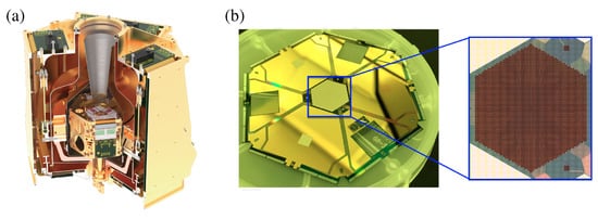
Figure 13.
(a) X-IFU Focal Plane Assembly Demonstration Model. (b) Photograph of a X-IFU prototype array from NASA-GSFC with more than 3000 pixels on a pitch of . Courtesy of the X-IFU FPA team at SRON and NASA-GSFC.
6.2. Other Future X-ray Space Missions
After the European mission Athena, other X-ray observatories are currently being proposed in China, Japan, and USA.
The Hot Universe Baryon Surveyor (HUBS) [170], proposed in China, is designed to explore and characterize the circumgalactic medium with a large FoV. HUBS will be complementary to Athena. Thanks to the larger FoV ( angular resolution pixels over a FoV, while X-IFU has ∼5 pixels over a FoV of equivalent diameter), it is optimized to measure the spatial profile of extended warm-hot gas around galaxies and clusters of galaxies, and, potentially, the filamentary structures in the cosmic web, as well. The array of TES microcalorimeters is designed to have pixels with an area of for each pixel. A central array with smaller pixels is foreseen. The large Au/Bi absorbers required for this mission will be an interesting fabrication and optimization challenge [171]. The X-ray spectrometer will cover an energy range from 0.2–2 with expected energy resolution of and for the outer and inner array, respectively. The multiplexing read-out will be chosen between TDM, MHz-FDM and GHz-FDM depending on the overall system requirement.
Orders of magnitude larger pixels arrays are envisaged for the future proposed large X-ray mission beyond Athena such as Lynx, Super-DIOS, and the Cosmic Web Explorer that will be briefly discussed here below. The Lynx X-ray Observatory [84], is one of four large satellite mission concepts currently being studied by NASA. Lynx will provide a significant increases in sensitivity, FoV with subarcsecond imaging, and spectral resolution over Chandra and Athena. The three main science objectives of Lynx are: (i) the observation of the dawn of black holes, (ii) he understanding of the driving of the galaxy formation and evolutions, (iii) the study of the energetic side of the stellar evolution and the stellar ecosystem. One of the instruments on board of Lynx is an imaging spectrometer composed of a very large array of TES microcalorimeters [102]. To meet all the Lynx requirements, the focal plane array is expected to be divided in different sub-arrays, which will make it unique. Its main array will consist of 86,400, over an area of , with an energy resolution at 0.2–7 . At the innermost central 1 arc-min region, an array of 12,800, smaller, pixels will provide up to . Finally, there will also be an ultra-high resolution subarray, optimized to achieve high energy resolution of under . To read-out such a large array of 100,000 pixels will set a challenge not only for the multiplexing, but for the layout of the wiring on the detector and bias circuit chips as well. NASA-GSFC has developed a process to combine planarized multi-stack buried wiring layers from Massachusetts Institute of Technology Lincoln Laboratory (MIT/LL) [98,99] with their TES array design [115]. It will not remain a dream any more to realize a 100 k pixels instrument for a future space mission, by combining the heritage from X-IFU (Athena), the TES hydras concept discussed in Section 4.1, with the state-of-the-art of GHz-FDM [129], or a hybrid configuration including the traditional multiplexing read-out.
In Japan, ISAS/JAXA is considering the Super Diffuse Intergalactic Oxygen Surveyor (DIOS) space mission [172] for a launch after 2030. The science case is similar to HUBS, but the satellite will perform wide field X-ray spectroscopy with a comparable FoV of about 0.5–1 deg, but with a better angular resolution of about 10–15 arcseconds. To fulfill these requirement, the focal plane array will have ∼30,000 TES microcalorimeters with expected performance similar to the one under development within the X-IFU program. The current baseline for the read-out is GHz-FDM [157,173]
The Cosmic Web Explorer (CWE) [85] is being proposed in Europe for the future ESA Voyage2050 program to survey and physically characterize the vast majority of the very faint warm-hot diffuse baryons in the local Universe. It will have an instrument with comparable resolving power at 1 keV as the ultra high resolution array of Lynx, but will have a much larger collecting area and angular resolution. It will eventually be built upon the Athena-XIFU and Lynx technology that is going to be developed in the coming 20 years.
Table 1 summarizes the major properties of the future X-ray missions discussed in this section.

Table 1.
Overview of the characteristic of the TES-based instruments planned for the future X-ray space observatories. Athena is currently in the ESA Phase-A study. The other missions are still in the selection or proposal phase.
6.3. Instruments for Particle-Physics And Cosmology
While astrophysics has been, historically, the main driver to develop TESs as sensitive thermometers in imaging spectrometers, more and more projects in other fields of particle physics and cosmology [174] are already employing or becoming interested in arrays of TESs for their very sensitive instruments. It happens thanks to the growing matureness of the TES technology, which is moving from the single pixel development phase to the design and construction phase of complex instrumentations with larger and larger arrays of pixels. In this section, we consider the development of TES-based photon and power detectors for particle-physics and cosmology projects, like the ground-base experiments for (i) the direct detection of the neutrino mass, (ii) the detection of solar axions, and (iii) the search of signature of the primordial gravitational waves with space missions.
(i) The absolute values of the masses of the three neutrino flavors, discovered with neutrino oscillation experiments, are unknown. An upper limit of to the absolute mass scale has been set in Spring 2019 by the Karlsruhe Tritium Neutrino experiment KATRIN [175]. A precise measurement of the neutrino mass is one of the important ingredients toward the physics beyond the Standard Model. One way to directly probe the neutrino mass scale in the laboratory is by performing calorimetric measurement of the energy released in electron capture decay of holmium(). The HOLMES and ECHO projects [8,176,177] employ, respectively, arrays of low temperature TES X-ray calorimeters and metallic magnetic calorimeters to detect the spectrum of between 0 and , with an energy resolution better than . What makes these experiments unique is the fact that the radioactive source is embedded into the absorber. This means that the total energy of the decay process, except for the fraction taken away from the neutrino, is entirely released into the detector. This approach minimize the systematic uncertainties from energy calibration and gain instability correction, and is neutrino-model independent. The goal for these middle-scale experiments, employing an array of ∼1000 pixels, is to achieve a neutrino mass statistical sensitivity below and develop the technology for a future megapixels detector [8]. As for X-IFU, and the other low temperature instruments for the future space mission, to meet the challenging requirement set for the neutrino mass experiment, cutting edge technology is required both for the detector and the read-out. High energy resolution, , and high statistics (exceeding decays) are desired for a competitive experiment. One of the most critical limiting factor to the sensitivity comes from the intrinsic background from unresolved pile-up, as a results of the fact that the decay generates a signal with finite time resolution. The fraction of unresolved pile-up is given approximately by the product of the detector time resolution with the source activity in the absorber. Ideally, a fast detector with a rise time and low activity is preferred, considering the fact that the energy resolution is deteriorated by the increase of the heat capacity from the nuclei implanted into the absorber. Too low an activity, on the other hand, will require a large number of pixels, to meet the need of high statistics. This will become challenging for the multiplexing read-out, given the need of a large bandwidth per pixel [156,177]. The HOLMES approach is to use TESs coupled to Au absorbers, similar to the ones developed for the soft X-ray spectroscopy [94], with pulse rise time engineered to be about . Using tailored discrimination algorithms [178,179], a time resolution better than is expected. The total amount of implanted will be about to give an activity of . An energy resolution of has been recently reported for the HOLMES TES calorimeters before the being implanted [180]. The k-pixel array is read out using GHz-FDM. Given the speed of the detectors, the separation among two adjacent GHz tones has to be large, , and 36 detectors could be simultaneously read-out per channel [156].
(ii) A relatively new field where large array of X-ray microcalorimeters could play an important role in the future is the search of axion-like particles. Axions have been originally predicted by the Peccei–Quinn theory [181,182] as a possible solution to the strong CP problem. Axion-like particles in general are proposed in several theories beyond the standard model [183]. The Sun could be a strong axions and axion-like particles source. When passing through a large (∼9) magnetic field, solar axions can be converted to X-ray photons detectable by X-ray spectrometers. The solar axions spectrum is expected to be generated by axion-photon and axion-electron interactions, respectively. The former has a smooth shape with a peak at about , corresponding to the inner solar temperature. The latter has a maximum at about and shows many energy peaks up to , which depend on the metal composition of the Sun. An instrument similar to X-IFU could contribute to the first axions detection. Thanks to the high resolving power and low energy threshold demonstrated by TES-based calorimeters, TES technology could become crucial, after discovery, to characterize the axions electrons process and to give a key contribution on the understanding of the stellar physics [184]. The International Axion Observatory (IAXO) is a new generation of axion heliscope that will improve the CAST state-of-the-art sensitivity [185] by more than a factor of . It will give access to probe a large fraction of the quantum chromodynamic axion models in the meV to eV mass band [186]. A smaller scale version of IAXO, called BabyIAXO, is currently under development [187]. Metallic magnetic calorimeters-based instrument has been proposed as one of the X-ray instruments for IAXO [188]. Low temperature X-ray calorimeters do have typically very high quantum efficiency, an essential feature for this application, and can be fabricated in large arrays. However, the most challenging requirement for an X-ray detector for IAXO is the ultra-low background set to be about . Experiments are on going at Heidelberg to assess the contribution on the radiation background of low temperature detectors. One of the major observed sources was the flourescence in the material surrounding the detector induced by cosmic muons and radioactive impurities. A level of , has been measured with their first laboratory prototype [188]. It is clear that a proper choice of low radioactivity materials and a careful simulation and design of the focal plane assembly is very important to be compliant with the extremely low background level requirement. The analysis of the residual background composition in the X-IFU focal plane assembly [168], for example, revealed that a considerable fraction of the background is induced by secondary electrons coming from the niobium shield surrounding the detector. Passive low-Z shields to interpose between the detector and the Niobium shield will help to reduce this component. A cryogenic anti-coincidence detector mounted in the proximity of the main array, as currently under testing in the demonstration model for X-IFU [162,169], is designed to reduce the contribution from high energy particle of about a factor of 30 around . One should realize, however, that the volume and mass constraints in space applications are very stringent. In a ground-based experiment like IAXO, the passive and active background shielding can be designed to be much more efficient. Correlation analysis between a large array of very sensitive pixels will help as well in reducing the background.
(iii) TESs have been successfully employed on ground telescopes as very sensitive bolometers in a series of CMB experiments [189,190,191]. One interesting overlap between the TES-bolometers technology and the X-ray instruments discussed so far is the development of the 40–400 GHz instruments on board of the LiteBIRD mission [3,192], recently selected by the Japanese space agency (JAXA) as a mission to be launched in 2027. LiteBIRD is a Lite satellite for the studies of B-mode polarization and Inflation from cosmic background Radiation Detection. It aims to detect the footprint of the primordial gravitational wave on the CMB. If successful, it will open up a new era in observational cosmology. The LiteBIRD detectors core technology will be an array of more than 4000 TES bolometers [193], divided between the low-, mid- and high-frequency bands, and read-out with MHz-FDM [194]. The current baseline foresees TESs with a normal resistance of about , a time constant of 0.1–2.2 and saturation power around 0.7–0.9. From the point of view of the read-out, the LiteBIRD TES-bolometers are very similar to the high-aspect ratio and high normal resistance TESs currently under development at SRON for the MHz-FDM read-out of X-IFU-like detectors, discussed in Section 4.2. Using MHz-FDM read-out similar to the one shown in Section 5.2, with demonstrated low SQUID current noise of ∼5, we believe a multiplexing factor of 72 pixels per SQUID chain is feasible.
7. Conclusions
We have given a review on the recent progress in the development of low temperature detectors with a large array of TES-based microcalorimeters for application in astro-particle physics. While X-ray TES microcalorimeters have already demonstrated an exquisite resolving power in the energy band from 0.2 to 10 keV, we believe a continuous optimization of the detector design and its read-out is required to achieve the ultimate performance in the complex instruments discussed here.
A further improvement in the TES design might lead to the demonstration of energy resolution better than 1.5 eV at 6 keV and below 1 eV at lower energies, within the existing X-ray microcalorimeters fabrication technology. For this reason, we have placed emphasis on the underlying detector physics and the deep interaction between the detectors properties and the multiplexing configuration.
Researchers are striving to achieve a realistic description of the complex physical phenomena observed at the superconducting transition of TESs with extended geometry and complex structures, including the current leads and the coupled normal metal absorber. We have given the reader an overview of the most recent models developed to predict the TES resistive transition and the noise. Those models can be implemented in the generalized system of coupled differential equations for a TES and its read-out circuit. The equations can be solved numerically to calculate the detector large signal response and realistically predict the dynamic interaction with the read-out circuit. This approach can be used as a building block for a detector simulator. Thanks to the available computational power of modern computers, the simulation of complex instruments with a large amount of pixels distributed on many read-out channels will give the researchers and engineers a powerful tool to guide the detector development and the instrument calibration.
The energy resolution of multiplexed pixels arrays is approaching the best results observed in single pixel configuration. Driven by the development of the X-IFU instrument of the ESA future large space mission Athena, the research field of TES X-ray microcalorimeters is entering a very interesting phase with the focus on demonstrating, in the next decade, the performance of a full instrument with more than thousand pixels. The progress booked by the community over the past 12 years is summarized in Figure 14. We show, for each multiplexing technology and for X-ray photons with 5.9 keV energy, the improvement over the years on the multiplexed energy resolution, the multiplexing factor per channel, the multiplexing factor per channel normalized to the energy resolution, and the total number of pixels read-out simultaneously in multi-channels experiments. Both the energy resolution and the multiplexing factor for the time division and the MHz-frequency division multiplexing are not expected to improve dramatically in the next year, being limited by fundamental noise sources in the TES and by the detector and read-out bandwidth ratio. On the contrary, the total number of pixels depends on the total number of read-out channels that an instrument can host. It will likely increase by about a factor of two every two years in the next decade, with the ultimate demonstration provided by the XIFU flight model, which is expected to be tested on ground in 2029. A lot of efforts have to be devoted in the coming years to improve even further the efficiency of the multiplexing read-out techniques to achieve the ambitious goal of building future instruments with 100,000-pixels array beyond 2030.
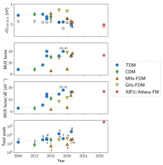
Figure 14.
Progress on the multiplexing read-out of TES X-ray microcalorimeters over the last decade. From top to bottom it is shown, for each multiplexing configuration: the multiplexed energy resolution, , for photons at 5.9 keV energy, the multiplexing factor per channel, the multiplexing factor per channel normalized to the energy resolution, and the total number of pixels read-out simultaneously in multi-channel experiments. The empty symbols on the top plot correspond to the energy resolution measured in single pixel mode in the corresponding multiplexing experiments. The star symbol is the expected demonstration of the readout of 3168 pixels with the XIFU/Athena flight model (FM). The data points are taken from the following publications, as annotated in the bottom plot: a = [195], b = [196], c = [9], d = [133], e = [197], f = [128] (32 TESs + 8 repeats of the last row), g = [134], h = [135], i = [10], j = [198], k = [127], l = [148], m = [149], n = [114], o = [157].
Author Contributions
Conceptualization, writing and editing, L.G.; K.N. took care of the conceptualization and writing of the section on the detector fabrication. All authors have read and agreed to the published version of the manuscript.
Funding
This work is partly funded by European Space Agency (ESA) under ESA CTP contract ITT AO/1-7947/14/NL/BW and ESA CTP Contract No. 4000130346/20/NL/BW/os, by the European Union’s Horizon 2020 Program under the AHEAD project (Grant Agreement Number 654215) and is part of the research program Athena (project number 184.034.002), which is partly financed by the Dutch Research Council (NWO).
Institutional Review Board Statement
Not applicable.
Informed Consent Statement
Not applicable.
Data Availability Statement
Not applicable.
Acknowledgments
We wish to thank the X-IFU team at SRON for their precious support. In particular, we are grateful to Hiroki Akamatsu, Marcel Bruin, Martin de Wit, Emanuele Taralli, Davide Vaccaro, Matteo d’Andrea, Marcel Ridder, Jan van der Kuur, and Brian Jackson for the helpful discussions and for their valuable contribution to the work presented here. We acknowledge the fruitful collaboration over the past years with Mikko Kiviranta at VTT, Steve Smith, Nick Wakeham, Jay Chervenak, Kazu Sakai at NASA-GSFC, Douglas Bennet at NIST, and Alex Kozorezov at the Lancaster University. We thank Marios Kounalakis from Delft University for reading and commenting the manuscript.
Conflicts of Interest
The authors declare no conflict of interest.
References
- Adams, J.S.; Baker, R.; Bandler, S.R.; Bastidon, N.; Danowski, M.E.; Doriese, W.B.; Eckart, M.E.; Figueroa-Feliciano, E.; Fuhrman, J.; Goldfinger, D.C.; et al. First Operation of Transition-Edge Sensors in Space with the Micro-X Sounding Rocket; Society of Photo-Optical Instrumentation Engineers (SPIE) Conference Series; International Society for Optics and Photonics: Bellingham, WA, USA, 2021; Volume 11454, p. 1145414. [Google Scholar] [CrossRef]
- Barret, D.; Decourchelle, A.; Fabian, A.; Guainazzi, M.; Nandra, K.; Smith, R.; den Herder, J.W. The Athena space X-ray observatory and the astrophysics of hot plasma. Astron. Nachr. 2020, 341, 224–235. [Google Scholar] [CrossRef]
- Sugai, H.; Ade, P.A.R.; Akiba, Y.; Alonso, D.; Arnold, K.; Aumont, J.; Austermann, J.; Baccigalupi, C.; Banday, A.J.; Banerji, R.; et al. Updated Design of the CMB Polarization Experiment Satellite LiteBIRD. J. Low Temp. Phys. 2020, 199, 1107–1117. [Google Scholar] [CrossRef]
- A Ade, P.; Aguirre, J.; Ahmed, Z.; Aiola, S.; Ali, A.; Alonso, D.; Alvarez, M.A.; Arnold, K.; Ashton, P.; Austermann, J.; et al. The Simons Observatory: Science goals and forecasts. J. Cosmol. Astropart. Phys. 2019, 2019, 56. [Google Scholar] [CrossRef]
- Thornton, R.J. The Atacama Cosmology Telescope: The Polarization-sensitive ACTPol Instrument. Astrophys. J. Suppl. Ser. 2016, 227, 21. [Google Scholar] [CrossRef]
- Piat, M.; Stankowiak, G.; Battistelli, E.S.; de Bernardis, P.; Alessandro, G.D.; De Petris, M.; Grandsire, L.; Hamilton, J.C.; Hoang, T.D.; Marnieros, S.; et al. QUBIC IV: Performance of TES Bolometers and Readout Electronics. arXiv 2021, arXiv:2101.06787. [Google Scholar]
- Roelfsema, P.; Giard, M.; Najarro, F.; Wafelbakker, K.; Jellema, W.; Jackson, B.; Sibthorpe, B.; Audard, M.; Doi, Y.; di Giorgio, A.; et al. SAFARI new and improved: Extending the capabilities of SPICA’s imaging spectrometer. In Space Telescopes and Instrumentation 2014: Optical, Infrared, and Millimeter Wave; Clampin, M., Fazio, G.G., MacEwen, H.A., Eds.; International Society for Optics and Photonics, SPIE: Bellingham, WA, USA, 2014; Volume 9143, pp. 419–429. [Google Scholar] [CrossRef]
- Nucciotti, A.; Alpert, B.; Balata, M.; Becker, D.; Bennett, D.; Bevilacqua, A.; Biasotti, M.; Ceriale, V.; Ceruti, G.; Corsini, D.; et al. Status of the HOLMES Experiment to Directly Measure the Neutrino Mass. J. Low Temp. Phys. 2018, 183, 1137–1145. [Google Scholar] [CrossRef]
- Doriese, W.B.; Morgan, K.M.; Bennett, D.A.; Denison, E.V.; Fitzgerald, C.P.; Fowler, J.W.; Gard, J.D.; Hays-Wehle, J.P.; Hilton, G.C.; Irwin, K.D.; et al. Developments in Time-Division Multiplexing of X-ray Transition-Edge Sensors. J. Low Temp. Phys. 2016, 184, 389–395. [Google Scholar] [CrossRef] [PubMed]
- Morgan, K.M.; Alpert, B.K.; Bennett, D.A.; Denison, E.V.; Doriese, W.B.; Fowler, J.W.; Gard, J.D.; Hilton, G.C.; Irwin, K.D.; Joe, Y.I.; et al. Code-division-multiplexed readout of large arrays of TES microcalorimeters. Appl. Phys. Lett. 2016, 109, 112604. [Google Scholar] [CrossRef]
- Mates, J.A.B.; Becker, D.T.; Bennett, D.A.; Dober, B.J.; Gard, J.D.; Hays-Wehle, J.P.; Fowler, J.W.; Hilton, G.C.; Reintsema, C.D.; Schmidt, D.R.; et al. Simultaneous readout of 128 X-ray and gamma-ray transition-edge microcalorimeters using microwave SQUID multiplexing. Appl. Phys. Lett. 2017, 111, 062601. [Google Scholar] [CrossRef]
- van der Kuur, J.; Gottardi, L.; Akamatsu, H.; van Leeuwen, B.J.; den Hartog, R.; Haas, D.; Kiviranta, M.; Jackson, B.J. Optimising the multiplex factor of the frequency domain multiplexed readout of the TES-based microcalorimeter imaging array for the X-IFU instrument on the Athena X-ray observatory. In Space Telescopes and Instrumentation 2016: Ultraviolet to Gamma Ray; den Herder, J.W.A., Takahashi, T., Bautz, M., Eds.; International Society for Optics and Photonics, SPIE: Bellingham, WA, USA, 2016; Volume 9905, pp. 1666–1674. [Google Scholar] [CrossRef]
- McCammon, D. Thermal Equilibrium Calorimeters—An Introduction. In Cryogenic Particle Detection; Enss, C., Ed.; Springer: Berlin/Heidelberg, Germany, 2005; pp. 1–34. [Google Scholar] [CrossRef]
- Irwin, K.; Hilton, G. Transition-Edge Sensors. In Cryogenic Particle Detection; Enss, C., Ed.; Springer: Berlin/Heidelberg, Germany, 2005; pp. 63–150. [Google Scholar] [CrossRef]
- Ullom, J.N.; Bennett, D.A. Review of superconducting transition-edge sensors for X-ray and gamma-ray spectroscopy. Supercond. Sci. Technol. 2015, 28, 084003. [Google Scholar] [CrossRef]
- Barret, D.; Trong, T.L.; Den Herder, J.W.; Piro, L.; Barcons, X.; Huovelin, J.; Kelley, R.; Mas-Hesse, J.M.; Mitsuda, K.; Paltani, S.; et al. The ATHENA X-ray Integral Field Unit (X-IFU). In Space Telescopes and Instrumentation 2018: Ultraviolet to Gamma Ray; den Herder, J.W.A., Nikzad, S., Nakazawa, K., Eds.; International Society for Optics and Photonics, SPIE: Bellingham, WA, USA, 2018; Volume 10699, pp. 324–338. [Google Scholar] [CrossRef]
- Lindeman, M.A.; Bandler, S.; Brekosky, R.P.; Chervenak, J.A.; Figueroa-Feliciano, E.; Finkbeiner, F.M.; Li, M.J.; Kilbourne, C.A. Impedance measurements and modeling of a transition-edge-sensor calorimeter. Rev. Sci. Instrum. 2004, 75, 1283–1289. [Google Scholar] [CrossRef]
- Irwin, K. Thermodynamics of nonlinear bolometers near equilibrium. Nucl. Instrum. Methods Phys. Res. Sect. A 2006, 559, 718–720. [Google Scholar] [CrossRef]
- Irwin, K.D. An application of electrothermal feedback for high resolution cryogenic particle detection. Appl. Phys. Lett. 1995, 66, 1998–2000. [Google Scholar] [CrossRef]
- Sadleir, J.E.; Smith, S.J.; Bandler, S.R.; Chervenak, J.A.; Clem, J.R. Longitudinal Proximity Effects in Superconducting Transition-Edge Sensors. Phys. Rev. Lett. 2010, 104, 047003. [Google Scholar] [CrossRef]
- Sadleir, J.E.; Smith, S.J.; Robinson, I.K.; Finkbeiner, F.M.; Chervenak, J.A.; Bandler, S.R.; Eckart, M.E.; Kilbourne, C.A. Proximity effects and nonequilibrium superconductivity in transition-edge sensors. Phys. Rev. B 2011, 84, 184502. [Google Scholar] [CrossRef]
- de Wit, M.; Gottardi, L.; Taralli, E.; Nagayoshi, K.; Ridder, M.L.; Akamatsu, H.; Bruijn, M.P.; D’Andrea, M.; van der Kuur, J.; Ravensberg, K.; et al. High aspect ratio transition edge sensors for X-ray spectrometry. J. Appl. Phys. 2020, 128, 224501. [Google Scholar] [CrossRef]
- Ridder, M.L.; Nagayoshi, K.; Bruijn, M.P.; Gottardi, L.; Taralli, E.; Khosropanah, P.; Akamatsu, H.; van der Kuur, J.; Ravensberg, K.; Visser, S.; et al. Study of TES Detector Transition Curve to Optimize the Pixel Design for Frequency-Division Multiplexing Readout. J. Low Temp. Phys. 2020, 199, 962–967. [Google Scholar] [CrossRef]
- Likharev, K.K. Superconducting weak links. Rev. Mod. Phys. 1979, 51, 101–159. [Google Scholar] [CrossRef]
- Golubov, A.A.; Kupriyanov, M.Y.; Il’ichev, E. The current-phase relation in Josephson junctions. Rev. Mod. Phys. 2004, 76, 411–469. [Google Scholar] [CrossRef]
- Kupriyanov, M.Y.; Likharev, K.K.; Lukichev, V.F. Influence of effective electron interaction on the critical current of Josephson weak links. Physica 1981, 108B, 1001–1002. [Google Scholar] [CrossRef]
- Kupriyanov, M.Y.; Lukichev, V.F. Influence of the proximity effect in the electrodes on the stationary properties of S–N–S Josephson structures. Sov. J. Low Temp. Phys. 1982, 8, 526–529. [Google Scholar]
- Kozorezov, A.G.; Golubov, A.A.; Martin, D.D.E.; de Korte, P.A.J.; Lindeman, M.A.; Hijmering, R.A.; Wigmore, J.K. Microscopic Model of a Transition Edge Sensor as a Weak Link. IEEE Trans. Appl. Supercond. 2011, 21, 250–253. [Google Scholar] [CrossRef]
- Harwin, R.C.; Goldie, D.J.; Withington, S. Modelling proximity effects in transition edge sensors to investigate the influence of lateral metal structures. Supercond. Sci. Technol. 2017, 30, 084001. [Google Scholar] [CrossRef]
- Harwin, R.C.; Goldie, D.J.; Withington, S.; Khosropanah, P.; Gottardi, L.; Gao, J.R. Proximity effect model for X-ray transition edge sensors. In High Energy, Optical, and Infrared Detectors for Astronomy VIII; Holland, A.D., Beletic, J., Eds.; International Society for Optics and Photonics, SPIE: Bellingham, WA, USA, 2018; Volume 10709, pp. 350–361. [Google Scholar] [CrossRef]
- Kozorezov, A.; Golubov, A.A.; Martin, D.D.E.; de Korte, P.A.J.; Lindeman, M.A.; Hijmering, R.A.; van der Kuur, J.; Hoevers, H.F.C.; Gottardi, L.; Kupriyanov, M.Y.; et al. Modelling the resistive state in a transition edge sensor. Appl. Phys. Lett. 2011, 99, 063503. [Google Scholar] [CrossRef]
- Coffey, W.T.; Kalmykov, Y.P.; Titov, S.V.; Cleary, L. Smoluchowski equation approach for quantum Brownian motion in a tilted periodic potential. Phys. Rev. E 2008, 78, 031114. [Google Scholar] [CrossRef]
- Ambegaokar, V.; Halperin, B.I. Voltage Due to Thermal Noise in the dc Josephson Effect. Phys. Rev. Lett. 1969, 22, 1364–1366. [Google Scholar] [CrossRef]
- Smith, S.J.; Adams, J.S.; Bailey, C.N.; Bandler, S.R.; Busch, S.E.; Chervenak, J.A.; Eckart, M.E.; Finkbeiner, F.M.; Kilbourne, C.A.; Kelley, R.L.; et al. Implications of weak-link behavior on the performance of Mo/Au bilayer transition-edge sensors. J. Appl. Phys. 2013, 114, 074513–074524. [Google Scholar] [CrossRef]
- Smith, S.J.; Adams, J.S.; Bailey, C.N.; Bandler, S.R.; Chervenak, J.A.; Eckart, M.E.; Finkbeiner, F.M.; Kelley, R.L.; Kilbourne, C.A.; Porter, F.S.; et al. Small Pitch Transition-Edge Sensors with Broadband High Spectral Resolution for Solar Physics. J. Low Temp. Phys. 2012, 167, 168–175. [Google Scholar] [CrossRef]
- Gottardi, L.; Akamatsu, H.; Bruijn, M.; Gao, J.R.; den Hartog, R.; Hijmering, R.; Hoevers, H.; Khosropanah, P.; Kozorezov, A.; van der Kuur, J.; et al. Weak-Link Phenomena in AC-Biased Transition Edge Sensors. J. Low Temp. Phys. 2014, 176, 279–284. [Google Scholar] [CrossRef]
- Bennett, D.A.; Swetz, D.S.; Schmidt, D.R.; Ullom, J.N. Resistance in transition-edge sensors: A comparison of the resistively shunted junction and two-fluid models. Phys. Rev. B 2013, 87, 020508. [Google Scholar] [CrossRef]
- Bennett, D.A.; Schmidt, D.R.; Swetz, D.S.; Ullom, J.N. Phase-slip lines as a resistance mechanism in transition-edge sensors. Appl. Phys. Lett. 2014, 104, 042602. [Google Scholar] [CrossRef]
- Irwin, K.D.; Hilton, G.C.; Wollman, D.A.; Martinis, J.M. Thermal-response time of superconducting transition-edge microcalorimeters. J. Appl. Phys. 1998, 83, 3978–3985. [Google Scholar] [CrossRef]
- Bennett, D.A.; Swetz, D.S.; Horansky, R.D.; Schmidt, D.R.; Ullom, J.N. A Two-Fluid Model for the Transition Shape in Transition-Edge Sensors. J. Low Temp. Phys. 2012, 167, 102–107. [Google Scholar] [CrossRef]
- Morgan, K.M.; Pappas, C.G.; Bennett, D.A.; Gard, J.D.; Hays-Wehle, J.P.; Hilton, G.C.; Reintsema, C.D.; Schmidt, D.R.; Ullom, J.N.; Swetz, D.S. Dependence of transition width on current and critical current in transition-edge sensors. Appl. Phys. Lett. 2017, 110, 212602. [Google Scholar] [CrossRef]
- Morgan, K.M.; Becker, D.T.; Bennett, D.A.; Doriese, W.B.; Gard, J.D.; Irwin, K.D.; Lee, S.J.; Li, D.; Mates, J.A.B.; Pappas, C.G.; et al. Use of Transition Models to Design High Performance TESs for the LCLS-II Soft X-ray Spectrometer. IEEE Trans. Appl. Supercond. 2019, 29, 1–5. [Google Scholar] [CrossRef]
- Kupriyanov, M.Y.; Likharev, K.K.; Lukichev, V.F. The Js(ψ) Relationship, Abrikosov Vortices and Josephson Vortices in Variable Thickness Bridges; North-Holland: Amsterdam, The Netherlands, 1975. [Google Scholar]
- Smith, S. Studies of weak-link phenomena in Mo/Au TESs. In Poster Presentation. TES Workshop. Applied Superc. Conference 2014; ASC Inc.: Charlotte, NC, USA, 2014. [Google Scholar]
- Sadleir, J. Unexpected nonlinear effects in superconducting Transition-Edge Sensors. In TES workshop. Applied Superc. Conference 2016; ASC Inc.: Denver, CO, USA, 2016. [Google Scholar]
- Zhou, Y.; Ambarish, C.V.; Gruenke, R.; Jaeckel, F.T.; Kripps, K.L.; McCammon, D.; Morgan, K.M.; Wulf, D.; Zhang, S.; Adams, J.S.; et al. Mapping TES Temperature Sensitivity and Current Sensitivity as a Function of Temperature, Current, and Magnetic Field with IV Curve and Complex Admittance Measurements. J. Low Temp. Phys. 2018, 193, 321–327. [Google Scholar] [CrossRef]
- Fraser, G. On the nature of the superconducting-to-normal transition in transition edge sensors. Nucl. Instrum. Methods Phys. Res. Sect. A Accel. Spectrom. Detect. Assoc. Equip. 2004, 523, 234–245. [Google Scholar] [CrossRef]
- Fàbrega, L.; Camón, A.; Pobes, C.; Strichovanec, P.; González-Arrabal, R. Large current-induced broadening of the superconducting transition in Mo/Au transition edge sensors. Supercond. Sci. Technol. 2018, 32, 015006. [Google Scholar] [CrossRef]
- Lindeman, M.A.; Dirks, B.; van der Kuur, J.; de Korte, P.A.J.; den Hartog, R.H.; Gottardi, L.; Hijmering, R.A.; Hoevers, H.F.C.; Khosropanah, P. Relationships Between Complex Impedance, Thermal Response, and Noise in TES Calorimeters and Bolometers. IEEE Trans. Appl. Supercond. 2011, 21, 254–257. [Google Scholar] [CrossRef]
- Takei, Y.; Gottardi, L.; Hoevers, H.F.C.; de Korte, P.A.J.; van der Kuur, J.; Ridder, M.L.; Bruijn, M.P. Characterization of a High-Performance Ti/Au TES Microcalorimeter with a Central Cu Absorber. J. Low Temp. Phys. 2008, 151, 161–166. [Google Scholar] [CrossRef]
- Kinnunen, K.M.; Palosaari, M.R.J.; Maasilta, I.J. Normal metal-superconductor decoupling as a source of thermal fluctuation noise in transition-edge sensors. J. Appl. Phys. 2012, 112, 034515. [Google Scholar] [CrossRef]
- Maasilta, I.J. Complex impedance, responsivity and noise of transition-edge sensors: Analytical solutions for two- and three-block thermal models. AIP Adv. 2012, 2, 042110. [Google Scholar] [CrossRef]
- Goldie, D.J.; Audley, M.D.; Glowacka, D.M.; Tsaneva, V.N.; Withington, S. Thermal models and noise in transition edge sensors. J. Appl. Phys. 2009, 105, 074512. [Google Scholar] [CrossRef]
- Wakeham, N.A.; Adams, J.S.; Bandler, S.R.; Beaumont, S.; Chervenak, J.A.; Datesman, A.M.; Eckart, M.E.; Finkbeiner, F.M.; Hummatov, R.; Kelley, R.L.; et al. Thermal fluctuation noise in Mo/Au superconducting transition-edge sensor microcalorimeters. J. Appl. Phys. 2019, 125, 164503. [Google Scholar] [CrossRef]
- Bruijn, M.P.; van der Linden, A.J.; Ferrari, L.; Gottardi, L.; van der Kuur, J.; den Hartog, R.H.; Akamatsu, H.; Jackson, B.D. LC Filters for FDM Readout of the X-IFU TES Calorimeter Instrument on Athena. J. Low Temp. Phys. 2018, 193, 661–667. [Google Scholar] [CrossRef]
- Bruijn, M.P.; Gottardi, L.; den Hartog, R.H.; van der Kuur, J.; van der Linden, A.J.; Jackson, B.D. Tailoring the High-Q LC Filter Arrays for Readout of Kilo-Pixel TES Arrays in the SPICA-SAFARI Instrument. J. Low Temp. Phys. 2014, 176, 421–425. [Google Scholar] [CrossRef]
- Kiviranta, M.; Seppä, H.; van der Kuur, J.; de Korte, P. SQUID-based readout schemes for microcalorimeter arrays. AIP Conf. Proc. 2002, 605, 295–300. [Google Scholar] [CrossRef]
- Gottardi, L.; van der Kuur, J.; Bruijn, M.; van der Linden, A.; Kiviranta, M.; Akamatsu, H.; den Hartog, R.; Ravensberg, K. Intrinsic Losses and Noise of High- Q Lithographic MHz LC Resonators for Frequency Division Multiplexing. J. Low Temp. Phys. 2019, 194, 370–376. [Google Scholar] [CrossRef]
- van der Kuur, J.; Gottardi, L.; Borderias, M.P.; Dirks, B.; de Korte, P.; Lindeman, M.; Khosropanah, P.; den Hartog, R.; Hoevers, H. Small-Signal Behavior of a TES Under AC Bias. IEEE Trans. Appl. Supercond. 2011, 21, 281–284. [Google Scholar] [CrossRef]
- Taralli, E.; Khosropanah, P.; Gottardi, L.; Nagayoshi, K.; Ridder, M.L.; Bruijn, M.P.; Gao, J.R. Complex impedance of TESs under AC bias using FDM readout system. AIP Adv. 2019, 9, 045324. [Google Scholar] [CrossRef]
- Gottardi, L.; Kozorezov, A.; Akamatsu, H.; van der Kuur, J.; Bruijn, M.P.; den Hartog, R.H.; Hijmering, R.; Khosropanah, P.; Lambert, C.; van der Linden, A.J.; et al. Josephson effects in an alternating current biased transition edge sensor. Appl. Phys. Lett. 2014, 105, 162605. [Google Scholar] [CrossRef]
- Coffey, W.T.; Kalmykov, Y.P.; Titov, S.V.; Cleary, L. Nonlinear noninertial response of a quantum Brownian particle in a tilted periodic potential to a strong ac force as applied to a point Josephson junction. Phys. Rev. B 2009, 79, 054507. [Google Scholar] [CrossRef]
- Coffey, W.T.; Déjardin, J.L.; Kalmykov, Y.P. Nonlinear impedance of a microwave-driven Josephson junction with noise. Phys. Rev. B 2000, 62, 3480–3487. [Google Scholar] [CrossRef]
- Gottardi, L.; Akamatsu, H.; van der Kuur, J.; Smith, S.J.; Kozorezov, A.; Chervenak, J. Study of TES-Based Microcalorimeters of Different Size and Geometry Under AC Bias. IEEE Trans. Appl. Supercond. 2017, 27, 1–4. [Google Scholar] [CrossRef]
- McDonald, J.; Clem, J.R. Microwave response and surface impedance of weak links. Phys. Rev. B 1997, 56, 14723–14732. [Google Scholar] [CrossRef]
- Kirsch, C.; Gottardi, L.; Lorenz, M.; Dauser, T.; den Hartog, R.; Jackson, B.; Peille, P.; Smith, S.; Wilms, J. Time-Domain Modeling of TES Microcalorimeters Under AC Bias. J. Low Temp. Phys. 2020, 199, 569–576. [Google Scholar] [CrossRef]
- Wilms, J.; Smith, S.J.; Peille, P.; Ceballos, M.T.; Cobo, B.; Dauser, T.; Brand, T.; den Hartog, R.H.; Bandler, S.R.; de Plaa, J.; et al. TESSIM: A simulator for the Athena-X-IFU. In Space Telescopes and Instrumentation 2016: Ultraviolet to Gamma Ray; den Herder, J.W.A., Takahashi, T., Bautz, M., Eds.; International Society for Optics and Photonics, SPIE: Bellingham, WA, USA, 2016; Volume 9905, pp. 1795–1801. [Google Scholar] [CrossRef]
- Lorenz, M.; Kirsch, C.; Merino-Alonso, P.E.; Peille, P.; Dauser, T.; Cucchetti, E.; Smith, S.J.; Wilms, J. GPU Supported Simulation of Transition-Edge Sensor Arrays. J. Low Temp. Phys. 2020, 200, 277–285. [Google Scholar] [CrossRef]
- Jaeckel, F.T.; Ambarish, C.V.; Christensen, N.; Gruenke, R.; Hu, L.; McCammon, D.; McPheron, M.; Meyer, M.; Nelms, K.L.; Roy, A.; et al. Energy Calibration of High-Resolution X-ray TES Microcalorimeters With 3 eV Optical Photons. IEEE Trans. Appl. Supercond. 2019, 29, 1–4. [Google Scholar] [CrossRef]
- Jaeckel, F.T.; Ambarish, C.V.; Dai, H.; Liu, S.; Mccammon, D.; Mcpheron, M.; Nelms, K.L.; Roy, A.; Stueber, H.R.; Bandler, S.R.; et al. Calibration and Testing of Small High-Resolution Transition Edge Sensor Microcalorimeters with Optical Photons. IEEE Trans. Appl. Supercond. 2021, 31, 1–5. [Google Scholar] [CrossRef]
- Hoevers, H.F.C.; Bento, A.C.; Bruijn, M.P.; Gottardi, L.; Korevaar, M.A.N.; Mels, W.A.; de Korte, P.A.J. Thermal fluctuation noise in a voltage biased superconducting transition edge thermometer. Appl. Phys. Lett. 2000, 77, 4422–4424. [Google Scholar] [CrossRef]
- Gildemeister, J.M.; Lee, A.T.; Richards, P.L. Model for excess noise in voltage-biased superconducting bolometers. Appl. Opt. 2001, 40, 6229–6235. [Google Scholar] [CrossRef]
- Khosropanah, P.; Hijmering, R.A.; Ridder, M.; Lindeman, M.A.; Gottardi, L.; Bruijn, M.; Kuur, J.; Korte, P.A.J.; Gao, J.R.; Hoevers, H. Distributed TES Model for Designing Low Noise Bolometers Approaching SAFARI Instrument Requirements. J. Low Temp. Phys. 2012, 167, 188–194. [Google Scholar] [CrossRef][Green Version]
- Ullom, J.; Doriese, W.; Hilton, G.; Beall, J.; Deiker, S.; Irwin, K.; Reintsema, C.; Vale, L.; Xu, Y. Suppression of excess noise in Transition-Edge Sensors using magnetic field and geometry. Nucl. Instrum. Methods A 2004, 520, 333–335. [Google Scholar] [CrossRef]
- Jethava, N.; Ullom, J.N.; Irwin, K.D.; Doriese, W.B.; Beall, J.A.; Hilton, G.C.; Vale, L.R.; Zink, B. Dependence of Excess Noise on the Partial Derivatives of Resistance in Superconducting Transition Edge Sensors. AIP Conf. Proc. 2009, 1185, 31–33. [Google Scholar] [CrossRef]
- Wakeham, N.A.; Adams, J.S.; Bandler, S.R.; Chervenak, J.A.; Datesman, A.M.; Eckart, M.E.; Finkbeiner, F.M.; Kelley, R.L.; Kilbourne, C.A.; Miniussi, A.R.; et al. Effects of Normal Metal Features on Superconducting Transition-Edge Sensors. J. Low Temp. Phys. 2018, 193, 231–240. [Google Scholar] [CrossRef]
- Kozorezov, A.; Golubov, A.; Martin, D.; de Korte, P.; Lindeman, M.; Hijmering, R.; van der Kuur, J.; Hoevers, H.; Gottardi, L.; Kupriyanov, M.; et al. Electrical Noise in a TES as a Resistively Shunted Conducting Junction. J. Low Temp. Phys. 2012, 167, 108–113. [Google Scholar] [CrossRef]
- Likharev, K.; Semenov, V. Fluctuation Spectrum in Superconducting Point Junctions. Sov. Phys. JEPT Lett. 1972, 15, 442. [Google Scholar]
- Koch, R.H.; Van Harlingen, D.J.; Clarke, J. Quantum-Noise Theory for the Resistively Shunted Josephson Junction. Phys. Rev. Lett. 1980, 45, 2132–2135. [Google Scholar] [CrossRef]
- Wessel, A.; Morgan, K.; Becker, D.; Gard, J.; Hilton, G.; Mates, J.; Reintsema, C.; Schmidt, D.R.; Swetz, D.; Ullom, J.; et al. A Model for Excess Johnson Noise in Superconducting Transition-edge Sensors. arXiv 2019, arXiv:1907.11343. [Google Scholar]
- Kogan, S.M.; Nagaev, K. Fluctuation kinetics in superconductors at frequencies low compared with the energy gap. Zh. Eksp. Teor. Fiz 1988, 94, 262. [Google Scholar]
- Gottardi, L.; de Wit, M.; Kozorezov, A.; Taralli, E.; Nagayashi, K. Voltage fluctuations in ac biased superconducting transition edge sensors. Phys. Rev. Lett. 2021. accepted paper. [Google Scholar]
- Andrews, D.H.; Brucksch, W.F.; Ziegler, W.T.; Blanchard, E.R. Superconducting Films as Radiometric Receivers. Phys. Rev. 1941, 59, 1045–1046. [Google Scholar] [CrossRef]
- Gaskin, J.A.; Swartz, D.A.; Vikhlinin, A.; Özel, F.; Gelmis, K.E.; Arenberg, J.W.; Bandler, S.R.; Bautz, M.W.; Civitani, M.M.; Dominguez, A.; et al. Lynx X-ray Observatory: An overview. J. Astron. Telesc. 2019, 5, 021001. [Google Scholar] [CrossRef]
- Simionescu, A.; Ettori, S.; Werner, N.; Nagai, D.; Vazza, F.; Akamatsu, H.; Pinto, C.; de Plaa, J.; Wijers, N.; Nelson, D.; et al. Voyage through the Hidden Physics of the Cosmic Web. arXiv 2019, arXiv:1908.01778. [Google Scholar]
- Rothe, J.; Angloher, G.; Bauer, P.; Bento, A.; Bucci, C.; Canonica, L.; D’Addabbo, A.; Defay, X.; Erb, A.; Feilitzsch, F.V.; et al. TES-Based Light Detectors for the CRESST Direct Dark Matter Search. J. Low Temp. Phys. 2018, 193, 1160–1166. [Google Scholar] [CrossRef]
- Lita, A.E.; Rosenberg, D.; Nam, S.; Miller, A.J.; Balzar, D.; Kaatz, L.M.; Schwall, R.E. Tuning of tungsten thin film superconducting transition temperature for fabrication of photon number resolving detectors. IEEE Trans. Appl. Supercond. 2005, 15, 3528–3531. [Google Scholar] [CrossRef]
- Hubmayr, J.; Austermann, J.E.; Beall, J.A.; Becker, D.; Bennett, D.A.; Benson, B.A.; Bleem, L.E.; Chang, C.L.; Carlstrom, J.E.; Cho, H.; et al. Stability of Al-Mn Transition Edge Sensors for Frequency Domain Multiplexing. IEEE Trans. Appl. Supercond. 2011, 21, 203–206. [Google Scholar] [CrossRef]
- Nagayoshi, K.; Ridder, M.L.; Bruijn, M.P.; Gottardi, L.; Taralli, E.; Khosropanah, P.; Akamatsu, H.; Visser, S.; Gao, J.R. Development of a Ti/Au TES Microcalorimeter Array as a Backup Sensor for the Athena/X-IFU Instrument. J. Low Temp. Phys. 2020, 199, 943–948. [Google Scholar] [CrossRef]
- Finkbeiner, F.M.; Adams, J.S.; Bandler, S.R.; Betancourt-Martinez, G.L.; Brown, A.D.; Chang, M.P.; Chervenak, J.A.; Chiao, M.P.; Datesman, A.M.; Eckart, M.E.; et al. Electron-Beam Deposition of Superconducting Molybdenum Thin Films for the Development of Mo/Au TES X-ray Microcalorimeter. IEEE Trans. Appl. Supercond. 2017, 27, 2633785. [Google Scholar] [CrossRef]
- Parra-Borderias, M.; Fernandez-Martinez, I.; Fabrega, L.; Camon, A.; Gil, O.; Costa-Kramer, J.L.; Gonzalez-Arrabal, R.; Sese, J.; Bueno, J.; Briones, F. Characterization of a Mo/Au Thermometer for ATHENA. IEEE Trans. Appl. Supercond. 2013, 23, 2300405. [Google Scholar] [CrossRef]
- Fabrega, L.; Fernandez-Martinez, I.; Gil, O.; Parra-Borderias, M.; Camon, A.; Costa-Kramer, J.; Gonzalez-Arrabal, R.; Sese, J.; Briones, F.; Santiso, J.; et al. Mo-Based Proximity Bilayers for TES: Microstructure and Properties. IEEE Trans. Appl. Supercond. 2009, 19, 460–464. [Google Scholar] [CrossRef]
- Chervenak, J.A.; Finkbeiner, F.M.; Bandler, S.R.; Brekosky, R.; Brown, A.D.; Iyomoto, N.; Kelley, R.L.; Kilbourne, C.A.; Porter, F.S.; Sadleir, J.; et al. Materials Development for Auxiliary Components for Large Compact Mo/Au TES Arrays. J. Low Temp. Phys. 2008, 151, 255–260. [Google Scholar] [CrossRef]
- Orlando, A.; Ceriale, V.; Ceruti, G.; De Gerone, M.; Faverzani, M.; Ferri, E.; Gallucci, G.; Giachero, A.; Nucciotti, A.; Puiu, A.; et al. Microfabrication of Transition-Edge Sensor Arrays of Microcalorimeters with 163Ho for Direct Neutrino Mass Measurements with HOLMES. J. Low Temp. Phys. 2018, 193, 771–776. [Google Scholar] [CrossRef]
- Kunieda, Y.; Takahashi, H.; Zen, N.; Damayanthi, R.; Mori, F.; Fujita, K.; Nakazawa, M.; Fukuda, D.; Ohkubo, M. Characterization of Ir/Au pixel TES. Nucl. Instrum. Methods Phys. Res. Sect. A Accel. Spectrom. Detect. Assoc. Equip. 2006, 559, 429–431. [Google Scholar] [CrossRef]
- Lolli, L.; Taralli, E.; Portesi, C.; Rajteri, M.; Monticone, E. Aluminum–Titanium Bilayer for Near-Infrared Transition Edge Sensors. Sensors 2016, 16, 953. [Google Scholar] [CrossRef] [PubMed]
- Ahmad, K.; Liu, J.; Liu, Q.; Li, G.; Liu, J.; Chen, W. Fabrication and Characterization of Superconducting Bilayer (Al/Ti) Transition-Edge Sensor Bolometer Array. J. Electron. Mater. 2019, 48, 925–929. [Google Scholar] [CrossRef]
- Huang, R.; Zhong, X.F.; Zhang, B.; Koza, J.; Smith, S.; Simmons, S. Super planarizing material for trench and via arrays. In Advances in Patterning Materials and Processes XXXVII; Gronheid, R., Sanders, D.P., Eds.; International Society for Optics and Photonics, SPIE: Bellingham, WA, USA, 2020; Volume 11326, pp. 317–323. [Google Scholar] [CrossRef]
- Devasia, A.M.; Balvin, M.A.; Bandler, S.R.; Bolkhovsky, V.; Nagler, P.C.; Ryu, K.; Smith, S.J.; Stevenson, T.R.; Yoon, W. Fabrication of Magnetic Calorimeter Arrays With Buried Wiring. IEEE Trans. Appl. Supercond. 2019, 29, 1–6. [Google Scholar] [CrossRef]
- Yohannes, D.T.; Hunt, R.T.; Vivalda, J.A.; Amparo, D.; Cohen, A.; Vernik, I.V.; Kirichenko, A.F. Planarized, Extendible, Multilayer Fabrication Process for Superconducting Electronics. IEEE Trans. Appl. Supercond. 2015, 25, 2365562. [Google Scholar] [CrossRef]
- Ridder, M.L.; Khosropanah, P.; Hijmering, R.A.; Suzuki, T.; Bruijn, M.P.; Hoevers, H.F.C.; Gao, J.R.; Zuiddam, M.R. Fabrication of Low-Noise TES Arrays for the SAFARI Instrument on SPICA. J. Low Temp. Phys. 2016, 184, 60–65. [Google Scholar] [CrossRef]
- Bandler, S.R.; Chervenak, J.A.; Datesman, A.M.; Devasia, A.M.; DiPirro, M.J.; Sakai, K.; Smith, S.J.; Stevenson, T.R.; Yoon, W.; Bennett, D.A.; et al. Lynx X-ray microcalorimeter. J. Astron. Telesc. Instrum. Syst. 2019, 5, 1–29. [Google Scholar] [CrossRef]
- Miniussi, A.R.; Adams, J.S.; Bandler, S.R.; Beaumont, S.; Chang, M.P.; Chervenak, J.A.; Finkbeiner, F.M.; Ha, J.Y.; Hummatov, R.; Kelley, R.L.; et al. Thermal Crosstalk Measurements and Simulations for an X-ray Microcalorimeter Array. J. Low Temp. Phys. 2020, 199, 663–671. [Google Scholar] [CrossRef]
- Brown, A.D.; Bandler, S.R.; Brekosky, R.; Chervenak, J.A.; Figueroa-Feliciano, E.; Finkbeiner, F.; Iyomoto, N.; Kelley, R.L.; Kilbourne, C.A.; Porter, F.S.; et al. Absorber Materials for Transition-Edge Sensor X-ray Microcalorimeters. J. Low Temp. Phys. 2008, 151, 413–417. [Google Scholar] [CrossRef]
- Yan, D.; Divan, R.; Gades, L.M.; Kenesei, P.; Madden, T.J.; Miceli, A.; Park, J.S.; Patel, U.M.; Quaranta, O.; Sharma, H.; et al. Eliminating the non-Gaussian spectral response of X-ray absorbers for transition-edge sensors. Appl. Phys. Lett. 2017, 111, 192602. [Google Scholar] [CrossRef]
- Hummatov, R.; Adams, J.S.; Bandler, S.R.; Barlis, A.; Beaumont, S.; Chang, M.P.; Chervenak, J.A.; Datesman, A.M.; Eckart, M.E.; Finkbeiner, F.M.; et al. Quantum Efficiency Study and Reflectivity Enhancement of Au/Bi Absorbers. J. Low Temp. Phys. 2020, 199, 393–400. [Google Scholar] [CrossRef]
- Gottardi, L.; Adams, J.; Bailey, C.; Bandler, S.; Bruijn, M.; Chervenak, J.; Eckart, M.; Finkbeiner, F.; den Hartog, R.; Hoevers, H.; et al. Study of the Dependency on Magnetic Field and Bias Voltage of an AC-Biased TES Microcalorimeter. J. Low Temp. Phys. 2012, 167, 214–219. [Google Scholar] [CrossRef]
- Taralli, E.; Pobes, C.; Khosropanah, P.; Fabrega, L.; Camón, A.; Gottardi, L.; Nagayoshi, K.; Ridder, M.L.; Bruijn, M.P.; Gao, J.R. AC/DC Characterization of a Ti/Au TES with Au/Bi Absorber for X-ray Detection. J. Low Temp. Phys. 2020, 199, 102–109. [Google Scholar] [CrossRef]
- Lindeman, M.A.; Bandler, S.; Brekosky, R.P.; Chervenak, J.A.; Figueroa-Feliciano, E.; Finkbeiner, F.M.; Saab, T.; Stahle, C.K. Characterization and reduction of noise in Mo/Au transition edge sensors. Nucl. Instruments Methods Phys. Res. Sect. A Accel. Spectrom. Detect. Assoc. Equip. 2004, 520, 348–350. [Google Scholar] [CrossRef]
- Smith, S.J.; Adams, J.S.; Bandler, S.R.; Busch, S.E.; Chervenak, J.A.; Eckart, M.E.; Finkbeiner, F.M.; Kelley, R.L.; Kilbourne, C.A.; Lee, S.J.; et al. Characterization of Mo/Au Transition-Edge Sensors with Different Geometric Configurations. J. Low Temp. Phys. 2014, 176, 356–362. [Google Scholar] [CrossRef]
- Zhang, S.; Eckart, M.E.; Jaeckel, F.T.; Kripps, K.L.; McCammon, D.; Morgan, K.M.; Zhou, Y. Mapping of the resistance of a superconducting transition edge sensor as a function of temperature, current, and applied magnetic field. J. Appl. Phys. 2017, 121, 074503. [Google Scholar] [CrossRef]
- Swetz, D.; Bennett, D.; Irwin, K.; Schmidt, D.; Ullom, J. Current distribution and transition width in superconducting transition-edge sensors. Appl. Phys. Lett. 2012, 101, 242603. [Google Scholar] [CrossRef]
- Miniussi, A.R.; Adams, J.S.; Bandler, S.R.; Chervenak, J.A.; Datesman, A.M.; Eckart, M.E.; Ewin, A.J.; Finkbeiner, F.M.; Kelley, R.L.; Kilbourne, C.A.; et al. Performance of an X-ray Microcalorimeter with a 240 m Absorber and a 50 m TES Bilayer. J. Low Temp. Phys. 2018, 193, 337–343. [Google Scholar] [CrossRef]
- Yoon, W.; Adams, J.S.; Bandler, S.R.; Betancourt-Martinez, G.L.; Chiao, M.P.; Chang, M.; Chervenak, J.A.; Datesman, A.; Eckart, M.E.; Ewin, A.J.; et al. Design and Performance of Hybrid Arrays of Mo/Au Bilayer Transition-Edge Sensors. IEEE Trans. Appl. Supercond. 2017, 27, 1–5. [Google Scholar] [CrossRef]
- Smith, S.J.; Adams, J.S.; Bandler, S.R.; Beaumont, S.; Chervenak, J.A.; Datesman, A.M.; Finkbeiner, F.M.; Hummatov, R.; Kelly, R.L.; Kilbourne, C.A.; et al. Toward 100,000-Pixel Microcalorimeter Arrays Using Multi-absorber Transition-Edge Sensors. J. Low Temp. Phys. 2020, 199, 330–338. [Google Scholar] [CrossRef]
- Sakai, K.; Adams, J.S.; Bandler, S.R.; Beaumont, S.; Chervenak, J.A.; Datesman, A.M.; Finkbeiner, F.M.; Kelley, R.L.; Kilbourne, C.A.; Miniussi, A.R.; et al. Demonstration of Fine-Pitch High-Resolution X-ray Transition-Edge Sensor Microcalorimeters Optimized for Energies below 1 keV. J. Low Temp. Phys. 2020, 199, 949–954. [Google Scholar] [CrossRef]
- Sakai, K.; Adams, J.S.; Bandler, S.R.; Chervenak, J.A.; Datesman, A.M.; Eckart, M.E.; Finkbeiner, F.M.; Kelley, R.L.; Kilbourne, C.A.; Miniussi, A.R.; et al. Study of Dissipative Losses in AC-Biased Mo/Au Bilayer Transition-Edge Sensors. J. Low Temp. Phys. 2018, 193, 356–364. [Google Scholar] [CrossRef]
- Akamatsu, H.; Gottardi, L.; Adams, J.; Bandler, S.; Bruijn, M.; Chervenak, J.; Eckart, M.; Finkbeiner, F.; den Hartog, R.; Hoevers, H.; et al. Performance of TES X-ray Microcalorimeters with AC Bias Read-Out at MHz Frequencies. J. Low Temp. Phys. 2014, 176, 591–596. [Google Scholar] [CrossRef]
- Gottardi, L.; Smith, S.J.; Kozorezov, A.; Akamatsu, H.; van der Kuur, J.; Bandler, S.R.; Bruijn, M.P.; Chervenak, J.A.; Gao, J.R.; den Hartog, R.H.; et al. Josephson Effects in Frequency-Domain Multiplexed TES Microcalorimeters and Bolometers. J. Low Temp. Phys. 2018, 193, 209–216. [Google Scholar] [CrossRef]
- Taralli, E.; Gottardi, L.; Nagayoshi, K.; Ridder, M.; Visser, S.; Khosropanah, P.; Akamatsu, H.; van der Kuur, J.; Bruijn, M.; Gao, J.R. Characterization of High Aspect-Ratio TiAu TES X-ray Microcalorimeter Array Under AC Bias. J. Low Temp. Phys. 2020, 199, 80–87. [Google Scholar] [CrossRef]
- Taralli, E.; D’Andrea, M.; Gottardi, L.; Nagayoshi, K.; Ridder, M.L.; de Wit, M.; Vaccaro, D.; Akamatsu, H.; Bruijn, M.P.; Gao, J.R. Performance and uniformity of a kilo-pixel array of Ti/Au transition-edge sensor microcalorimeters. Rev. Sci. Instrum. 2021, 92, 023101. [Google Scholar] [CrossRef]
- D’Andrea, M.; Taralli, E.; Akamatsu, H.; Gottardi, L.; Nagayoshi, K.; Ravensberg, K.; Ridder, M.L.; Vaccaro, D.; de Vries, C.P.; de Wit, M.; et al. Single pixel performance of a 32×32 Ti/Au TES array with broadband X-ray spectra. arXiv 2021, arXiv:2102.08103. [Google Scholar]
- Hoevers, H.F.C.; Ridder, M.L.; Germeau, A.; Bruijn, M.P.; de Korte, P.A.J.; Wiegerink, R.J. Radiative ballistic phonon transport in silicon-nitride membranes at low temperatures. Appl. Phys. Lett. 2005, 86, 251903. [Google Scholar] [CrossRef]
- Hays-Wehle, J.P.; Schmidt, D.R.; Ullom, J.N.; Swetz, D.S. Thermal Conductance Engineering for High-Speed TES Microcalorimeters. J. Low Temp. Phys. 2016, 184, 492–497. [Google Scholar] [CrossRef]
- Doriese, W.B.; Bandler, S.R.; Chaudhuri, S.; Dawson, C.S.; Denison, E.V.; Duff, S.M.; Durkin, M.; FitzGerald, C.T.; Fowler, J.W.; Gard, J.D.; et al. Optimization of Time- and Code-Division-Multiplexed Readout for Athena X-IFU. IEEE Trans. Appl. Supercond. 2019, 29, 1–5. [Google Scholar] [CrossRef]
- Vaccaro, D.; Akamatsu, H.; van der Kuur, J.; van der Hulst, P.; Nieuwenhuizen, A.C.T.; van Winden, P.; Gottardi, L.; den Hartog, R.; Bruijn, M.P.; D’Andrea, M.; et al. Frequency Shift Algorithm: Application to a Frequency-Domain Multiplexing Readout of X-ray Transition-Edge Sensor Microcalorimeters. arXiv 2021, arXiv:2102.06092. [Google Scholar]
- Akamatsu, H.; Gottardi, L.; van der Kuur, J.; de Vries, C.P.; Bruijn, M.P.; Chervenak, J.A.; Kiviranta, M.; van den Linden, A.J.; Jackson, B.D.; Miniussi, A.; et al. Progress in the Development of Frequency-Domain Multiplexing for the X-ray Integral Field Unit on Board the Athena Mission. J. Low Temp. Phys. 2020, 199, 737–744. [Google Scholar] [CrossRef]
- Durkin, M.; Adams, J.S.; Bandler, S.R.; Chervenak, J.A.; Chaudhuri, S.; Dawson, C.S.; Denison, E.V.; Doriese, W.B.; Duff, S.M.; Finkbeiner, F.M.; et al. Demonstration of Athena X-IFU Compatible 40-Row Time-Division-Multiplexed Readout. IEEE Trans. Appl. Supercond. 2019, 29, 1–5. [Google Scholar] [CrossRef]
- Bennett, D.A.; Mates, J.A.B.; Bandler, S.R.; Becker, D.T.; Fowler, J.W.; Gard, J.D.; Hilton, G.C.; Irwin, K.D.; Morgan, K.M.; Reintsema, C.D.; et al. Microwave SQUID multiplexing for the Lynx X-ray microcalorimeter. J. Astron. Telesc. Instrum. Syst. 2019, 5, 1–10. [Google Scholar] [CrossRef]
- Kempf, S.; Wegner, M.; Fleischmann, A.; Gastaldo, L.; Herrmann, F.; Papst, M.; Richter, D.; Enss, C. Demonstration of a scalable frequency-domain readout of metallic magnetic calorimeters by means of a microwave SQUID multiplexer. AIP Adv. 2017, 7, 015007. [Google Scholar] [CrossRef]
- Irwin, K.D. Shannon Limits for Low-Temperature Detector Readout. AIP Conf. Proc. 2009, 1185, 229–236. [Google Scholar]
- Yu, C.; Ames, A.; Chaudhuri, S.; Dawson, C.; Irwin, K.D.; Kuenstner, S.E.; Li, D.; Titus, C.J. An impedance-modulated code-division microwave SQUID multiplexer. Eng. Res. Express 2020, 2, 015011. [Google Scholar] [CrossRef]
- Doriese, W.B.; Abbamonte, P.; Alpert, B.K.; Bennett, D.A.; Denison, E.V.; Fang, Y.; Fischer, D.A.; Fitzgerald, C.P.; Fowler, J.W.; Gard, J.D.; et al. A practical superconducting-microcalorimeter X-ray spectrometer for beamline and laboratory science. Rev. Sci. Instrum. 2017, 88, 053108. [Google Scholar] [CrossRef]
- Smith, S.J.; Adams, J.S.; Bandler, S.R.; Beaumont, S.; Chervenak, J.A.; Denison, E.V.; Doriese, W.B.; Durkin, M.; Finkbeiner, F.M.; Fowler, J.W.; et al. Performance of a Broad-Band, High-Resolution, Transition-Edge Sensor Spectrometer for X-ray Astrophysics. IEEE Trans. Appl. Supercond. 2021, 31, 1–6. [Google Scholar] [CrossRef]
- Stiehl, G.M.; Doriese, W.B.; Fowler, J.W.; Hilton, G.C.; Irwin, K.D.; Reintsema, C.D.; Schmidt, D.R.; Swetz, D.S.; Ullom, J.N.; Vale, L.R. Code-division multiplexing for X-ray microcalorimeters. Appl. Phys. Lett. 2012, 100, 072601. [Google Scholar] [CrossRef]
- Weber, J.C.; Fowler, J.W.; Durkin, M.; Morgan, K.M.; Mates, J.A.B.; Bennett, D.A.; Doriese, W.B.; Schmidt, D.R.; Hilton, G.C.; Swetz, D.S.; et al. Configurable error correction of code-division multiplexed TES detectors with a cryotron switch. Appl. Phys. Lett. 2019, 114, 232602. [Google Scholar] [CrossRef]
- van der Kuur, J.; de Korte, P.; Hoevers, H.; Kiviranta, M.; Seppä, H. Performance of an X-ray microcalorimeter under AC biasing. Appl. Phys. Lett. 2002, 81, 4467–4469. [Google Scholar] [CrossRef]
- Hattori, K.; Akiba, Y.; Arnold, K.; Barron, D.; Bender, A.N.; Cukierman, A.; de Haan, T.; Dobbs, M.; Elleflot, T.; Hasegawa, M.; et al. Development of Readout Electronics for POLARBEAR-2 Cosmic Microwave Background Experiment. J. Low Temp. Phys. 2016, 184, 512–518. [Google Scholar] [CrossRef]
- Bender, A.N.; Anderson, A.J.; Avva, J.S.; Ade, P.A.R.; Ahmed, Z.; Barry, P.S.; Thakur, R.B.; Benson, B.A.; Bryant, L.; Byrum, K.; et al. On-Sky Performance of the SPT-3G Frequency-Domain Multiplexed Readout. J. Low Temp. Phys. 2020, 199, 182–191. [Google Scholar] [CrossRef]
- Bruijn, M.P.; Gottardi, L.; den Hartog, R.H.; Hoevers, H.F.C.; Kiviranta, M.; de Korte, P.A.J.; van der Kuur, J. High-Q LC Filters for FDM Read out of Cryogenic Sensor Arrays. J. Low Temp. Phys. 2012, 167, 695–700. [Google Scholar] [CrossRef]
- Rotermund, K.; Barch, B.; Chapman, S.; Hattori, K.; Lee, A.; Palaio, N.; Shirley, I.; Suzuki, A.; Tran, C. Planar Lithographed Superconducting LC Resonators for Frequency-Domain Multiplexed Readout Systems. J. Low Temp. Phys. 2016, 184, 486–491. [Google Scholar] [CrossRef]
- den Hartog, R.; Audley, M.D.; Beyer, J.; Boersma, D.; Bruijn, M.; Gottardi, L.; Hoevers, H.; Hou, R.; Keizer, G.; Khosropanah, P.; et al. Low-Noise Readout of TES Detectors with Baseband Feedback Frequency Domain Multiplexing. J. Low Temp. Phys. 2012, 167, 652–657. [Google Scholar] [CrossRef][Green Version]
- den Hartog, R.; Boersma, D.; Bruijn, M.; Dirks, B.; Gottardi, L.; Hoevers, H.; Hou, R.; Kiviranta, M.; de Korte, P.; van der Kuur, J.; et al. Baseband Feedback for Frequency-Domain-Multiplexed Readout of TES X-ray Detectors. AIP Conf. Proc. 2009, 1185, 261–264. [Google Scholar] [CrossRef]
- de Haan, T.; Smecher, G.; Dobbs, M. Improved performance of TES bolometers using digital feedback. In Millimeter, Submillimeter, and Far-Infrared Detectors and Instrumentation for Astronomy VI; Holland, W.S., Ed.; International Society for Optics and Photonics, SPIE: Bellingham, WA, USA, 2012; Volume 8452, pp. 113–122. [Google Scholar] [CrossRef]
- van der Kuur, J.; Gottardi, L.; Akamatsu, H.; van Leeuwen, B.J.; den Hartog, R.; Kiviranta, M.; Jackson, B. Thermal Load Minimization of the Frequency Domain Multiplexed Readout for the Athenar X-IFU Instrument. IEEE Trans. Appl. Supercond. 2017, 27, 1–4. [Google Scholar] [CrossRef]
- Kiviranta, M.; Grönberg, L.; Sipola, H. Two-stage locally linearized SQUID readout for frequency domain multiplexed calorimeter arrays. Supercond. Sci. Technol. 2011, 24, 045003. [Google Scholar] [CrossRef][Green Version]
- van der Kuur, J.; Gottardi, L.; Akamatsu, H.; Nieuwenhuizen, A.C.T.; den Hartog, R.; Jackson, B.D. Active Tuning of the Resonance Frequencies of LC Bandpass Filters for Frequency Domain Multiplexed Readout of TES Detector Arrays. J. Low Temp. Phys. 2018, 193, 626–632. [Google Scholar] [CrossRef]
- Akamatsu, H.; Vaccaro, D.; Gottardi, L.; van der Kuur, J.; de Vries, C.P.; Bandler, S.R.; Bruijn, M.P.; Chervenak, J.A.; D’Andrea, M.; Gao, J.R.; et al. Frequency domain multiplexing technology of transition-edge sensors for X-ray astronomy. In Space Telescopes and Instrumentation 2020: Ultraviolet to Gamma Ray; den Herder, J.W.A., Nikzad, S., Nakazawa, K., Eds.; International Society for Optics and Photonics, SPIE: Bellingham, WA, USA, 2020; Volume 11444. [Google Scholar] [CrossRef]
- Akamatsu, H.; Vaccaro, D.; Gottardi, L.; van der Kuur, J.; de Vries, C.P.; Ravensberg, K.; Kiviranta, M.; D’Andrea, M.; Taralli, E.; de Wit, M.; et al. Demonstration of a simultaneous readout of 37 Transition Edge Sensors X-ray microcalorimeters with frequency domain multiplexing. 2021; unpublished work. [Google Scholar]
- Kiviranta, M. Class-B cable-driving SQUID amplifier. arXiv 2020, arXiv:2011.11741. [Google Scholar]
- Kiviranta, M.; Grönberg, L.; van der Kuur, J. Two SQUID amplifiers intended to alleviate the summing node inductance problem in multiplexed arrays of Transition Edge Sensors. arXiv 2018, arXiv:1810.09122. [Google Scholar]
- Irwin, K.D.; Lehnert, K.W. Microwave SQUID multiplexer. Appl. Phys. Lett. 2004, 85, 2107–2109. [Google Scholar] [CrossRef]
- Mates, J.A.B.; Hilton, G.C.; Irwin, K.D.; Vale, L.R.; Lehnert, K.W. Demonstration of a multiplexer of dissipationless superconducting quantum interference devices. Appl. Phys. Lett. 2008, 92, 023514. [Google Scholar] [CrossRef]
- Mates, J.A.B.; Becker, D.T.; Bennett, D.A.; Dober, B.J.; Gard, J.D.; Hilton, G.C.; Swetz, D.S.; Vale, L.R.; Ullom, J.N. Crosstalk in microwave SQUID multiplexers. Appl. Phys. Lett. 2019, 115, 202601. [Google Scholar] [CrossRef]
- Richter, D.; Hoibl, L.; Wolber, T.; Karcher, N.; Fleischmann, A.; Enss, C.; Weber, M.; Sander, O.; Kempf, S. Flux ramp modulation based MHz frequency-division dc-SQUID multiplexer. arXiv 2021, arXiv:2101.06424. [Google Scholar]
- Alpert, B.; Becker, D.; Bennet, D.; Biasotti, M.; Borghesi, M.; Gallucci, G.; De Gerone, M.; Faverzani, M.; Ferri, E.; Fowler, J.; et al. High-resolution high-speed microwave-multiplexed low temperature microcalorimeters for the HOLMES experiment. Eur. Phys. J. C 2019, 79, 304. [Google Scholar] [CrossRef]
- Nakashima, Y.; Hirayama, F.; Kohjiro, S.; Yamamori, H.; Nagasawa, S.; Sato, A.; Yamada, S.; Hayakawa, R.; Yamasaki, N.Y.; Mitsuda, K.; et al. Low-noise microwave SQUID multiplexed readout of 38 X-ray transition-edge sensor microcalorimeters. Appl. Phys. Lett. 2020, 117, 122601. [Google Scholar] [CrossRef]
- Irwin, K.D.; Chaudhuri, S.; Cho, H.M.; Dawson, C.; Kuenstner, S.; Li, D.; Titus, C.J.; Young, B.A. A Spread-Spectrum SQUID Multiplexer. J. Low Temp. Phys. 2018, 193, 476–484. [Google Scholar] [CrossRef]
- Smith, S.J.; Adams, J.S.; Bandler, S.R.; Chervenak, J.A.; Datesman, A.M.; Eckart, M.E.; Finkbeiner, F.M.; Hummatov, R.; Kelley, R.L.; Kilbourne, C.A.; et al. Multiabsorber transition-edge sensors for X-ray astronomy. J. Astron. Telesc. Instrum. Syst. 2019, 5, 1–11. [Google Scholar] [CrossRef]
- Jackson, B.D.; van Weers, H.; van der Kuur, J.; den Hartog, R.; Akamatsu, H.; Argan, A.; Bandler, S.R.; Barbera, M.; Barret, D.; Bruijn, M.P.; et al. The focal plane assembly for the Athena X-ray Integral Field Unit instrument. In Space Telescopes and Instrumentation 2016: Ultraviolet to Gamma Ray; Society of Photo-Optical Instrumentation Engineers (SPIE) Conference Series; den Herder, J.W.A., Takahashi, T., Bautz, M., Eds.; SPIE: Bellingham, WA, USA, 2016; Volume 9905, p. 99052I. [Google Scholar] [CrossRef]
- Geoffray, H.; Jackson, B.; Bandler, S.; Doriese, W.B.; Kirivanta, M.; Prêle, D.; Ravera, L.; Argan, A.; Barbera, M.; van der Kuur, J.; et al. Conceptual design of the detection chain for the X-IFU on Athena. In Space Telescopes and Instrumentation 2020: Ultraviolet to Gamma Ray; den Herder, J.W.A., Nikzad, S., Nakazawa, K., Eds.; International Society for Optics and Photonics, SPIE: Bellingham, WA, USA, 2020; Volume 11444. [Google Scholar] [CrossRef]
- van Weers, H. The X-IFU focal plane assembly development model integration and first test results. In Space Telescopes and Instrumentation 2020: Ultraviolet to Gamma Ray; den Herder, J.W.A., Nikzad, S., Nakazawa, K., Eds.; International Society for Optics and Photonics, SPIE: Bellingham, WA, USA, 2020; Volume 11444. [Google Scholar] [CrossRef]
- Barbera, M.; Cicero, U.L.; Sciortino, L.; D’Anca, F.; Cicero, G.L.; Parodi, G.; Sciortino, S.; Rauw, G.; Branduardi-Raymont, G.; Varisco, S.; et al. ATHENA X-IFU thermal filters development status toward the end of the instrument phase-A. In Space Telescopes and Instrumentation 2018: Ultraviolet to Gamma Ray; den Herder, J.W.A., Nikzad, S., Nakazawa, K., Eds.; International Society for Optics and Photonics, SPIE: Bellingham, WA, USA, 2018; Volume 10699, pp. 406–420. [Google Scholar] [CrossRef]
- Peille, P.; den Hartog, R.; Miniussi, A.; Stever, S.; Bandler, S.; Kirsch, C.; Lorenz, M.; Dauser, T.; Wilms, J.; Lotti, S.; et al. Quantifying the Effect of Cosmic Ray Showers on the X-IFU Energy Resolution. J. Low Temp. Phys. 2020, 199, 240–249. [Google Scholar] [CrossRef]
- Lotti, S.; Macculi, C.; D’Andrea, M.; Fioretti, V.; Dondero, P.; Mantero, A.; Minervini, G.; Argan, A.; Piro, L. Estimates for the background of the ATHENA X-IFU instrument: The cosmic rays contribution. In Space Telescopes and Instrumentation 2018: Ultraviolet to Gamma Ray; den Herder, J.W.A., Nikzad, S., Nakazawa, K., Eds.; International Society for Optics and Photonics, SPIE: Bellingham, WA, USA, 2018; Volume 10699, pp. 397–405. [Google Scholar] [CrossRef]
- Gottardi, L.; van Weers, H.; Dercksen, J.; Akamatsu, H.; Bruijn, M.P.; Gao, J.R.; Jackson, B.; Khosropanah, P.; van der Kuur, J.; Ravensberg, K.; et al. A six-degree-of-freedom micro-vibration acoustic isolator for low-temperature radiation detectors based on superconducting transition-edge sensors. Rev. Sci. Instrum. 2019, 90, 055107. [Google Scholar] [CrossRef]
- Miniussi, A.R.; Adams, J.S.; Bandler, S.R.; Beaumont, S.; Chang, M.P.; Chervenak, J.A.; Finkbeiner, F.M.; Ha, J.Y.; Hummatov, R.; Kelley, R.L.; et al. Thermal Impact of Cosmic Ray Interaction with an X-ray Microcalorimeter Array. J. Low Temp. Phys. 2020, 199, 45–55. [Google Scholar] [CrossRef]
- Lotti, S.; D’Andrea, M.; Molendi, S.; Macculi, C.; Minervini, G.; Fioretti, V.; Laurenza, M.; Jacquey, C.; Piro, L. Review of the Particle Background of the Athena X-IFU Instrument. Astrophys. J. 2021, 909, 111. [Google Scholar] [CrossRef]
- Macculi, C.; Argan, A.; Brienza, D.; D’Andrea, M.; Lotti, S.; Minervini, G.; Piro, L.; Biasotti, M.; Barusso, L.F.; Gatti, F.; et al. The cryogenic anticoincidence detector for ATHENA X-IFU: Advancement in the project. In Space Telescopes and Instrumentation 2020: Ultraviolet to Gamma Ray; den Herder, J.W.A., Nikzad, S., Nakazawa, K., Eds.; International Society for Optics and Photonics, SPIE: Bellingham, WA, USA, 2020; Volume 11444, pp. 686–697. [Google Scholar] [CrossRef]
- Cui, W.; Bregman, J.N.; Bruijn, M.P.; Chen, L.B.; Chen, Y.; Cui, C.; Fang, T.T.; Gao, B.; Gao, H.; Gao, J.R.; et al. HUBS: A Dedicated Hot Circumgalactic Medium Explorer. In Space Telescopes and Instrumentation 2020: Ultraviolet to Gamma Ray; Society of Photo-Optical Instrumentation Engineers (SPIE) Conference Series; SPIE: Bellingham, WA, USA, 2020; Volume 11444, p. 114442S. [Google Scholar]
- Wang, G.; Bruijn, M.; Nagayoshi, K.; Ridder, M.; Taralli, E.; Gottardi, L.; Akamatsu, H.; den Herder, J.W.; Gao, J.R.; Cui, W. Developing X-ray Microcalorimeters Based on TiAu TES for HUBS. In Space Telescopes and Instrumentation 2020: Ultraviolet to Gamma Ray; Society of Photo-Optical Instrumentation Engineers (SPIE) Conference Series; SPIE: Bellingham, WA, USA, 2020; Volume 11444, p. 114449J. [Google Scholar] [CrossRef]
- Sato, K.; Ohashi, T.; Ishisaki, Y.; Ezoe, Y.; Yamada, S.; Yamasaki, N.Y.; Mitsuda, K.; Ishida, M.; Maeda, Y.; Nakashima, Y.; et al. Super DIOS mission for exploring "dark baryon". In Space Telescopes and Instrumentation 2020: Ultraviolet to Gamma Ray; den Herder, J.W.A., Nikzad, S., Nakazawa, K., Eds.; International Society for Optics and Photonics, SPIE: Bellingham, WA, USA, 2020; Volume 11444, pp. 960–969. [Google Scholar] [CrossRef]
- Nakashima, Y.; Hirayama, F.; Kohjiro, S.; Yamamori, H.; Nagasawa, S.; Sato, A.; Yamada, S.; Hayakawa, R.; Yamasaki, N.N.; Mitsuda, K.; et al. Development of microwave multiplexer for the Super DIOS mission: 38 transition-edge sensor X-ray microcalorimeter readout with microwave multiplexing. In X-ray, Optical, and Infrared Detectors for Astronomy IX; Holland, A.D., Beletic, J., Eds.; International Society for Optics and Photonics, SPIE: Bellingham, WA, USA, 2020; Volume 11454, pp. 186–194. [Google Scholar] [CrossRef]
- Particle Data Group; Zyla, P.A.; Barnett, R.M.; Beringer, J.; Dahl, O.; Dwyer, D.A.; Groom, D.E.; Lin, C.-J.; Lugovsky, K.S.; Pianori, E.; et al. Review of Particle Physics. Prog. Theor. Exp. Phys. 2020, 2020, 083C01. [Google Scholar] [CrossRef]
- Aker, M.; Altenmüller, K.; Arenz, M.; Babutzka, M.; Barrett, J.; Bauer, S.; Beck, M.; Beglarian, A.; Behrens, J.; Bergmann, T.; et al. Improved Upper Limit on the Neutrino Mass from a Direct Kinematic Method by KATRIN. Phys. Rev. Lett. 2019, 123, 221802. [Google Scholar] [CrossRef]
- Camilleri, L.; Nucciotti, A. The Use of Low Temperature Detectors for Direct Measurements of the Mass of the Electron Neutrino. Adv. High Energy Phys. 2016, 2016, 9153024. [Google Scholar] [CrossRef]
- Gastaldo, L.; Blaum, K.; Chrysalidis, K.; Goodacre, T.D.; Domula, A.; Door, M.; Dorrer, H.; Düllmann, C.E.; Eberhardt, K.; Eliseev, S.; et al. The electron capture in 163Ho experiment –ECHo. Eur. Phys. J. Spec. Top. 2017, 226, 1623–1694. [Google Scholar] [CrossRef]
- Alpert, B.; Ferri, E.; Bennett, D.; Faverzani, M.; Fowler, J.; Giachero, A.; Hays-Wehle, J.; Maino, M.; Nucciotti, A.; Puiu, A.; et al. Algorithms for Identification of Nearly-Coincident Events in Calorimetric Sensors. J. Low Temp. Phys. 2016, 184, 263–273. [Google Scholar] [CrossRef]
- Ferri, E.; Alpert, B.; Bennett, D.; Faverzani, M.; Fowler, J.; Giachero, A.; Hays-Wehle, J.; Maino, M.; Nucciotti, A.; Puiu, A.; et al. Pile-Up Discrimination Algorithms for the HOLMES Experiment. J. Low Temp. Phys. 2016, 184, 405–411. [Google Scholar] [CrossRef]
- Giachero, A.; Alpert, B.; Becker, D.T.; Bennett, D.A.; Borghesi, M.; De Gerone, M.; Faverzani, M.; Fedkevych, M.; Ferri, E.; Gallucci, G.; et al. Progress in the Development of TES Microcalorimeter Detectors Suitable for Neutrino Mass Measurement. IEEE Trans. Appl. Supercond. 2021, 31, 3051104. [Google Scholar] [CrossRef]
- Peccei, R.D.; Quinn, H.R. CP Conservation in the Presence of Pseudoparticles. Phys. Rev. Lett. 1977, 38, 1440–1443. [Google Scholar] [CrossRef]
- Peccei, R.D.; Quinn, H.R. Constraints imposed by CP conservation in the presence of pseudoparticles. Phys. Rev. D 1977, 16, 1791–1797. [Google Scholar] [CrossRef]
- Jaeckel, J.; Ringwald, A. The Low-Energy Frontier of Particle Physics. Annu. Rev. Nucl. Part. Sci. 2010, 60, 405–437. [Google Scholar] [CrossRef]
- Jaeckel, J.; Thormaehlen, L.J. Distinguishing axion models with IAXO. J. Cosmol. Astropart. Phys. 2019, 2019, 039. [Google Scholar] [CrossRef]
- CAST Collaboration. New CAST limit on the axion–photon interaction. Nat. Phys. 2017, 13, 584–590. [Google Scholar] [CrossRef]
- Armengaud, E.; Avignone, F.T.; Betz, M.; Brax, P.; Brun, P.; Cantatore, G.; Carmona, J.M.; Carosi, G.P.; Caspers, F.; Caspi, S.; et al. Conceptual design of the International Axion Observatory (IAXO). J. Instrum. 2014, 9, T05002. [Google Scholar] [CrossRef]
- Abeln, A.; Altenmüller, K.; Cuendis, S.A.; Armengaud, E.; Attié, D.; Aune, S.; Basso, S.; Bergé, L.; Biasuzzi, B.; De Sousa, P.T.C.; et al. Conceptual Design of BabyIAXO, the intermediate stage towards the International Axion Observatory. arXiv 2020, arXiv:2010.12076. [Google Scholar]
- Unger, D.; Abeln, A.; Enss, C.; Fleischmann, A.; Hengstler, D.; Kempf, S.; Gastaldo, L. High-resolution for IAXO: MMC-based X-ray Detectors. arXiv 2020, arXiv:2010.15348. [Google Scholar]
- Matteo, R. Hunting Season for Primordial Gravitational Waves. APS Phys. 2020, 13, 164. [Google Scholar] [CrossRef]
- Schillaci, A.; Ade, P.A.R.; Ahmed, Z.; Amiri, M.; Barkats, D.; Thakur, R.B.; Bischoff, C.A.; Bock, J.J.; Boenish, H.; Bullock, E.; et al. Design and Performance of the First BICEP Array Receiver. J. Low Temp. Phys. 2020, 199, 976–984. [Google Scholar] [CrossRef]
- Suzuki, A.; Ade, P.; Akiba, Y.; Aleman, C.; Arnold, K.; Baccigalupi, C.; Barch, B.; Barron, D.; Bender, A.; Boettger, D.; et al. The Polarbear-2 and the Simons Array Experiments. J. Low Temp. Phys. 2016, 184, 805–810. [Google Scholar] [CrossRef]
- Hazumi, M.; Ade, P.A.; Akiba, Y.; Alonso, D.; Arnold, K.; Aumont, J.; Baccigalupi, C.; Barron, D.; Basak, S.; Beckman, S.; et al. LiteBIRD: A Satellite for the Studies of B-Mode Polarization and Inflation from Cosmic Background Radiation Detection. J. Low Temp. Phys. 2019, 194, 443–451. [Google Scholar] [CrossRef]
- Jaehnig, G.C.; Arnold, K.; Austermann, J.; Becker, D.; Duff, S.; Halverson, N.W.; Hazumi, M.; Hilton, G.; Hubmayr, J.; Lee, A.T.; et al. Development of Space-Optimized TES Bolometer Arrays for LiteBIRD. J. Low Temp. Phys. 2020, 199, 646–656. [Google Scholar] [CrossRef]
- de Haan, T.; Suzuki, A.; Boyd, S.T.P.; Cantor, R.H.; Coerver, A.; Dobbs, M.A.; Hennings-Yeomans, R.; Holzapfel, W.L.; Lee, A.T.; Noble, G.I.; et al. Recent Advances in Frequency-Multiplexed TES Readout: Vastly Reduced Parasitics and an Increase in Multiplexing Factor with Sub-Kelvin SQUIDs. J. Low Temp. Phys. 2020, 199, 754–761. [Google Scholar] [CrossRef]
- Kilbourne, C.A.; Doriese, W.B.; Bandler, S.R.; Brekosky, R.P.; Brown, A.D.; Chervenak, J.A.; Eckart, M.E.; Finkbeiner, F.M.; Hilton, G.C.; Irwin, K.D.; et al. Multiplexed readout of uniform arrays of TES X-ray microcalorimeters suitable for Constellation-X. In Space Telescopes and Instrumentation 2008: Ultraviolet to Gamma Ray; Turner, M.J.L., Flanagan, K.A., Eds.; Society of Photo-Optical Instrumentation Engineers (SPIE) Conference Series; SPIE: Bellingham, WA, USA, 2008; Volume 7011, p. 701104. [Google Scholar] [CrossRef]
- Smith, S.J.; Adams, J.S.; Bandler, S.R.; Betancourt-Martinez, G.; Chervenak, J.A.; Eckart, M.E.; Finkbeiner, F.M.; Kelley, R.L.; Kilbourne, C.A.; Lee, S.J.; et al. Uniformity of Kilo-Pixel Arrays of Transition-Edge Sensors for X-ray Astronomy. IEEE Trans. Appl. Supercond. 2015, 25, 2369352. [Google Scholar] [CrossRef]
- Ullom, J.N.; Adams, J.S.; Alpert, B.K.; Bandler, S.R.; Bennett, D.A.; Chaudhuri, S.; Chervenak, J.A.; Denison, E.V.; Dawson, C.; Doriese, W.B.; et al. Time- and code-division SQUID multiplexing options for ATHENA X-IFU (Conference Presentation). In Space Telescopes and Instrumentation 2018: Ultraviolet to Gamma Ray; den Herder, J.W.A., Nikzad, S., Nakazawa, K., Eds.; International Society for Optics and Photonics, SPIE: Bellingham, WA, USA, 2018; Volume 10699. [Google Scholar] [CrossRef]
- Akamatsu, H.; Gottardi, L.; van der Kuur, J.; de Vries, C.P.; Ravensberg, K.; Adams, J.S.; Bandler, S.R.; Bruijn, M.P.; Chervenak, J.A.; Kilbourne, C.A.; et al. Development of frequency domain multiplexing for the X-ray Integral Field unit (X-IFU) on the Athena. In Space Telescopes and Instrumentation 2016: Ultraviolet to Gamma Ray; den Herder, J.W.A., Takahashi, T., Bautz, M., Eds.; International Society for Optics and Photonics, SPIE: Bellingham, WA, USA, 2016; Volume 9905, pp. 1675–1682. [Google Scholar] [CrossRef]


Publisher’s Note: MDPI stays neutral with regard to jurisdictional claims in published maps and institutional affiliations. |
© 2021 by the authors. Licensee MDPI, Basel, Switzerland. This article is an open access article distributed under the terms and conditions of the Creative Commons Attribution (CC BY) license (https://creativecommons.org/licenses/by/4.0/).