Article

Novel Wilkinson Power Divider with an Isolation Resistor on a Defected Ground Structure with Improved Isolation

1
Department of Electrical and Communication Systems Engineering, Soonchunhyang University, Asan 336745, Korea
2
Department of Information and Communication Engineering, Soonchunhyang University, Asan 336745, Korea
*
Author to whom correspondence should be addressed.
Appl. Sci. 2021, 11(9), 4148; https://doi.org/10.3390/app11094148
Submission received: 22 February 2021 / Revised: 26 April 2021 / Accepted: 28 April 2021 / Published: 1 May 2021
(This article belongs to the Section Electrical, Electronics and Communications Engineering)

Abstract

:
A modified Wilkinson Power Divider is proposed in this paper that utilizes defected ground structure (DGS) in parallel with an isolation resistor. The proposed DGS section is incorporated between the output ports, and the isolation resistor is soldered in parallel with the DGS in the ground plane, instead of on the top plane as in a conventional Wilkinson power divider, to achieve improved or preferable isolation. The proposed design is comprised of two pairs of microstrip transmission lines with equal impedances and varied electrical lengths. The parameters of the main circuit and the DGS section are acquired separately. The parameters of the proposed main circuit are derived by applying conjugate matching theory. Dumbbell-shaped DGS is introduced in the ground plane between the output ports, which acts as a parallel resonator, yielding an attenuation pole at the resonant frequency that contributes to improved isolation. By applying the previous well-known circuit theory, the lumped elements of the equivalent circuit of the DGS were achieved. The physical dimensions of the equivalent circuit for the DGS section were obtained by three-dimensional EM simulation. The measured results show improved isolation, return loss and better bandwidth as compared with other similar works. Furthermore, the proposed circuits designed at resonating frequencies of 3 and 2 GHz presented comparatively good return losses, S 11 of about −25.54 and −31.24 dB, respectively, and achieved improved isolations, S 32 between the output ports, in an order of about −40.83 and −36.05 dB, respectively, which is rather exceptional and desirable.

1. Introduction

Wilkinson Power Divider (WPD) is a vital component in communication systems and plays an important role in many significant devices, such as mixers and antenna systems [1]. Since the conventional Wilkinson power divider has a simple design method, well-matched ports and relatively good isolation between output ports, it has been widely used as an equal power divider and in several wireless systems. The conventional WPD is an equal power divider and consists of two quarter-wavelength transmission lines. Each transmission line has an impedance of 2 Z 0 , and the isolation resistor of 2 Z 0 is plugged between these lines to achieve good isolation. In contrast, an unequal Wilkinson power divider is comprised of quarter-wave transmission lines having different impedances [2]. Although several reports have addressed the DGS and Wilkinson power divider, the majority of such works were related to the unequal Wilkinson power divider and hybrid couplers by exploiting the effect of change in effective inductance or capacitance of DGS in the ground of a substrate, to reduce the overall size of the circuit or suppress the harmonic effects [3,4,5,6]. In [7], etched DGS is employed in the ground plane to yield an additional effective inductance that results in an unequal impedance between the output ports. Two dumbbell-shaped DGSs are utilized to suppress the harmonics, thus resulting in the reduction of the overall circuit size and complexity [8]. In [9], DGS is introduced in the ground plane to reduce the size of the power divider as well as to improve the performance of the power divider.
As the DGS can also delay the group velocity, with the help of a single cell DGS or single dumbbell-shaped DGS, it is possible to obtain a single attenuation pole or a frequency response characteristic of a low-pass filter [10]. In [11], DGS is proposed to utilize as a resonator by illustrating its applications in various bandpass filter designs. Two dumbbell-shaped DGSs are used to achieve a two-pole bandpass filter, hence proving the equivalent potential of DGS to design dividers, couplers and filters and enhance the performance of respective microwave components. As the dumbbell-shaped DGS can act as a parallel resonator, it thus produces an attenuation pole at a certain frequency [12]. Therefore, this characteristic of DGS can be used to achieve preferable isolation by utilizing it in parallel with the isolation resistor.
In contrast to conventional WPD, which comprises two λ / 4 transmission lines and an isolation resistor soldered on a top plane between these two quarter-wavelength transmission lines, this paper proposes a modified Wilkinson power divider that introduces dumbbell-shaped DGS in the ground plane and the isolation chip resistor is soldered on the DGS to yield desired or better isolation. Each quarter-wave branch of a conventional Wilkinson power divider is substituted by two sections of transmission line with the characteristic impedance of Z 1 and Z 2 and the length of l 1 and l 2 , respectively. The characteristic impedances of both sections Z 1 and Z 2 are fixed at 60 Ω . To design the proposed DGS-powered WPD circuit, the physical dimensions and equivalent lumped circuit parameters of the DGS section and the proposed WPD were extracted by applying the field analysis method and circuit analysis theory. The physical dimensions of the DGS section were obtained separately by performing EM simulation. These methods were successfully applied to extract the required values and dimensions of the proposed equal power divider. The dumbbell-shaped DGS pattern is realized between the output ports, to obtain comparable or preferably better isolation as compared to conventional WPD. Figure 1 shows the layout of the proposed WPD with its DGS section. The goal of the proposed circuit is to achieve better return loss in order of more than −20 dB and improved isolation, i.e., S 32 30 dB in the operating bandwidth.

2. Design Equations

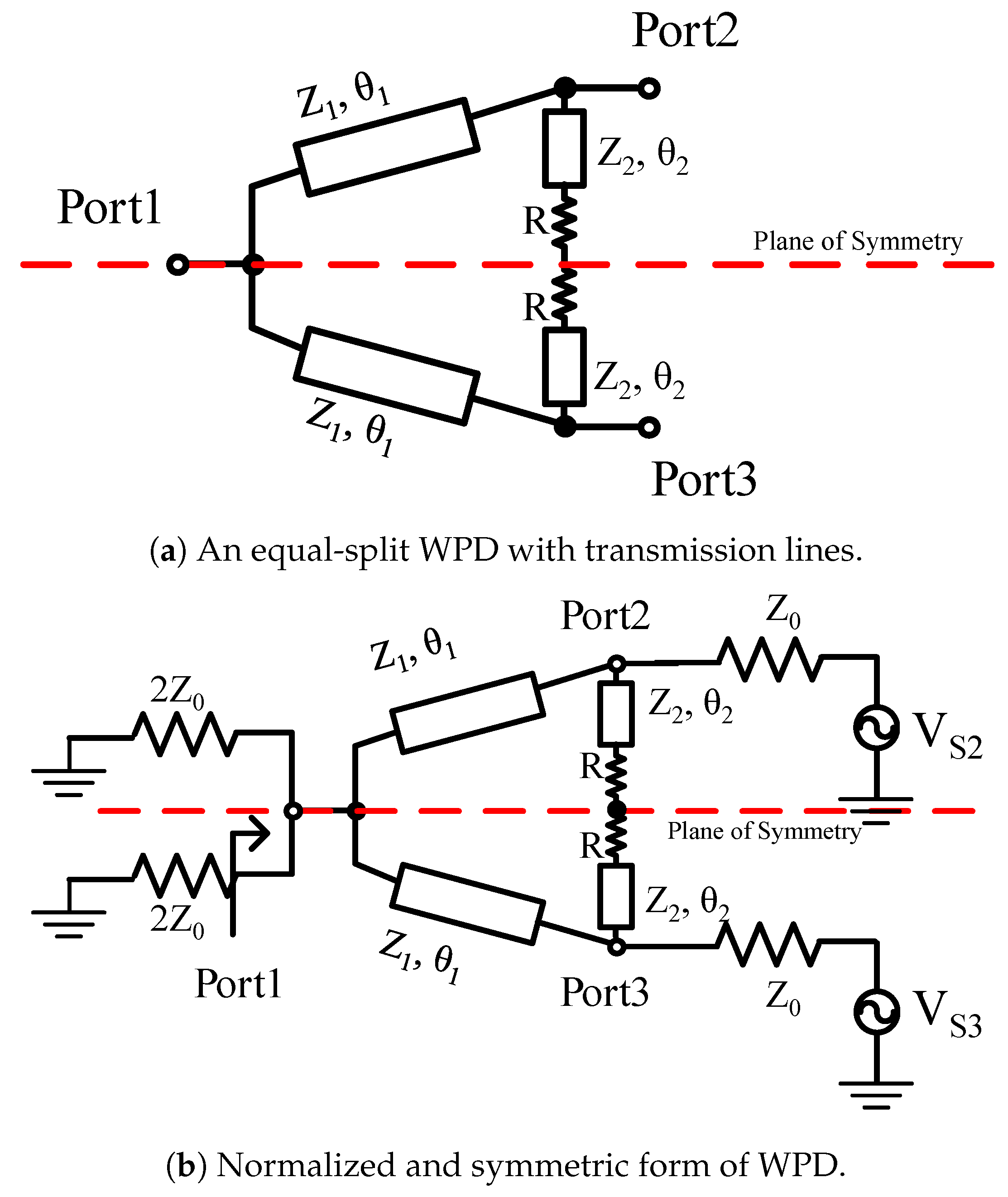
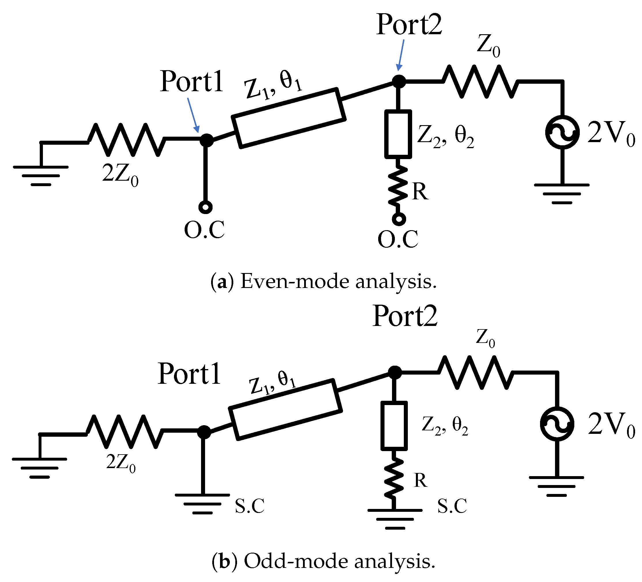
2.1. Even and Odd Mode Analysis without DGS Elements

The conventional WPD is comprised of two transmission lines having an electrical length of quarter wavelength with line impedance of 2 Z 0 and an isolation resistor having a resistance of 2 Z 0 between these transmission lines. Figure 2a shows the proposed circuit, which substitutes these two lines by transmission lines with line impedances Z 1 and Z 2 and electrical lengths θ 1 and θ 2 , respectively. The admittances of the transmission lines with the impedances Z 1 and Z 2 are Y 1 and Y 2 , respectively. where
Y 1 = 1 Z 1 , Y 2 = 1 Z 2 , and Y 0 = 1 Z 0
A lumped resistor 2R is introduced between the transmission lines to achieve maximum isolation. A schematic diagram of the proposed divider, which realizes an equal power division at an arbitrary frequency, is illustrated in Figure 2b. The reference impedance of the circuit is Z 0 . The modeling starts with the even mode analysis by referring to Figure 2b, where the loading impedances Z 0 are considered purely resistive to simplify the circuit evaluation. The circuit given in Figure 2b is symmetric across the midplane, i.e., along the dotted line.Therefore, there is no current flow through the 2R resistor. Thus, the circuit in Figure 2b can be bisected with open circuits at these points to achieve the circuit shown in Figure 3a. Then, the input admittance at Port 2 is obtained as:
Y i n e = Y 1 Y 0 2 + j Y 1 tan θ 1 Y 1 + j Y 0 2 tan θ 1 = Y 1 Y 1 Y 0 2 + Y 1 Y 0 2 tan 2 θ 1 + j tan θ 1 Y 1 2 Y 0 2 2 Y 1 2 + Y 0 2 tan θ 1 2
By applying conjugate matching in Figure 3a, the input admittance at Port 2 is obtained:
Y i n e = Y 0 j Y 2 tan θ 2
By comparing Equations (1) and (2) with respect to their real and complex parts, Equations (3) and (4) are obtained:
1 2 sec 2 θ 1 1 + Y 0 2 Y 1 tan θ 1 2 = 1
Y 1 tan θ 1 Y 1 2 Y 0 2 2 Y 1 2 + Y 0 2 tan θ 1 2 = Y 2 tan θ 2
In the case of odd-mode excitation, because of the symmetry, there is null voltage along the mid-section of the circuit in Figure 2. Considering Port 2, the resistance of the isolation resister is realized as half, i.e., R, as shown in Figure 3b.
The input admittance at Port 2 can be calculated as:
Y i n o = Y 2 1 R + j Y 2 tan θ 2 Y 2 + j 1 R tan θ 2 = Y 2 Y 2 R + Y 2 R tan 2 θ 2 + j tan θ 2 Y 2 2 1 R 2 Y 2 2 + 1 R tan θ 2 2
By applying the conjugate matching in Figure 3b, the input admittance at Port 2 is obtained:
Y i n o = Y 0 + j Y 1 cot θ 1
By comparing Equations (5) and (6) with respect to their real and complex parts, Equations (7) and (8) are obtained:
Y 2 Y 2 R sec 2 θ 2 Y 2 2 + 1 R tan θ 2 2 = Y 0
Y 2 tan θ 2 Y 2 2 1 R 2 Y 2 2 + 1 R tan θ 2 2 = Y 1 cot θ 1
By solving the Equation (3), the electrical length of the admittance line Y 1 is obtained:
tan 2 θ 1 = T 1 = 1 1 2 Y 0 2 Y 1 2 = 1 1 2 β 1
where
β 1 = Y 0 2 Y 1 2
By evaluating Equation (7), the electrical length θ 2 of the transmission line (TL2) is achieved. The electrical length of the admittance line Y 2 is then:
tan 2 θ 2 = T 2 = Y 0 R 1 1 Y 0 R 1 Y 2 R 2 = β 2 R Y 0 R 1 β 2 R 1
where
β 2 = Y 2 2 Y 0
Furthermore, subtracting Equation (4) from Equation (8) yields:
Y 2 tan θ 2 Y 2 2 1 R 2 Y 2 2 + 1 R tan θ 2 2 Y 1 tan θ 1 Y 1 2 Y 0 2 2 Y 1 2 + Y 0 2 tan θ 1 2 = Y 1 cot θ 1 + Y 2 tan θ 2
Equation (13) is rearranged as:
Y 2 tan θ 2 Y 2 2 1 R 2 Y 2 2 + 1 R tan θ 2 2 1 = Y 1 cot θ 1 1 + tan 2 θ 1 Y 1 2 Y 0 2 2 Y 1 2 + Y 0 2 tan θ 1 2
Thus, by inserting T 2 from Equation (11) into Equation (13) and rearranging it, Equation (14) is obtained:
f Y 1 , Y 2 , R = Y 2 T 2 Y 2 2 1 R 2 Y 2 2 + 1 R 2 T 2 1 α = 0
where
α = Y 2 tan θ 2 Y 2 2 1 R 2 Y 2 2 + 1 R tan θ 2 2 1
As Equation (14) is a function of Y 0 , Y 1 , Y 2 and R, Equations (9), (11) and (14) can be plugged into a script or spreadsheet utilizing Matlab or Microsoft Excel, in order to calculate the values of θ 1 , θ 2 and R.

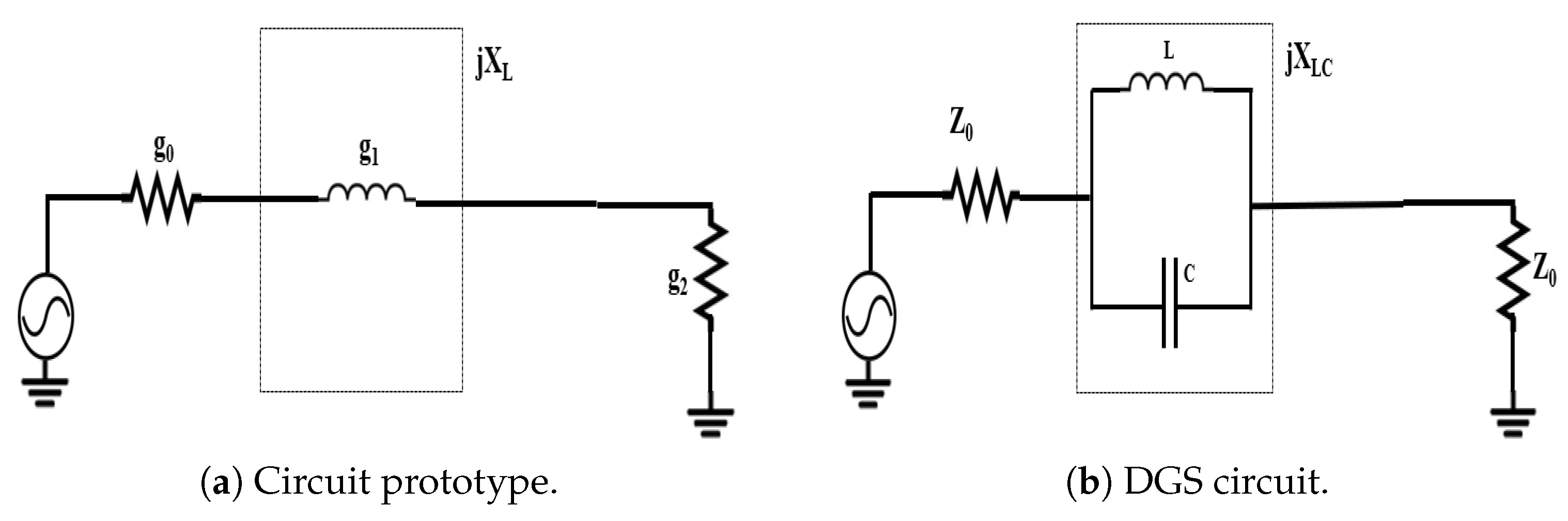
2.2. Parameters Extraction of DGS Section

The parameters of the DGS section were extracted separately. The DGS circuit exhibits the characteristics of a parallel LC circuit. Thus, it can serve as a parallel LC resonator circuit for various purposes in a variety of components. Figure 4a,b shows the equivalent circuits of a one-pole Butterworth-type low-pass filter and its equivalent DGS circuit, respectively [13].
The reactance of the DGS unit is as follows:
X L C = 1 ω 0 C ω 0 ω ω ω 0
where ω 0 is the resonant angular frequency. The series inductance of the Butterworth low-pass filter can be acquired as follows:
X L = ω . Z 0 g 1
where ω is the angular frequency of the 1st-order, one-pole Butterworth prototype low-pass filter and g 1 is the element value, i.e., g 1 = 2.0. To achieve low-pass filter response, the DGS circuit should get an equal net reactance at cutoff frequency ω c as the prototype low-pass filter at ω = 1, i.e.,
X L C | ω = ω c = X L | ω = 1
Thus, from this approximation,
C = ω c Z 0 g 1 1 ω 0 2 ω c 2
and
L = 1 4 π 2 f 0 2 . C
Equations (19) and (20) demonstrate the lumped parameters, i.e., the capacitance and inductance of the DGS circuit. where ω c and f 0 are cutoff angular frequency and resonant frequency, respectively.

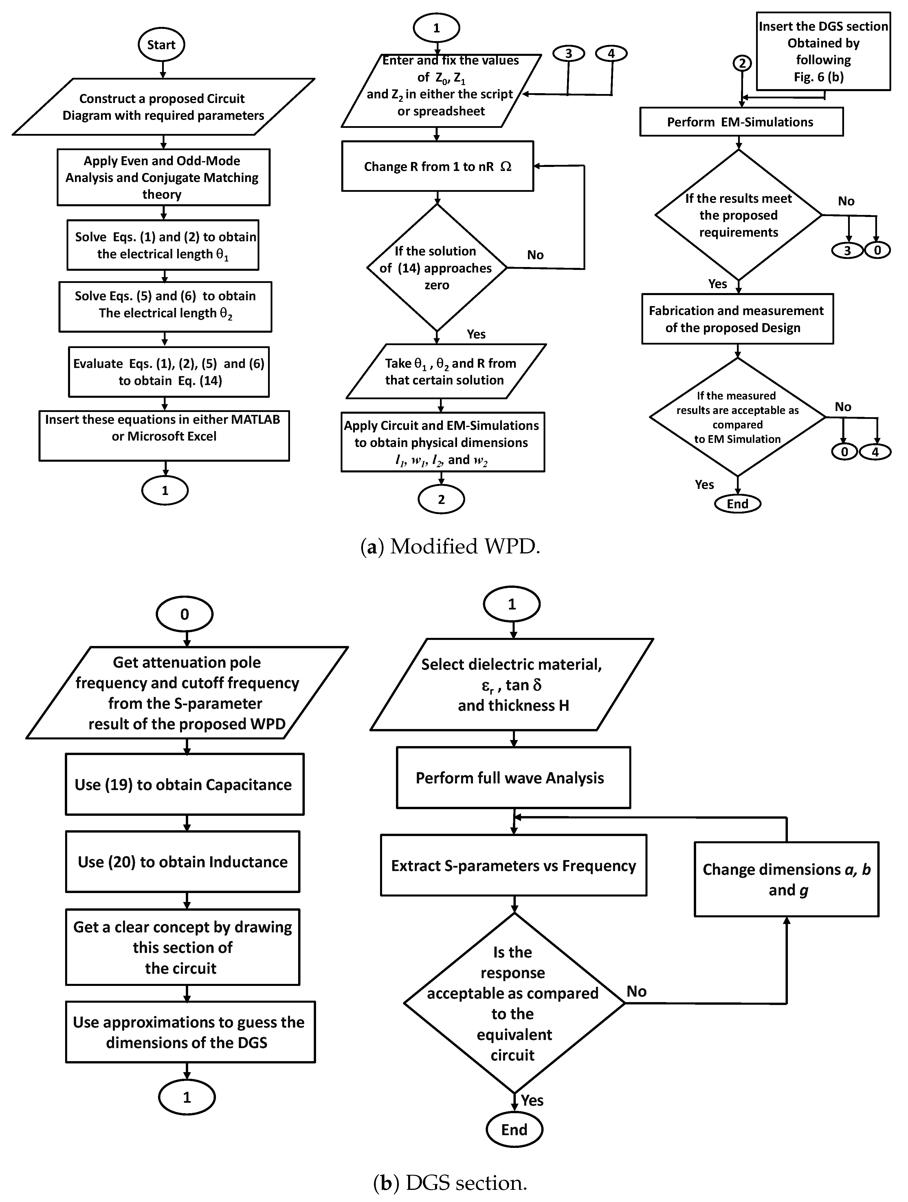
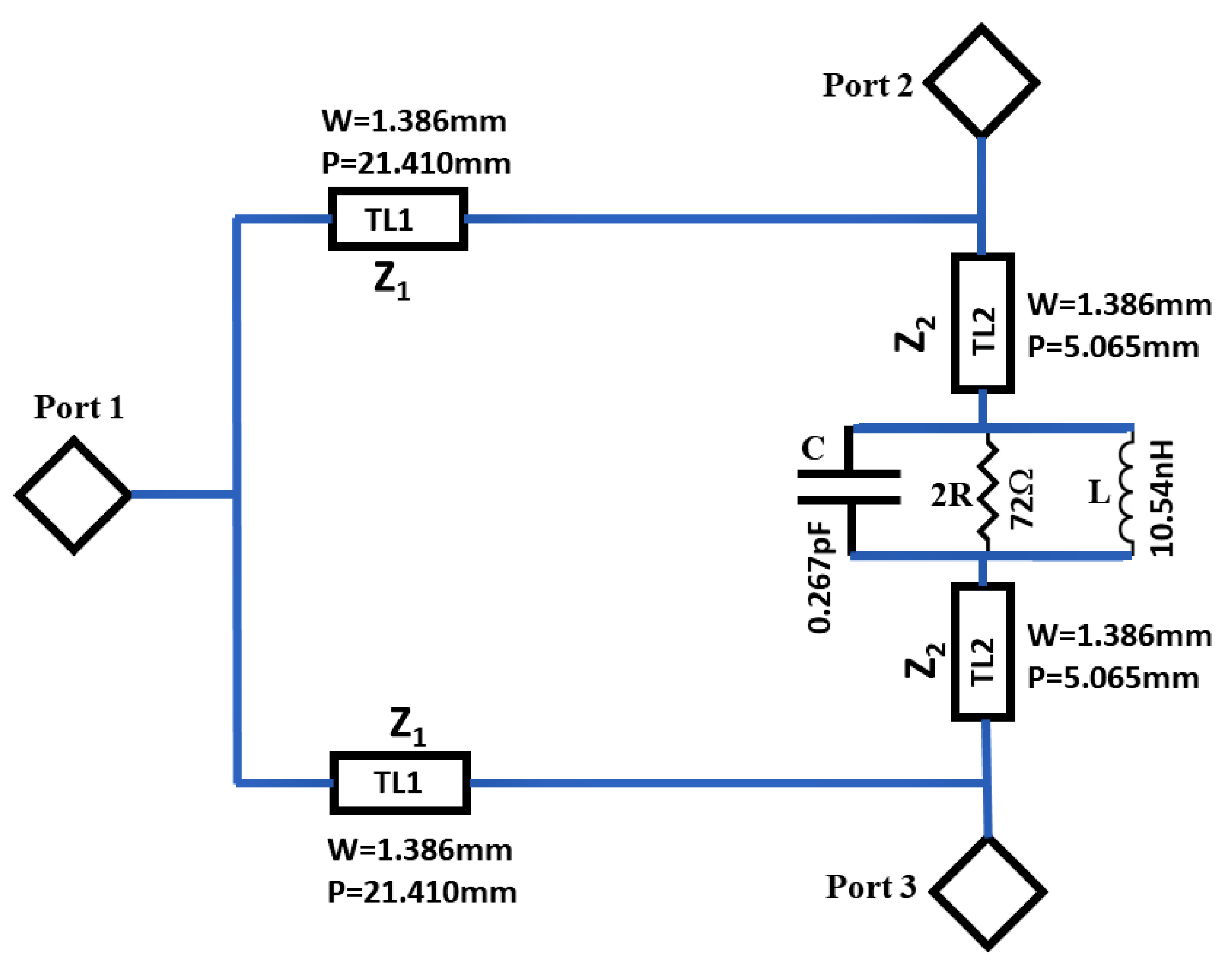
3. Proposed Theory and Design Flow

As the dumbbell-shaped DGS exhibits the properties of a parallel resonant LC circuit, the equivalent circuit of the DGS with an isolation resistor can be depicted (Figure 5). The figure shows that, after incorporating the isolation resistor, the DGS circuit has three paths, i.e., x, y and z via R, L and C, respectively. Thus, the idea is that at the resonant frequency f 0 , paths y and z resist the flow of current. Therefore, these paths demonstrate the characteristic of open circuit and the current will follow the alternative path i.e., path x, which has the resistor across it. Hence, the divider attains maximum isolation due to resistance across path x, as the current faces maximum resistance. Thus, in this way, by introducing DGS in the ground plane and installing the isolation resistor across it, rather than directly mounting it on a top plane of the transmission line, improved isolation can be achieved.
Figure 6a,b shows step-by-step algorithms for the design of the proposed WPD and DGS section, respectively, via flow charts. Although the initial calculated values of parameters will not yield an absolute required result, they pave the way towards obtaining an approximate result. In this way, the variations in the variables of different parameters and their overall effect can be judged and approximated, which leads the way to tune the circuit to achieve the preferable outcome. The steps for the design of the circuit may seem complex and rigorous, but the design flow illustrated in Figure 6a,b can provide an easy and comprehensible way to obtain an acceptable result.

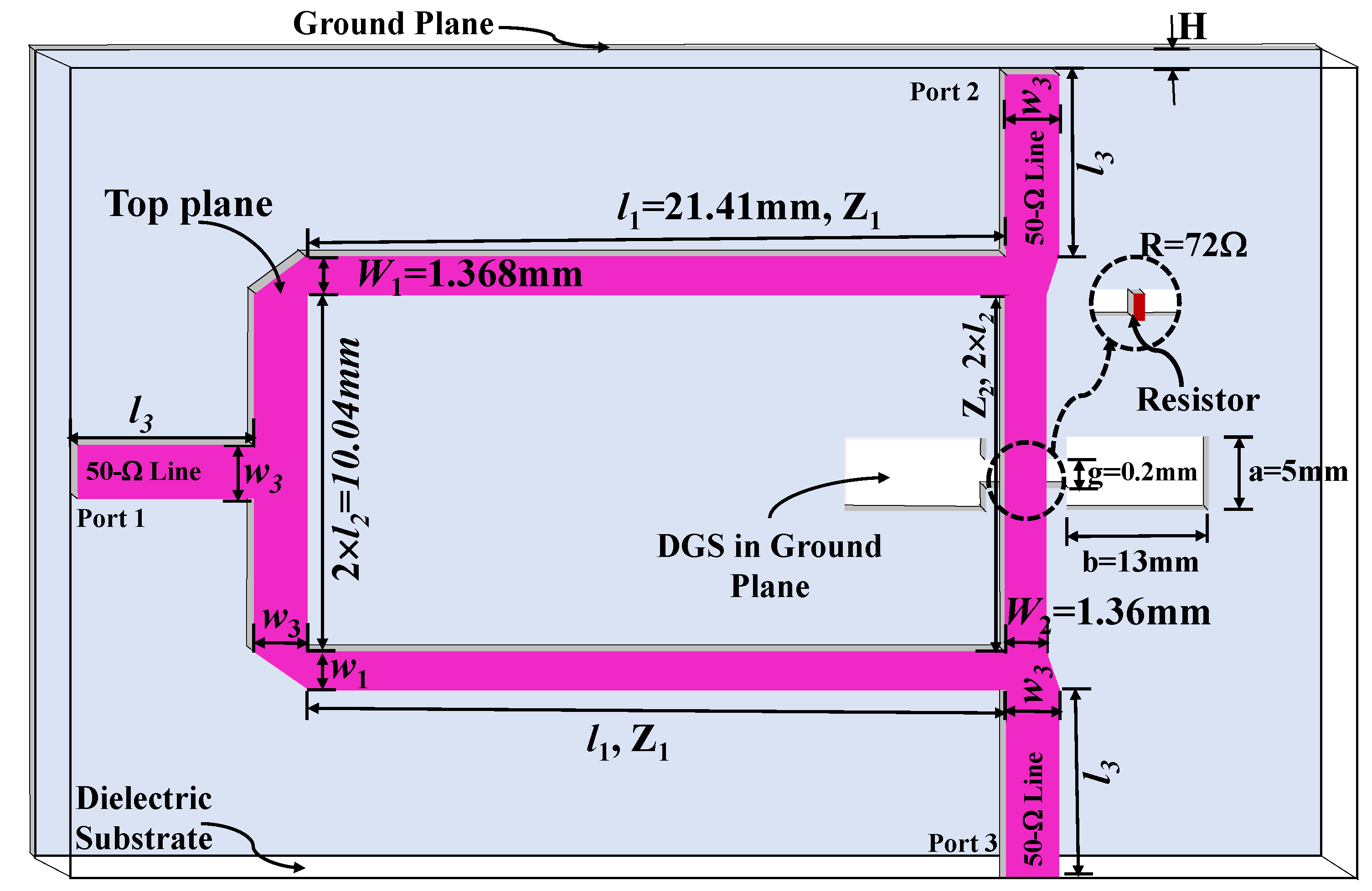
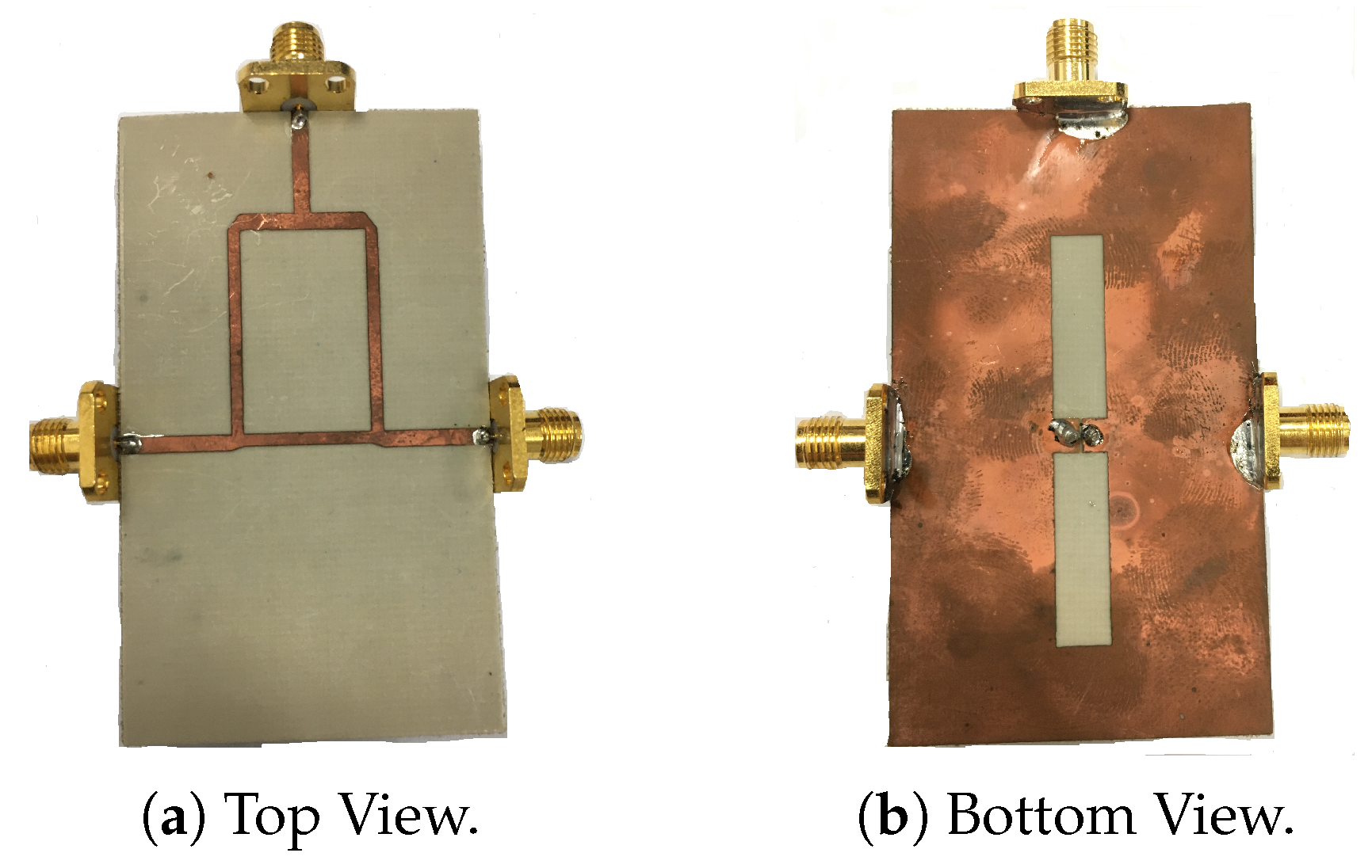
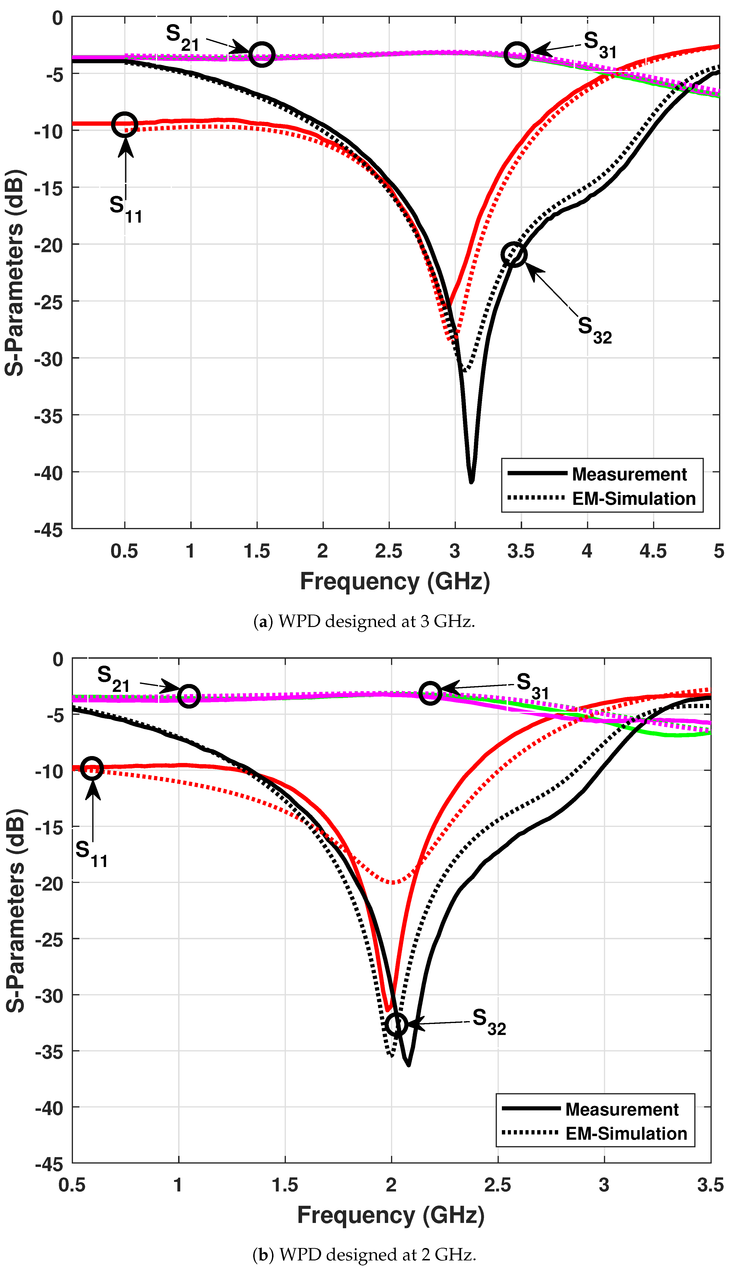
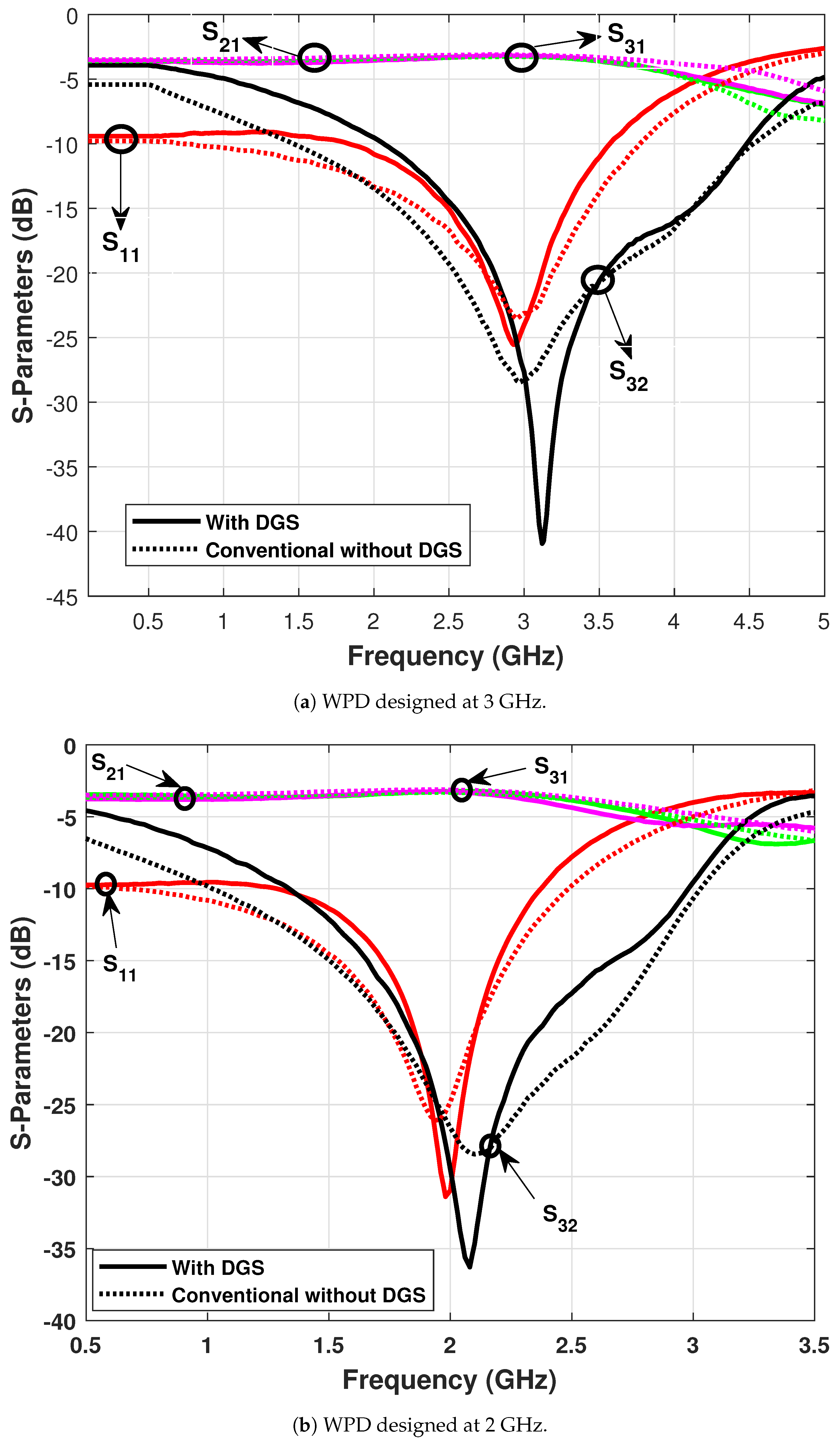
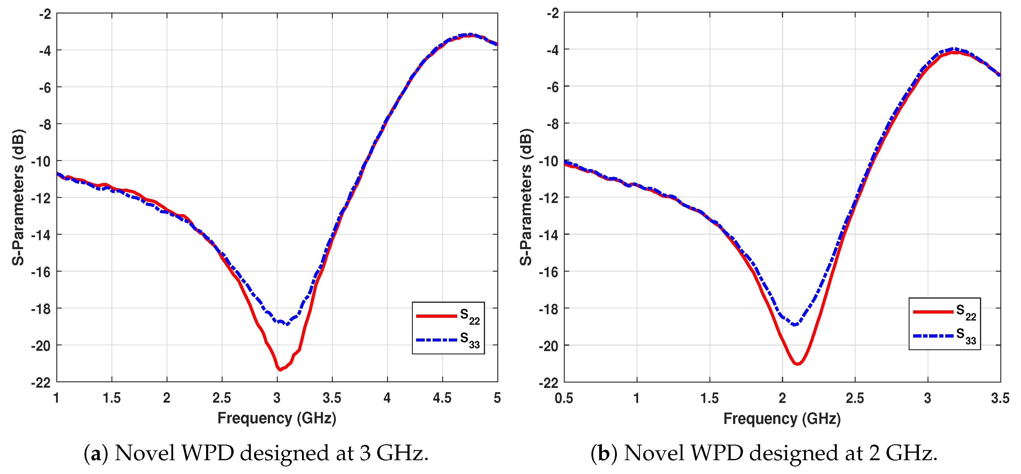
4. Design and Measurement

To demonstrate the proposed design method, two Wilkinson power dividers were designed at the resonant frequencies of 2 and 3 GHz by following the algorithm below, which is illustrated in the flowchart of Figure 6a.
(1)
Draw the proposed WPD circuit and label its essential parameters.
(2)
Apply circuit analysis and conjugate matching theory to extract the required parameters.
(3)
Utilize Microsoft Excel or MATLAB to compose a spreadsheet program or script, in order to calculate the unknown parameters, i.e., θ 1 , θ 2 and isolation resistance R.
(4)
Perform circuit simulation and three-dimensional field analysis using ANSYS Electronics Desktop.
(5)
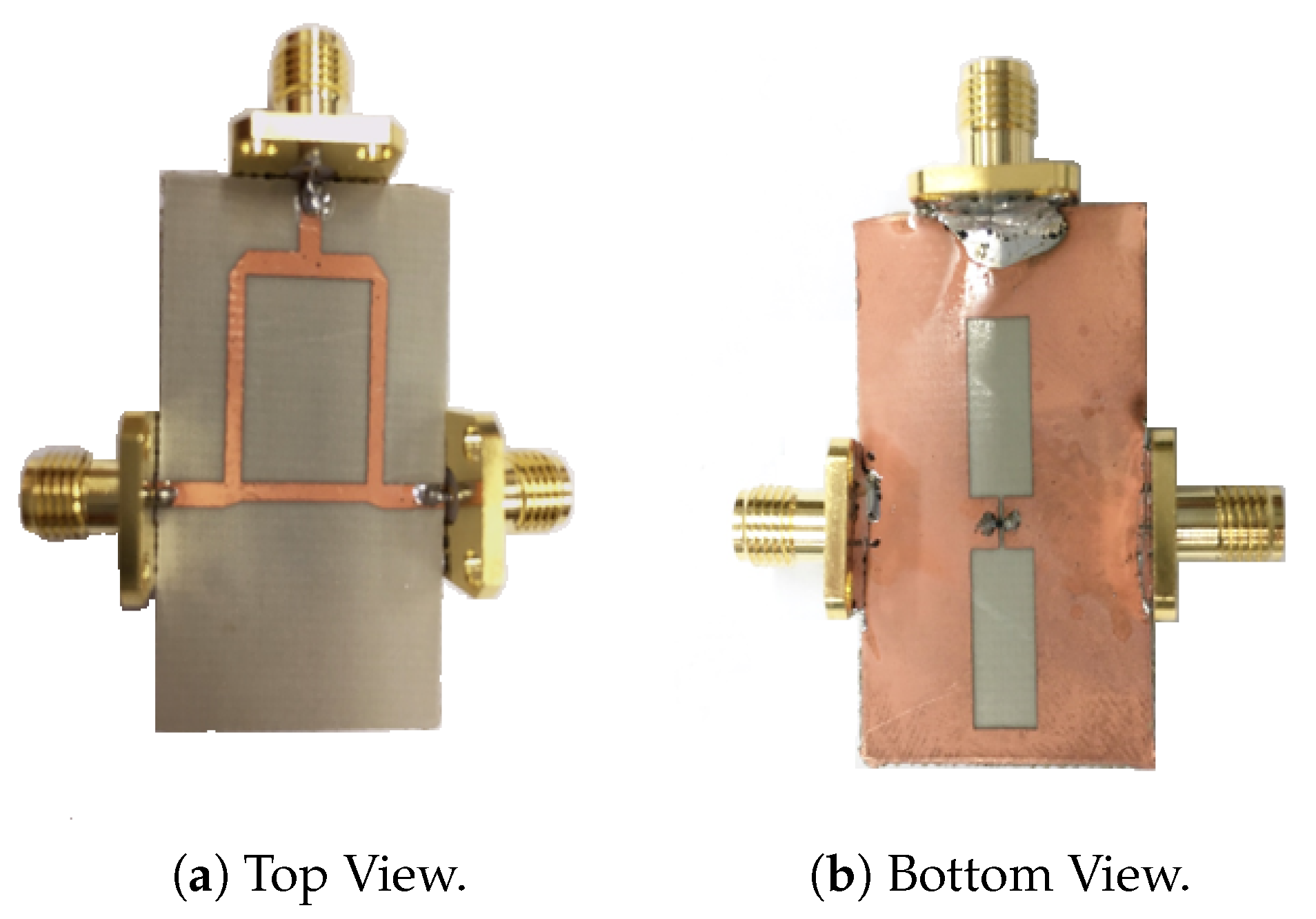
Insert the DGS section into the ground plane utilizing the physical dimensions a, b and g, which are acquired by following the procedure illustrated in Figure 6b, and perform EM simulation.
(6)
If the achieved results are desirable, then fabricate the proposed circuit to check the validity of the circuit.
As the proposed circuit should be viable and compact for fabrication and measurement in order to achieve preferable results, a compromise was made between the availability of the substrate and the compactness of the device as well as the constraints of the fabrication facility. Hence, the impedances of both pairs of transmission lines of the divider, i.e., Z 1 and Z 2 , are fixed at 60 Ω to obtain improved results with the best substrate at hand. Thus, by following the design method given in Figure 6a, the electrical lengths of both transmission lines with impedances Z 1 and Z 2 are calculated. Other parameters are obtained by using ANSYS HFSS via circuit and EM Simulation.
The proposed circuit is simulated with different substrates (available) to examine the performances of substrates and choose the best accessible, available and reliable one which can accommodate the preferred outcome of the proposed WPD. Figure 7 shows that all substrates under test have the capacity to achieve good results with minor variations in return loss and isolation, as shown in Table 1. However, according to the data shown in Table 1, Taconic substrate is well suited for the proposed WPD as it yields better isolation, i.e., S 32 = 55.84 dB, and return loss, i.e., S 11 = 55.02 dB, as compared to other substrates. Furthermore, in the case of FR4 and Rogers, due to low build quality, noise creates signal integrity problems during measurement. Hence, these factors can affect the efficiency and overall performance of the WPD as compared to WPD powered with Taconic substrate.
Therefore, the proposed circuits were simulated and fabricated on a Taconic substrate with a dielectric constant of ε r = 2.97, loss tangent of tan δ = 0.0012 and thickness of H = 0.76 mm. Table 2 shows the calculated optimized values and dimensions of both WPDs.
Therefore, Equations (9), (11) and (14) were plugged into Microsoft Excel or MATLAB by fixing Y 1 and Y 2 , while changing the value of R from 1 to nR, i.e., 1 to 114 Ω . Hence, applying this method, the solution of Equation (14) approached zero when R approached 36 Ω .
The physical dimensions of the DGS cell, i.e., a, b and g, were achieved by following the steps illustrated in Figure 6b:
(1)
Guess the dimensions of the DGS section (trial-and-error method) by taking an approximation from its calculated lumped elements i.e., capacitance and inductance given in Equations (19) and (20).
(2)
Select dielectric material and thickness.
(3)
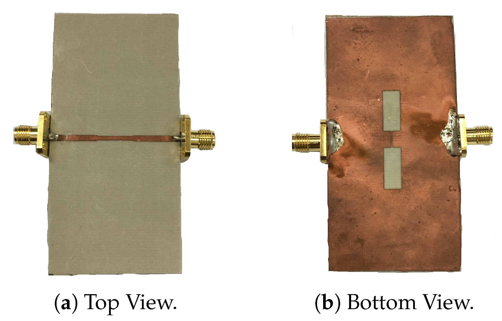
3D simulate the DGS section separately by taking the TL2 line and fabricate the DGS section below the TL2 transmission line.
(4)
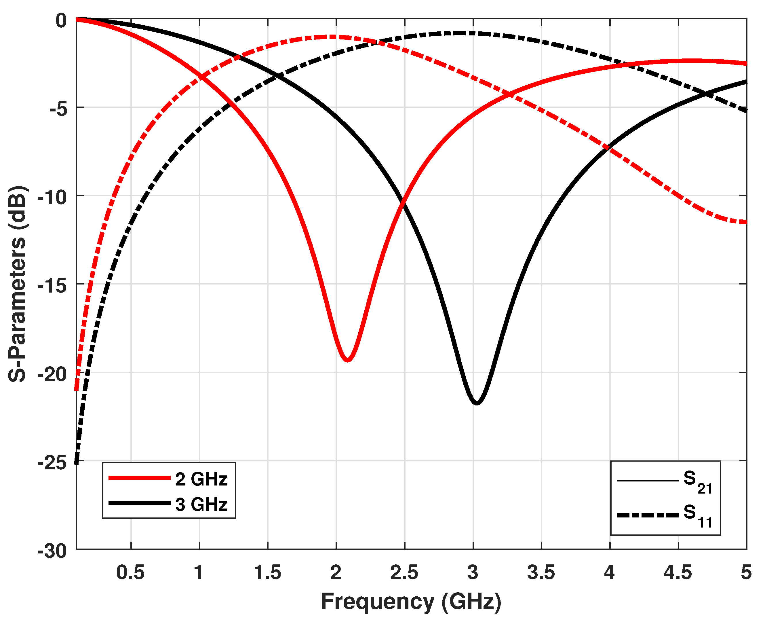
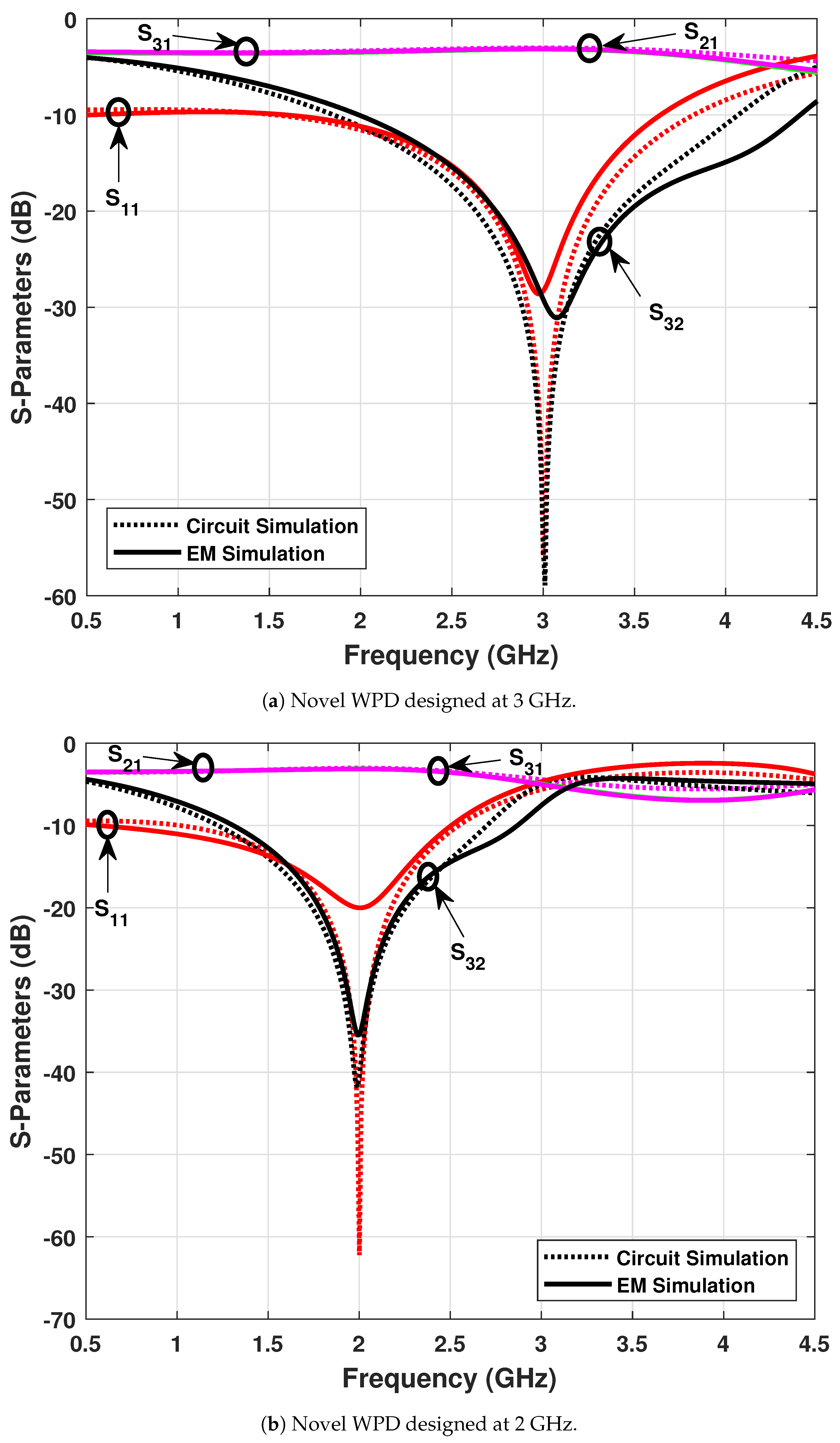
Perform full-wave analysis and extract the S-parameters versus frequency, as shown in Figure 8.
(5)
Change the dimensions of the DGS iteratively, until the frequency response meets the required acceptable result.
(6)
Take the dimensions, i.e., a, b, and g, if the simulated circuit exhibits the required preferable S-parameters, i.e., S 21 at the attenuation pole location is less than −20 dB.
Therefore, to achieve the required parameters of the DGS section, i.e., a, b and g, a separate EM simulation was performed on the transmission line, TL2, of length 2 l 2 , as shown in Figure 9, to get the approximate values of a, b, and g from the preferred results, as shown in Figure 8. Figure 9 shows the photographs of the fabricated one-pole Butterworth low-pass filter designed at 3 GHz with the DGS section under the TL2 microstrip line of length 2 l 2 for the approximation of the physical dimensions of the DGS section. The preferred isolation between Ports 2 and 3 is more than 20 dB, and the proposed WPDs are designed at 3 and 2 GHz. Therefore, to achieve this target, an equivalent low-pass filter with a dumbbell-shaped DGS etched in the ground plane below the transmission line TL2 of length 2 l 2 needs to be designed for each WPD. The dimensions a, b and g of the DGS are changed iteratively until the S 21 is <−20 dB. The preferred S 21 of both WPDs are obtained, as illustrated in Figure 8. The figure shows that the S 21 parameters of both WPDs are in the order of approximately equal to or more than −20 dB. Hence, these results can be taken as adequate reference points for the preferred attenuation poles and the cutoff frequencies. The dimensions a, b and g of the DGS section are obtained from this EM simulation.
To get the parameters of the DGS sections, Figure 8 clearly shows that the resonant frequency or attenuation pole location and cutoff frequency are 3 and 1.5 GHz, respectively, for WPD designed at 3 GHz and 2 and 1 GHz, respectively, for the WPD designed at 2 GHz. Thus, the approximated values of the preferred resonant frequency and cutoff frequency were plugged into Equations (14) and (15) to obtain the values of Capacitance and inductance of an equivalent circuit of the DGS for each divider. To achieve the required cutoff frequency and attenuation pole at a certain frequency, the simulation result should illustrate the characteristics of both low pass and bandstop filter responses simultaneously. To make an effective guess for the initial dimensions of the DGS section, this phenomenon is crucial, i.e., as the etched area, i.e., a × b increases, the cutoff frequency and attenuation pole location move to lower frequencies. Although the variation in the gap distance g results in no change in the cutoff frequency, as the gap distance increases, the location of the attenuation pole shifts to higher frequency [14]. Thus, to attain the preferred result, these approximations are very helpful and are handy to tune and comprehend the best possible effect of each step. The calculated values of the equivalent lumped elements of the equivalent DGS circuits and their respective physical dimensions are shown in Table 3 for both WPDs.
To check the validity of the proposed design technique, ANSYS High Frequency Structure Simulator (HFSS) was used. The design values and dimensions for the proposed circuit are calculated and entered using the values in Table 2, and S-parameter simulation was applied to the proposed circuits. The equivalent LC resonant circuit of the dumbbell-shaped DGS section and the isolation resistor were inserted between the TL2 transmission lines, as shown in Figure 10, to achieve an acceptable isolation.
The circuit simulation was performed by considering and realizing the equivalent lumped elements of the DGS section, as shown in Figure 10. The S-parameters results of the circuit simulations for the proposed circuit, i.e., S 11 , S 21 , S 31 and S 32 , are illustrated as dotted lines in Figure 11a,b, which were designed at 3 and 2 GHz, respectively. It is clear from the results that the designed circuits and their parameters fulfill the requirements for the proposed Wilkinson power dividers, as they achieved good return losses S 11 and isolations S 32 of the order of −55.84 and −55.02 dB, respectively, for the WPD designed at 3 GHz and −60.61 and −40.64 dB, respectively, for the WPD designed at 2 GHz.
ANSYS HFSS Software package (ANSYS Electronics Desktop 2020 R2) was utilized to extract the final layout of the proposed WPD. Figure 11a,b shows the S-parameters results, i.e., S 11 , S 21 , S 31 and S 32 , of an EM simulation for the respective WPDs as solid lines. The calculated values and their respective dimensions are given in Table 2 and Table 3. To achieve an acceptable result, the circuits were tuned slightly. Therefore, the final layouts of the circuits were adjusted slightly, as compared to its initial dimensions. From the simulation results, the proposed circuits achieved almost equal power division, i.e., S 21 S 31 ≈ −3 dB.
Most importantly, they show very good isolations between the output ports, i.e., about S 32 = −29.36 dB and about S 32 = −35.42 dB for the WPDs designed at 3 and 2 GHz, respectively. The results shown in Figure 11a,b also demonstrate good return losses of about S 11 = −28.18 and −20 dB for the WPDs designed at 3 and 2 GHz, respectively. The comparison between the circuit and EM simulation illustrate that the isolation and the return loss are reported to be decreased slightly in case of EM simulation as compared to the results achieved in the circuit simulation. The difference of isolation and return loss are −25.66 and −27.66 dB, respectively, in the case of the WPD designed at the resonant frequency of 3 GHz and approximately −5.22 and −40.61 dB, respectively, in case of the WPD designed at the resonant frequency of 2 GHz.
The proposed Wilkinson power dividers were fabricated on a specified substrate using a special technique called photolithography. Figure 12 and Figure 13 show the pictures of the fabricated circuits designed at the operating frequencies 3 and 2 GHz, respectively.
The simulated (EM simulation) and measured results of both circuits are illustrated in Figure 14 and compared in Table 4. In the case of the measured results, Table 4 shows that, due to attenuation and signal distortion in the microstrip line, the return loss and isolation at the resonating frequencies of 3 and 2 GHz in the fabricated WPDs are decreased to a small degree as compared with the simulation results. The return loss S 11 of the simulated circuit designed at 2 GHz is about −20 dB, which is less preferable. Therefore, the fabricated circuit is tuned slightly by the trial-and-error method to get the preferred measured return loss. Hence, the measured return loss of the divider at 2 GHz is better than the simulated circuit. Moreover, the attenuation pole in both WPDs is shifted slightly to higher frequencies with better dips as compared with the simulation results. Figure 15a,b shows the measured S-parameters results of the fabricated circuits designed at the operating frequencies of 3 and 2 GHz, respectively. Furthermore, conventional WPDs without DGS were also fabricated and compared with the proposed circuits, which are illustrated in Figure 15. Additionally, the measured results of the proposed WPD were compared with conventional WPDs without DGS designed at the same frequencies, i.e., 3 and 2 GHz, as shown in Table 5. Furthermore, the respective parameters, i.e., S 21 , S 31 , S 11 and S 32 , of the proposed circuit and the conventional WPD are compared with other works in Table 5.
Both circuits designed at the resonating frequencies of 2 and 3 GHz are well matched at all ports. Reflection losses, S 22 and S 33 of both WPDs are reported be <−20 dB, which are rather promising results. Figure 16a,b shows the measured S-parameter results, S 22 and S 33 , of the fabricated circuits.
It is clear from the measured results that good agreement is achieved, and the overall results match the required specifications of the proposed Wilkinson power divider. The measured results are approximately identical to the simulated results and have acceptable results. The fabricated circuits designed at resonating frequencies of 3 and 2 GHz have relatively good return losses S 11 of about −25.54 and −31.24 dB, respectively, and achieve good isolations between its output ports, in an order of about S 32 = −40.83 and −36.05 dB within the operating bandwidth, respectively, which is rather exceptional and acceptable. Both Ports 2 and 3 of both dividers achieve approximately equally divided power, i.e., S 31 S 21 ≈ −3 dB. The measured results, i.e., S 11 , S 21 , S 31 and S 32 , of both WPDs designed at operating frequencies of 2 and 3 GHz are illustrated in Table 5.
The improved isolation between the output ports yields good bandwidth for the proposed circuit. Therefore, the calculated operating bandwidths, f H f L (where f H is the higher frequency and f L is the lower frequency of the passband) of the proposed circuit are 0.49 and 0.65 GHz of the WPDs designed at the center frequencies of 2 and 3 GHz, respectively (considering S 11 −15 dB ). The bandwidths of the proposed work are compared with other similar works in Table 5. Table 5 shows comparatively good bandwidths as compared to other works.
The measured results of this work were compared with other similar works as well as with conventional WPDs without DGS. Furthermore, the measured s-parameters results, S 11 , S 21 , S 31 and S 32 , of the conventional WPDs without the DGS were compared with the results of the proposed circuit and other major works. Table 5 shows desirable and improved return loss S 11 and better isolation S 32 results as compared with other major similar works as well as conventional WPDs. In some cases, the proposed work demonstrates better results than other works. Hence, the improved results of the proposed structure show considerable reliability and efficiency. Furthermore, the effective occupied areas of the fabricated WPDs were also compared with other works, as shown in Table 5, which demonstrates comparable or more desired effective areas.

5. Conclusions

In this work, a modified Wilkinson power divider is proposed that has the isolation resistor soldered on the ground plane across an etched dumbbell-shaped DGS. The proposed circuit consists of two pairs of transmission lines having fixed impedances and certain electrical lengths. DGS is introduced between the output ports, such that a resistor can be mounted across the DGS section, in order to achieve better or acceptable isolation. The parameters of the proposed circuit are extracted by applying even and odd mode analysis and conjugate matching theory. Circuit simulation and EM simulation were performed to verify the validity of the proposed circuit and to achieve an acceptable result. This paper also presents the design methodology and the flow charts for both the Wilkinson power divider and the DGS section. The proposed method, parameters and circuit were verified by the fabrication and measurement of modified proposed WPDs circuits designed at the operating frequencies of 2 and 3 GHz. The measured data show approximately equally divided power at the output ports, and improved isolation was achieved between the output ports on both fabricated circuits. The fabricated circuits achieved good return loss characteristics as well. The measured results are acceptable and meet the criteria of the preferred results. An adequate agreement was achieved between the measured performance of the fabricated Wilkinson power divider and the EM simulation results. The measured results were compared with respective conventional WPDs as well as other similar works. The comparisons showed acceptable results with good or better S-parameter results. Furthermore, the results show that the proposed Wilkinson power divider achieved improved isolation as compared to other works.

Author Contributions

Conceptualization, M.S., D.A. and S.-M.H.; methodology, M.S., Y.J. and D.A.; formal analysis, J.L.; data curation, M.S. and Y.J.; writing—original draft preparation, M.S. and Y.J.; writing—review and editing, M.S., and Y.J.; supervision, D.A.; project administration, D.A.; and funding acquisition, D.A. All authors have read and agreed to the published version of the manuscript.

Funding

This research was supported by the MSIT(Ministry of Science and ICT), Korea, under the ICAN(ICT Challenge and Advanced Network of HRD) program(IITP-2021-2020-0-01832) supervised by the IITP(Institute of Information & Communications Technology Planning & Evaluation) and Soonchunhyang University Research Fund.

Institutional Review Board Statement

Not Applicable.

Informed Consent Statement

Not Applicable.

Data Availability Statement

Not Applicable.

Conflicts of Interest

The authors declare no conflict of interest. The funders had no role in the design of the study; in the collection, analyses, or interpretation of data; in the writing of the manuscript, or in the decision to publish the results.

References

  1. Wilkinson, E.J. An N-way hybrid power divider. IRE Trans. Microw. Theory Tech. 1960, 8, 116–118. [Google Scholar] [CrossRef]
  2. Pozar, D.M. Microwave Engineering, 3rd ed.; Wiley: New York, NY, USA, 2005. [Google Scholar]
  3. Lim, J.S.; Park, J.S.; Lee, Y.T.; Ahn, D.; Nam, S. Application of defected ground structure in reducing the size of amplifiers. IEEE Microw. Wirel. Comp. Lett. 2002, 12, 261–263. [Google Scholar]
  4. Sung, Y.J.; Ahn, C.A.; Kim, Y.S. Size reduction and harmonic suppression of rat-race hybrid coupler using defected ground structure. IEEE Microw. Wirel. Comp. Lett. 2004, 14, 7–9. [Google Scholar] [CrossRef]
  5. Woo, D.J.; Lee, T.-K. Suppression of harmonics in Wilkinson power divider using dual-band rejection by asymmetric DGS. IEEE Trans. Microw. Theory Tech. 2005, 53, 2139–2144. [Google Scholar]
  6. Tao, F.; Jun, X.; Yan, W.M. Design of 1:3 unequal Wilkinson power divider with defected ground structure. In Proceedings of the 2010 International Conference on Microwave and Millimeter Wave Technology, Chengdu, China, 8–11 May 2010; pp. 646–648. [Google Scholar]
  7. Lim, J.-S.; Lee, S.-W.; Kim, C.-S.; Park, J.-S.; Ahn, D.; Nam, S. A 4:1 Unequal Wilkinson Power Divider. IEEE Microw. Wirel. Compon. Lett. 2001, 11, 124–126. [Google Scholar]
  8. Kulkarni, M.G.; Sarwade, N. Design analysis and testing of Wilkinson Power Divider with harmonics suppression using Defected Ground Structures. In Proceedings of the 2011 International Conference on Signal Processing, Communication, Computing, and Networking Technologies, Thuckafay, India, 21–22 July 2011; pp. 50–55. [Google Scholar]
  9. Mahouti, P.; Belen, M.A.; Partal, H.P.; Demirel, S.; Günes, F. Miniaturization with the dumbbell-shaped defected ground structure for power divider designs using Sonnet. In Proceedings of the 2015 31st International Review of Progress in Applied Computational Electromagnetics (ACES), Williamsburg, VA, USA, 22–26 March 2015; pp. 1–2. [Google Scholar]
  10. Ahn, D.; Park, J.-S.; Kim, C.-S.; Kim, J.; Qian, Y.; Itoh, T. A design of the low-pass filter using the novel microstrip defected ground structure. IEEE Trans. Microw. Theory Tech. 2001, 49, 86–93. [Google Scholar] [CrossRef]
  11. Yoon, J.-S.; Kim, J.-G.; Park, J.-S.; Park, C.-S.; Lim, J.-B.; Cho, H.-G.; Kang, K.-Y. A new DGS resonator and its application to bandpass filter design. In Proceedings of the 2004 IEEE MTT-S International Microwave Symposium Digest (IEEE Cat. No.04CH37535), Fort Worth, TX, USA, 6–11 June 2004; Volume 3, pp. 1605–1608. [Google Scholar]
  12. Li, J.; Chen, J.; Xue, Q.; Wang, J.; Shao, W.; Xue, L. Compact microstrip lowpass filter based on defected ground structure and compensated microstrip line. In Proceedings of the 2005 IEEE MTT-S International Microwave Symposium Digest, Long Beach, CA, USA, 12–17 June 2005; pp. 1483–1486. [Google Scholar]
  13. Khandelwal, M.K.; Kanaujia, B.K.; Kumar, S. Defected Ground Structure: Fundamentals, Analysis, and Applications in Modern Wireless Trends. Int. J. Antennas Propag. 2017, 2017, 2018527. [Google Scholar] [CrossRef]
  14. Vagner, P.; Kasal, M. Design of microstrip lowpass filter using defected ground structure. In Proceedings of the 2007 17th International Conference Radioelektronika, Brno, Czech Republic, 24–25 April 2007; pp. 1–4. [Google Scholar]
  15. Mirzavand, R.; Honari, M.M.; Abdipour, A.; Moradi, G. Compact Microstrip Wilkinson Power Dividers with Harmonic Suppression and Arbitrary Power Division Ratios. IEEE Trans. Microw. Theory Tech. 2013, 61, 61–68. [Google Scholar] [CrossRef]
  16. Yang, J.; Gu, C.; Wu, W. Design of Novel Compact Coupled Microstrip Power Divider with Harmonic Suppression. IEEE Microw. Wirel. Compon. Lett. 2008, 18, 572–574. [Google Scholar] [CrossRef]
  17. Chongcheawchamnan, M.; Patisang, S.; Krairiksh, M.; Robertson, I.D. Tri-Band Wilkinson Power Divider Using a Three-Section Transmission-Line Transformer. IEEE Microw. Wirel. Compon. Lett. 2006, 16, 452–454. [Google Scholar] [CrossRef]
  18. Ning, J.; Chen, L.; Bu, S.; Zeng, C. A new design of compact microstrip Wilkinson power dividers. In Proceedings of the 2014 IEEE International Symposium on Radio-Frequency Integration Technology, Hefei, China, 27–30 August 2014; pp. 1–3. [Google Scholar] [CrossRef]
  19. Liu, F.-X.; Lee, J.-C. Design of New Dual-Band Wilkinson Power Dividers with Simple Structure and Wide Isolation. IEEE Trans. Microw. Theory Tech. 2019, 67, 3628–3635. [Google Scholar] [CrossRef]
  20. Deepak, V.; Iswariya, S. A Novel Designing and Testing of Two-Way Wilkinson Power Divider. In Proceedings of the 2019 International Conference on Intelligent Sustainable Systems (ICISS), Palladam, India, 21–22 February 2019; pp. 426–430. [Google Scholar] [CrossRef]
  21. Kumar, M.; Islam, S.N.; Sen, G.; Parui, S.K.; Das, S. Design of dual-band Wilkinson power divider using CRLH transmission line based on CSRR. In Proceedings of the 2017 IEEE MTT-S International Microwave and RF Conference (IMaRC), Ahmedabad, India, 11–13 December 2017; pp. 318–321. [Google Scholar] [CrossRef]

Short Biography of Authors

Applsci 11 04148 i001Maaz Salman received his B.S. in Telecommunication and Information System Engineering from University of Engineering and Technology, Pakistan in 2017. He has been pursuing his M.S. in Electrical Communication System Engineering from Soonchunhyang University, Asan, South Korea. Currently, he has been working as Research Assistant at RF and Microwave Components Research Center (RAMREC), Soonchunhyang University, Korea. His research areas include design of passive microwave components, DGS circuit applications and design and simulation of RF front end components at microwave and radio spectrum.
Applsci 11 04148 i002Youna Jang received her master’s degree in electronics and computer engineering from Hanyang University, Seoul, Korea in 2014. She got her Ph.D. in Electrical Communication System Engineering from Soonchunhyang University, Choongnam, Korea in 2019. She participated as a Designer of Duplexer filter in an internship program in 2015 at Qorvo, Bundang, South Korea. She was a lecturer at Soonchunhyang University from 2016 to 2020. She is currently a research professor of Radio and Mechatronics Research Center. Her research areas include the design of passive components in microwave band.
Applsci 11 04148 i003Jongsik Lim received the B.S. and M.S. degrees in Electronic Engineering from Sogang University in Seoul, Republic of Korea in 1991 and 1993, and Ph.D. degree in the School of Electrical Engineering and Computer Science from Seoul National University in 2003. In 1993, he joined Electronics and Telecommunications Research Institute (ETRI) and worked in the Satellite Communications Division as a senior member of research staff. From March to July in 2003, he worked in Division of Information Technology, Brain Korea 21 Project in Seoul National University as a post doctoral fellow. He has experiences as a patent examiner in the Korean Intellectual Property Office (KIPO) through July 2003 to September 2004. Since March 2005, he has been with the Department of Electrical Engineering, Soonchunhyang University in Asan, Chungnam, Korea, as a professor. His current research interests include design of the passive and active circuits for RF/microwave and millimeter-wave with MIC/MMIC technology, modeling of active device, design of high-power amplifiers for mobile communications, applications of periodic structure to the RF/microwave circuits and modeling of passive structure having periodic structures. Prof. Lim is a senior member of IEEE, and member of IEICE (the Institute of Electronics, Information and Communication Engineers, Japan) and KIEES (Korea Institute of Electromagnetic Engineering and Science).
Applsci 11 04148 i004Dal Ahn received the B.S., M.S., and Ph.D. degrees from Sogang University, Seoul, Korea, in 1984, 1986, and 1990, respectively, all in electronics. From 1990 to 1992, he was with the Mobile Communications Division, Electronics and Telecommunications Research Institute (ETRI), Daejeon, Korea. Since 1992, he has been with the School of Electrical and Electronic Engineering, Soonchunhyang University, Asan, Chungnam, Korea, where he is currently a Professor. He is also currently Chief of the RF and Microwave Component Research Center (RAMREC), Soonchunhyang University. He is also a Technical Consultant for Tel Wave Inc., Suwon, Korea. His current research interests include the design and application of passive and active components at radio and microwave frequencies, design of the RF front-end module for various handset system using low-temperature co-fired ceramic (LTCC) technology, DGS circuit applications, and circuit modeling using a commercial EM analysis program. He is an Editor of the Journal of Korea Electromagnetic Engineering Society. Prof. Ahn is a senior member of the Korea Electromagnetic Engineering Society (KEES).
Applsci 11 04148 i005Sang-Min Han received the B.S., M.S., and Ph.D. degrees in radio sciences and engineering from Korea University, Seoul, Korea, in 1996, 1998, and 2003, respectively. From 1999 to 2001, he was a Lecturer with the School of Electrical Engineering, Korea University. From 2003 to 2004, he was a Post–Doctoral Research Fellow with the University of California at Los Angeles (UCLA), U.S. From 2005 to 2007, he was a Senior Research Engineer with the Samsung Advanced Institute of Technology (SAIT), Korea. In 2007, he joined Soonchunhyang University, Korea where he is a Professor with the Department of Information and Communication Engineering. He was a Visiting Research Faculty with Georgia Institute of Technology (GT), Atlanta, U.S. from 2013 to 2014. Prof. Han is an Associate Editor of the Journal of the Korean Institute of Information Technology (JKIIT) and an Editorial Board Member of the Journal of Electromagnetic Engineering and Science (JEES). He appears in Marquis’ Who’s Who in Science and Engineering (2006–2007) and Marquis’ Who’s Who in Asia (2007). His research interests include RF/microwave system architectures with low-power/spectrum sensing, active integrated antennas, and reconfigurable RF systems/components.
Figure 1. Three-dimensional view of the proposed Wilkinson Power Divider (WPD) at the operating frequency of 3 GHz with the DGS section etched in the ground plane.
Applsci 11 04148 g001
Figure 2. Proposed WPD circuit with λ / 4 transmission lines of characteristic impedances of Z 1 and Z 2 , respectively.
Applsci 11 04148 g002
Figure 3. Even and odd mode Analysis of the proposed circuit.
Applsci 11 04148 g003
Figure 4. Equivalent circuits of one-pole Butterworth-type low-pass filter and DGS.
Applsci 11 04148 g004
Figure 5. Dumbbell-shaped DGS section between the transmission lines TL2 with its equivalent lumped elements and physical dimensions.
Applsci 11 04148 g005
Figure 6. Design flow of the proposed circuit.
Applsci 11 04148 g006
Figure 7. Simulated S–parameters results of the proposed circuit with different substrates.
Applsci 11 04148 g007
Figure 8. Simulated S–parameters results of the DGS sections for the approximation of the physical dimensions.
Applsci 11 04148 g008
Figure 9. Photographs of the fabricated one-pole Butterworth low-pass filter designed at 3 GHz with the DGS section under the transmission line of the length 2 l 2 for the approximation of the physical dimensions a, b and g of the DGS section.
Applsci 11 04148 g009
Figure 10. Circuit schematic analysis of WPD designed at 3 GHz with physical dimensions and equivalent DGS circuit.
Applsci 11 04148 g010
Figure 11. Simulation results of the proposed WPD circuit.
Applsci 11 04148 g011
Figure 12. Photographs of the fabricated WPD circuit designed at 3 GHz.
Applsci 11 04148 g012
Figure 13. Photographs of the fabricated WPD circuit designed at 2 GHz.
Applsci 11 04148 g013
Figure 14. Simulated and measured S–parameters results of the proposed WPDs.
Applsci 11 04148 g014
Figure 15. MeasuredS–parameters results of the fabricated conventional WPDs and the proposed WPDs with DGS.
Applsci 11 04148 g015
Figure 16. Measured S–parameter results ( S 22 , S 33 ) of the proposed WPD circuits.
Applsci 11 04148 g016
Table 1. Circuit simulation results of the proposed WPD designed at 3 GHz with different substrates.
Substrate ε r H
(mm)
S 11
(dB)
S 32
(dB)
Bandwidth
(GHz)
Rogers RO30066.151−43.55−46.360.56
FR44.41−38.98−38.210.57
Taconic2.970.76−55.02−55.840.56
Table 2. Calculated design parameters using the proposed method ( ε r = 2.97, H = 0.76 mm, R = 36   Ω ).
ParameterImpedance
Z
(Ω)
Electrical
Length
( θ )
Physical
Width
(mm)
Physical
Length
(mm)
TL1:3GHz Z 1 = 60 θ 1 = 117.88 w 1 = 1.368 l 1 = 21.41
TL2:3GHz Z 2 = 60 θ 2 = 27.88 w 2 = 1.368 l 2 = 5.065
TL1:2GHz Z 1 = 60 θ 1 = 117.88 w 1 = 1.368 l 1 = 32.16
TL2:2GHz Z 2 = 60 θ 2 = 27.88 w 2 = 1.368 l 2 = 7.606
50 Ω Line Z 0 = 50- w 3 = 1.8707 l 3 = 13.699
Table 3. Lumped values and physical dimensions of DGS sections ( ε r = 2.97, H = 0.76 mm).
Operating
Frequency
C
(pF)
L
(nH)
a
(mm)
b
(mm)
g
(mm)
3 GHz0.26710.545130.2
2 GHz0.378916.716210.2
Table 4. Comparisons of S-parameters at the resonating frequencies of 2 and 3 GHz of the simulated and fabricated circuits.
Operating Frequency (GHz)Return Loss
S 11
(dB)
Isolation
S 32
(dB)
Coupling
S 21
dB
Coupling
S 31
dB
3Simulated−28.18−29.36−3.12−3.17
Measured−24.01−27.65−3.23−3.24
Error (±dB)−4.17−1.71−0.11−0.07
2Simulated−20−35.42−3.13−3.13
Measured−30.95−29.53−3.24−3.30
Error (±dB)10.95−5.89−0.11−0.17
Table 5. Comparison of fabricated WPDs’ results with other major similar works.
Operating
Frequency
(GHz)
Return Loss
S 11
(dB)
Isolation
S 32
(dB)
Coupling
S 21
(dB)
Coupling
S 31
(dB)
Occupied
Effective Area
l × w
(mm2)
Bandwidth
f H f L
(GHz)
[15]1−27.9−30−3.34−3.31 21 × 18 0.27
[16]0.9> 30 −23≈−3≈−3 12.9 × 13.6 0.43
[17]2.43> 26 > 20 55 × 31 0.1
[18]0.8> 20 27 16 × 18 0.12
[19]3.5 25 25.9 −3.32−3.37 54.8 × 22.36 0.24
[20]0.46> 20 33.5 −3.261−3.242 40.5 × 20.9 0.3
[21]2.9 23 31 −3.8−3.74 19.37 × 19.8 0.14
C2−24.81−26.62−3.32−3.14 22.15 × 15.2 1.2
C3−27.66−25.37−2.91−2.90 15.9 × 8 1.8
*2−31.24−36.05−3.24−3.30 23.3 × 12 0.49
*3−25.54−40.83−3.23−3.24 14.9 × 8.12 0.65
C: Conventional WPD; *: This work.
Publisher’s Note: MDPI stays neutral with regard to jurisdictional claims in published maps and institutional affiliations.

