Featured Application
The geometric degrees of freedom of additive manufacturing and the high temperature performance of ceramic materials open up new areas of application such as aerospace or automotive disruptives.
Abstract
Ceramic materials are chemical- and temperature-resistant and, therefore, enable novel application fields ranging from automotive to aerospace. With this in mind, this contribution focuses on developing an additive manufacturing approach for 3D-printed waveguides made of ceramic materials. In particular, a special design approach for ceramic waveguides, which introduces non-radiating slots into the waveguides sidewalls, and a customized metallization process, are presented. The developed process allows for using conventional stereolithographic desktop-grade 3D-printers. The proposed approach has, therefore, benefits such as low-cost fabrication, moderate handling effort and independence of the concrete waveguide geometry. The performance of a manufactured ceramic WR12 waveguide is compared to a commercial waveguide and a conventionally printed counterpart. For that reason, relevant properties, such as surface roughness and waveguide geometry, are characterized. Parsing the electrical measurements, the ceramic waveguide specimen features an attenuation coefficient of 30–60 dB/m within the E-Band. The measured attenuation coefficient is 200% and 300% higher compared to the epoxy resin and the commercial waveguide and is attributed to the increased surface roughness of the ceramic substrate.
1. Introduction
In passive systems for higher frequency ranges above 20 GHz, waveguide technology offers several major advantages over printed circuit boards (PCBs) which are limited to a planar structure by their nature. While small cross-section microstrip lines exhibit relatively high conductor loss scaling in a fashion with frequency, inevitable dielectric loss resulting from the PCB substrate comes on top scaling even in a direct proportionality with frequency [1]. Conductor surface roughness () further increases conductor loss effects while at the same time also generating an impact on the phase behavior [2,3,4].
Both loss mechanisms are addressed by hollow waveguides. The larger cross-section allows for a reduction in conductor losses, while the absence of lossy laminate material makes dielectric losses negligible. Passive components suhc as waveguide circuits [5], compact couplers [6], horn antennae [7,8] or slotted waveguide array (SWA) antennae [9,10] can be realized in waveguide technology.
However, those systems are typically rather bulky and weighty due to their full metal nature and conventional manufacturing of such includes expensive micro machining, high precision milling and assembly. In addition, the complexity of manufacturing increases disproportionately with increasing system complexity.
The latter drawbacks could be successfully addressed and overcome by novel additive manufacturing (AM) methods including polymer-based 3D printing, such as digital light processing (DLP) [11] or stereolithography (SLA) [12], and a subsequent metallization process. By making use of the slotted waveguide approach, where non-radiating slots are introduced into the narrow walls of the waveguide, printing and metallization qualities can be enhanced, enabling the fabrication of even relatively complex structures for millimeter-wave (mmWave) frequency range, such as waveguides, or waveguide paths for E- [13,14] and D-band [15], hybrid couplers for both bands [16,17,18], W-band SWAs [19], helix antennae for 77 GHz [20] that can be used in imaging applications [21], wavemode transitions [22,23] and even entire six-ports from one monolithic model [24].
All those components are made of photopolymer epoxy resins, which offer advantages such as low weight, low surface roughness (typ. 1 µm) and a well established plating process. However, those materials have low thermal stability up to 80–300 °C and poor chemical resistance. Moreover, their suitability for vacuum environments, such as space applications, has not yet been proven.
Hence, there is a potential demand for materials that overcome those challenges while at the same time being printable, lightweight and, therefore, meeting the requirements imposed by passive mmWave systems.
Ceramic materials offer excellent high-temperature properties, are chemically stable and can be used in vacuum environments [25,26]. Therefore, they are well suited for the desired applications. In current research, various AM approaches for ceramic materials have been proposed. For example, in [27,28,29], fused deposition modeling (FDM) was applied by using polymer-based composite materials. By mixing ceramic fillers into a resin, various ceramic materials can be produced by SLA and DLP [30,31,32,33,34]. Recent progress in robocasting as described, e.g., in [35], allows for direct writing of ceramic materials. Compared to FDM, SLA and robocasting, DLP enables an almost free design customization, a printing of detailed structures and a short curing time [31] and is, therefore, especially attractive for fabrication of complex structures, such as waveguide geometries.
However, AM of ceramic materials has, so far, not been applied to the fabrication of waveguides and systems for mmWave applications. Therefore, this contribution introduces an AM concept and design guidelines for producing ceramic waveguides and waveguide systems.
The contribution is organized as follows: The next section describes the novel AM process. Section 3 summarizes and discusses the measurement results. Ultimately, the fabricated waveguides are characterized optically (Section 3.1) and electrically (Section 3.2).
2. Manufacturing Process
The manufacturing process for a ceramic waveguide can be separated into four different steps. In a first step (Section 2.1), the geometry of the waveguide is prepared and modified in order to enable an AM process. Then, the waveguide is fabricated by a DLP printer (Section 2.2) before it is sintered (Section 2.3) and finally metallized (Section 2.4).
2.1. Design for Manufacturing
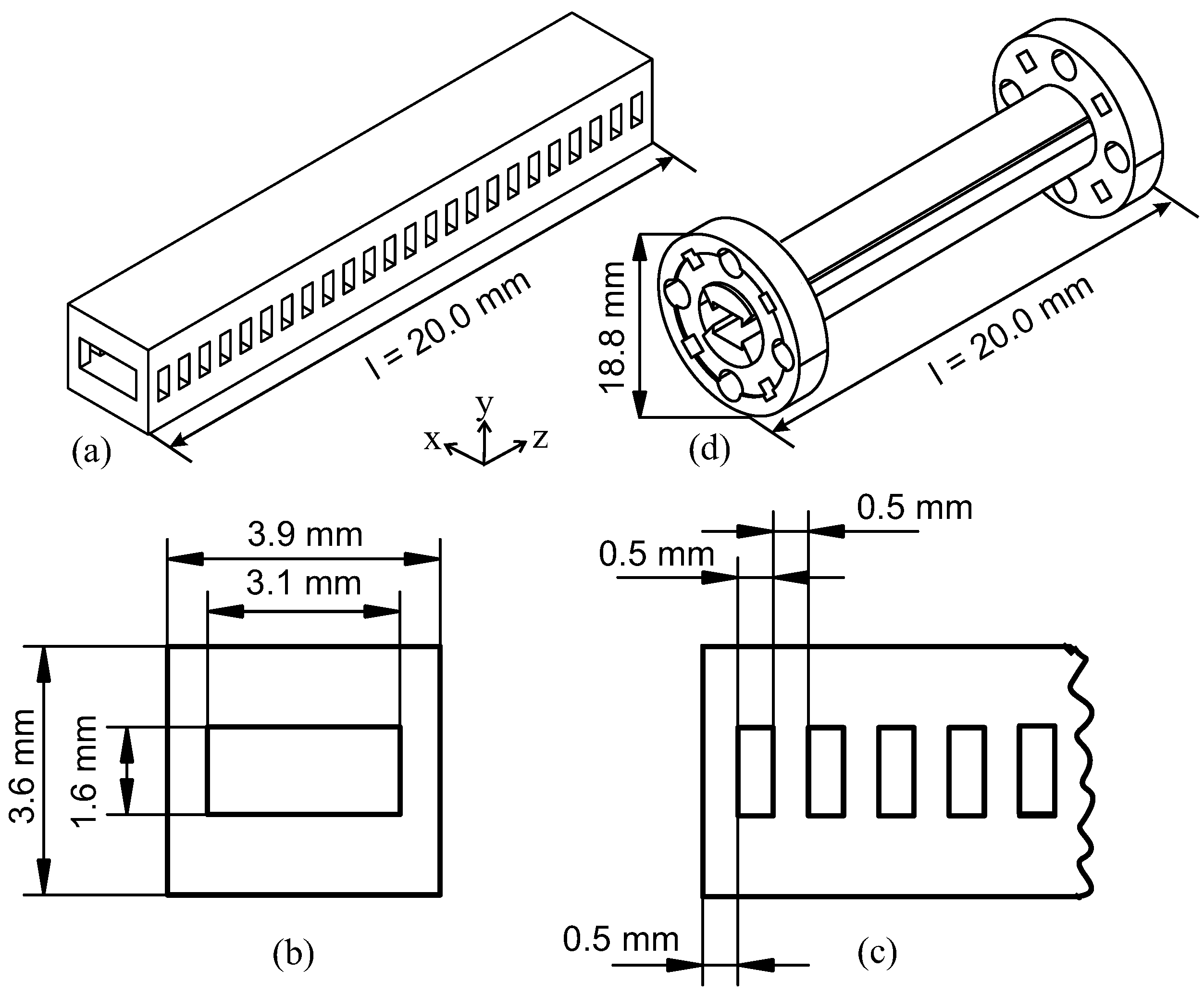
In order to enable an AM process, the standard geometry, exhibiting completely enclosed sidewalls, of a WR12 waveguide was slightly modified to improve subsequent post-processing and the metallization processes. Therefore, non-radiating slots were inserted in the side walls as pointed out in Figure 1a–c. The slots are oriented parallel to the direction of the current density and thus do not affect the spatial field distribution. The slot dimensions were already optimized in previous works of the authors [14]. In order to provide a mounting to a vector network analyzer (VNA) with E-Band converters, the waveguides (Figure 1a–c) can be inserted in a fixture (Figure 1d) which provides additional flanges.
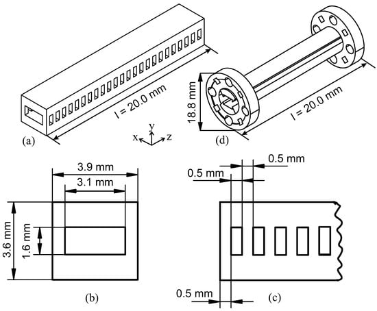
Figure 1.
CAD model (a–c) of the proposed WR12 waveguide. The waveguide in (a–c) can be mounted in an additional fixture (d) which provides flanges for measurements with a VNA.
2.2. Printing Process
To produce the desired components, a so-called DLP printer was used. DLP is a resin-based printing process in which an ultraviolet (UV) sensitive resin (photopolymer) is cured layer by layer by irradiating it with light [11,12]. The process was developd to 3D print polymers, but if ceramic powder is added to the resin, ceramics can also be produced using this process. After printing, the samples were heat-treated, the resin was burnt out (debinded) and the ceramic sintered to the desired component. The choice of the ceramic material is critical for the printing as well as the sintering process. In this work, a low temperature cofired ceramic powder (Ferro® L5) was used, which has a suitable -particle size of 2.65 µm [36] and can be mixed well with the resin (Tethon3D® Gensis). The resulting glass-ceramic provides sufficient temperature resistance for the desired application scenario with simultaneous low sintering temperature, which simplifies the fabrication. The samples were sintered in a laboratory furnace (Nabertherm® LE 14/11/P300) at 900 °C.
A powder-resin mixture was prepared. The rheological properties of the powder-resin mixture are a crucial parameter for the 3D-printing process [31,37,38,39]. Higher mixing rations enable a better loading content. However, a lower mixing ratio leads to a lower viscosity and allows for a better printing performance. Therefore, different mixing ratios (30 wt% (weight percent powder content), 40 wt%, 50 wt%) were examined in a previous parameter study. A mixing ratio of 40 wt% ceramic powder enabled the best printing quality. Before printing, the viscosity of the resin and the ceramic filled resin was measured, and the results are shown in Section 3.
Before printing, this mixture was degassed in order to remove air bubbles, which would otherwise lead to defects in the component. The printing process was then performed using a conventional desktop-grade DLP printer (Elegoo® Mars 2 Pro). The layer thickness was set to 0.01 mm. Each layer was photo cured for six seconds under a light intensity of 8.5 mW/cm2 at 405 nm wavelength.
2.3. Debinding and Sintering Process
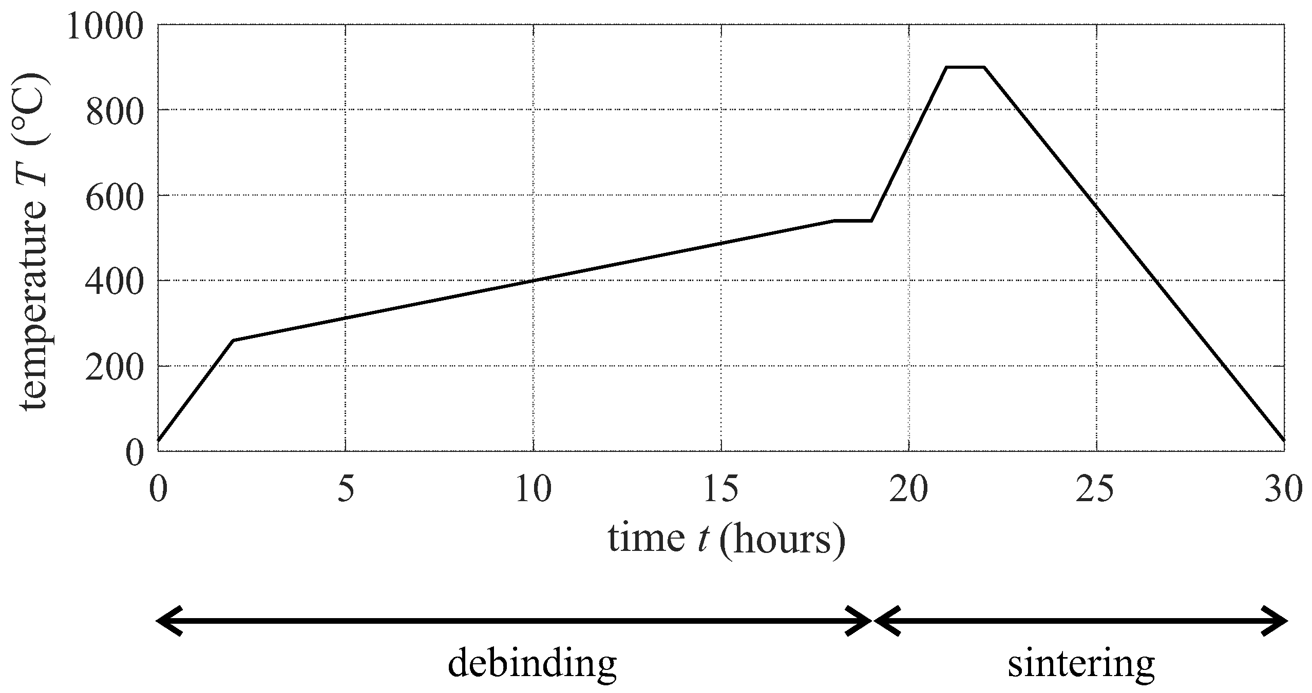
Prior to sintering, a debinding step was performed to remove the residual photopolymer (Figure 2). For this purpose, a heating rate of 0.3 K/min at 260 °C was applied. In order to prevent oxidation reactions, the debinding was performed in flowing nitrogen atmosphere. Following the debinding, the sintering was performed at 540 °C with a heating rate of 3 K/min. Afterward, the waveguides were slowly cooled to room temperature (cooling rate 1.8 K/min).

Figure 2.
Temperature profile of the debinding and sintering process.
2.4. Metallization Process
After the sintering processes, the surface of the waveguide was coated by a conductive layer. Before, contaminations were removed by a polar agent (e.g., dichloromethan). Since used ceramic material is acid-resistant, conventional metallization approaches, such as electroless silver plating [14,15], etc., are difficult in application. Therefore a novel, patent pending approach, as described in [40], was used. The ceramic waveguide was dipped in a silver nanoparticle ink and subsequently heat-treated in order to activate the ink. Afterward, an additional copper layer was applied by electroplating. The dipping as well as the electroplating process benefits from the gaps in the waveguides sidewalls.
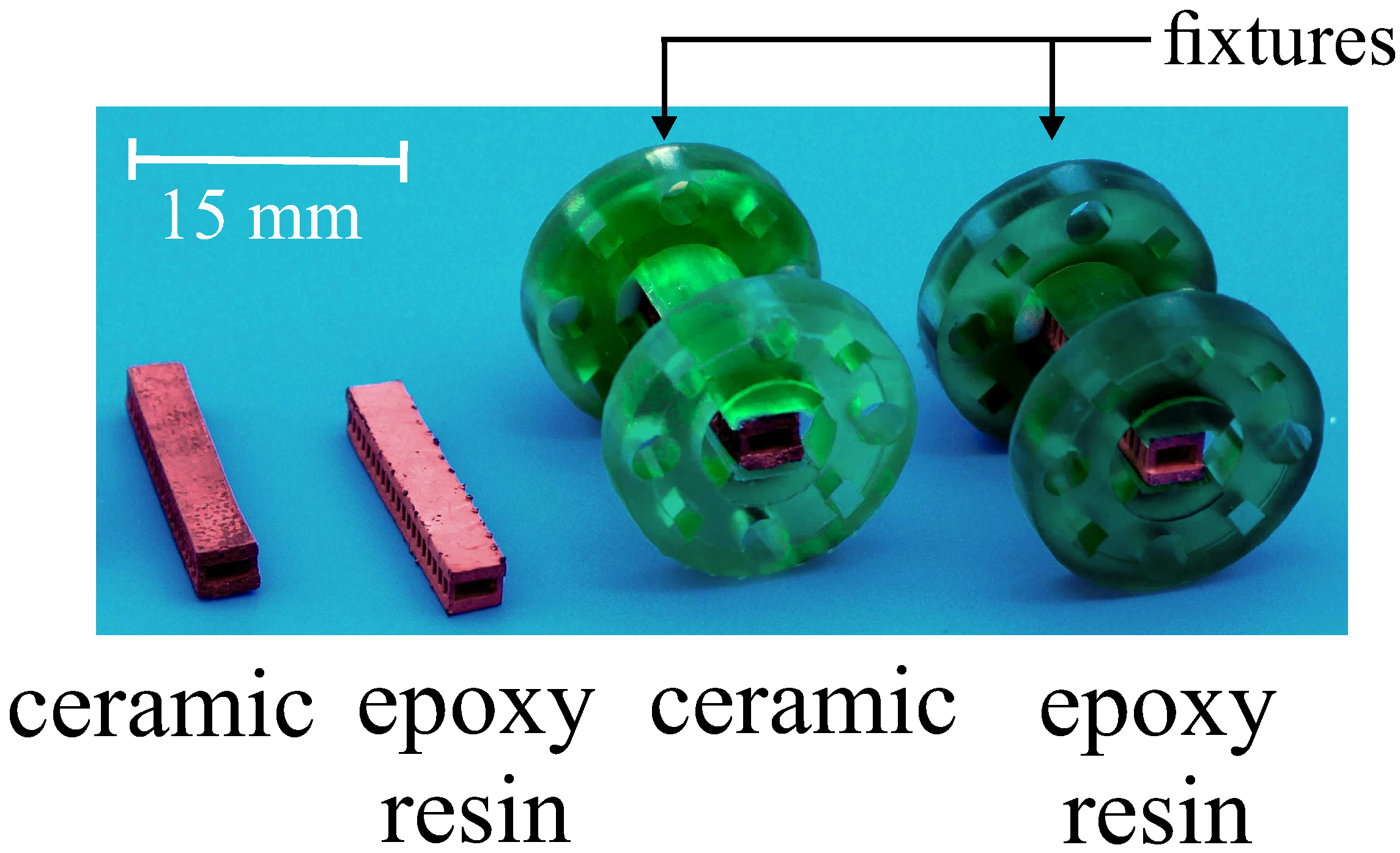
An image comparing the fabricated ceramic waveguide with a waveguide of the same dimensions printed by a conventional epoxy resin [14] is shown in Figure 3. Both specimens feature the same metallization process for reasons of comparability. To enable mounting on conventional measurement equipment, both waveguides can be placed in an additional DLP-printed fixture.
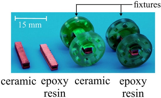
Figure 3.
Photography of the different prototypes with (right) and without (left) fixtures for mounting purposes.
3. Results and Discussion
3.1. Characterization of the Ceramic Filled Resin and the Printed Structures
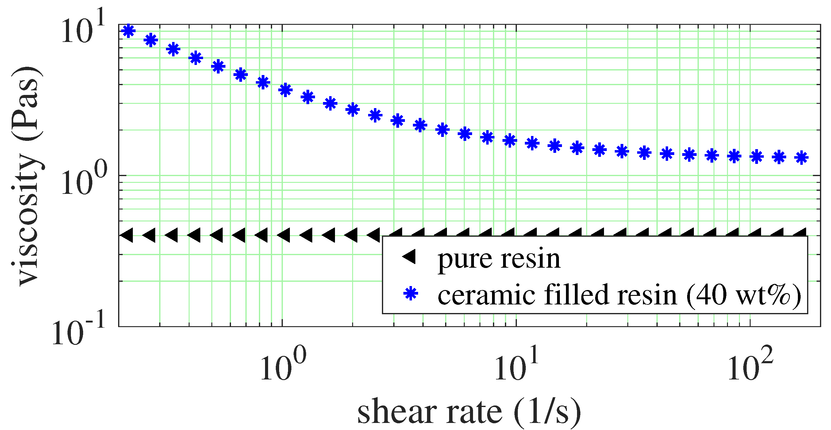
The rheology of the resin, as well as the ceramic filled resin, which is a crucial parameter for the printing process, was measured using a stress-controlled viscometer (Anton Paar® MCR 302) at 20 °C. The viscosity of the pure resin as well as the ceramic filled resin (with 40 wt% powder content) was investigated at shear rates ranging from 0.2 to 500 1/s (Figure 4). The pure resin shows a Newtonian behavior, whereas the ceramic filled resin shows a shear-thinning behavior which is desirable for the printing process. The high viscosity at low shear rates results in good stability of the suspension and prevents the ceramic powder from sedimentation. At higher shear rates, the resin flows more easily, which is advantageous for the printing process. The viscosity settles at a value of about 1.5 Pas, which corresponds to the specifications in the literature (≤3 Pas) and thus enables good printability [31,33,39,41].
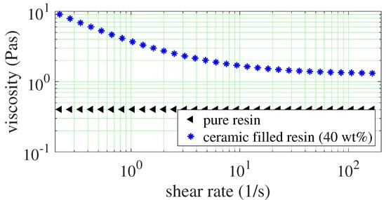
Figure 4.
Measured viscosity of the pure resin and the ceramic filled resin (with 40 wt% powder content).
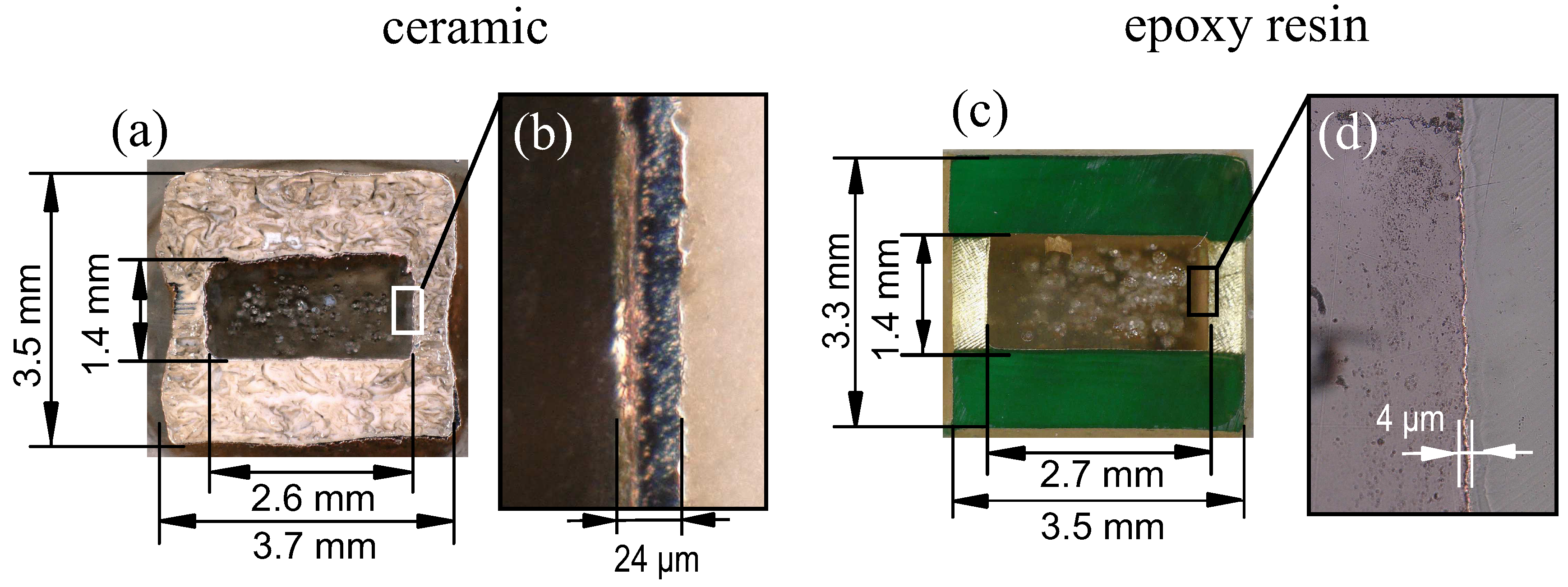
The geometrical accuracy of the manufactured prototypes have a critical influence on their high-frequency performance. In particular, deviations of the waveguides’ width and height [1,42], the position of the slots [14] as well as the surface roughness, surface impedance and surface texture [8,43] can lead to deterioration of the wave propagation. The mechanical properties were, therefore, characterized using a surface microscope (Keyence® VK-X1100) and a scanning electron microscope (SEM, FEI Ltd.® Quanta 200). In order to compare the mechanical properties with the state of the art, the ceramic waveguide was also compared to a waveguide made from epoxy resin (Figure 3) using the DLP method with the same printer. The outer geometry of this waveguide was adapted to the geometry of the sintered ceramic waveguide for sake of comparability.
In Figure 5, polished cross-sections of the ceramic and the epoxy waveguides are shown. On the surface of the samples, the metal layer is clearly visible. Due to the sintering process, the ceramic sample features significant deviations and irregularities from the target geometry (Figure 1). However, the ceramic waveguide features a higher thickness of the metal layer and, therefore, a lower surface impedance. The higher roughness of the ceramic waveguide surface allows a better adhesion during the metallization process.
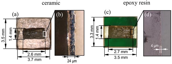
Figure 5.
Polished cross-sections of a ceramic (a,b) and epoxy resin printed (c,d) WR12 waveguide.
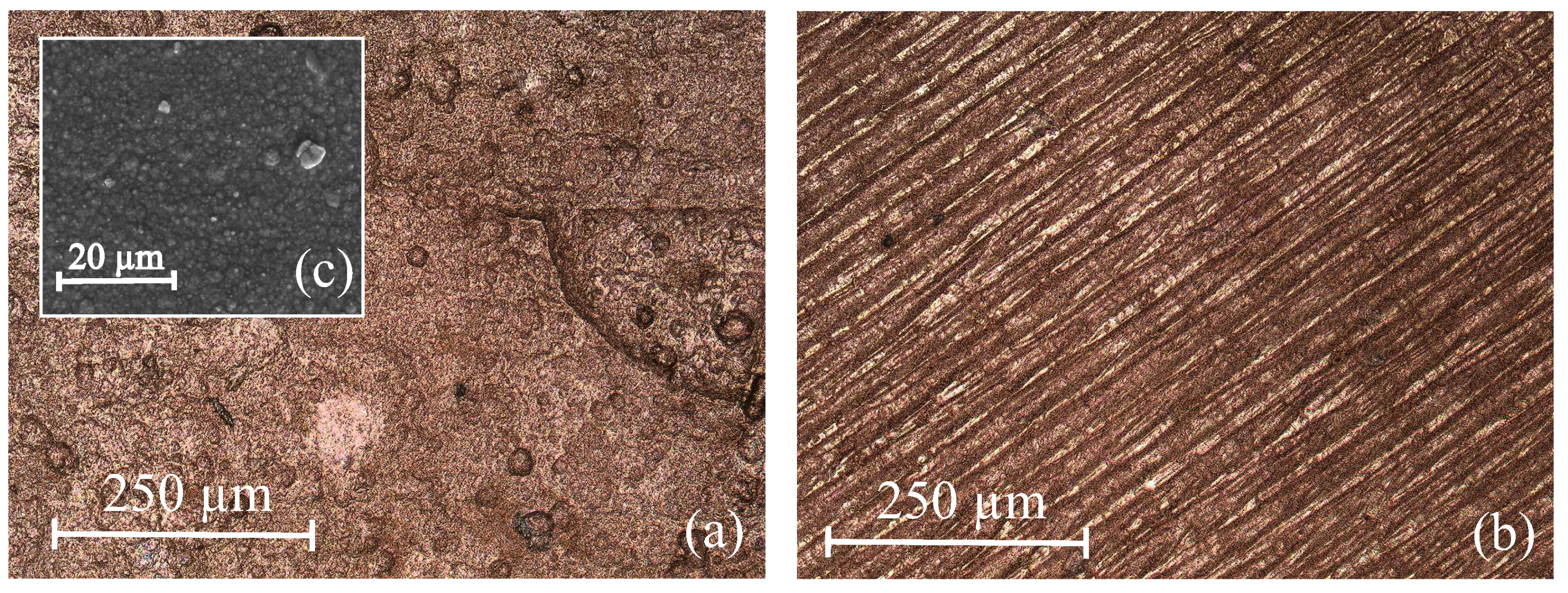
The surface roughness of the metallic layer has a significant influence on the electrical loss mechanism within the waveguide [8,43]. Therefore, the surface roughness on the inside of the waveguides was determined with the surface microscope (Figure 6) by evaluating the root mean square of the surface profile. Due to the large grain size of the ceramic powder (-particle size 2.65 µm), the ceramic waveguide has a significantly higher surface roughness ( 2.43 µm) compared to the epoxy resin-based substrate ( 0.53 µm). As a result of the better surface quality of the epoxy resin-based waveguide, the layers of the DLP printing process appear in its close-up view (Figure 6b). Furthermore, the surface of the ceramic waveguide has significant inhomogeneities due to the different particle sizes of the ceramic powder used. In order to characterize the surface roughness in more detail, SEM images were taken from the inside of the ceramic waveguide (Figure 6c).
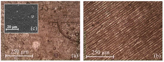
Figure 6.
Close-up view of the inner surfaces of the fabricated waveguides. Compared to the standard printing approach with epoxy resin (b), the ceramic waveguide (a,c) features a higher surface roughness (epoxy resin: 0.53 µm, ceramic: 2.43 µm).
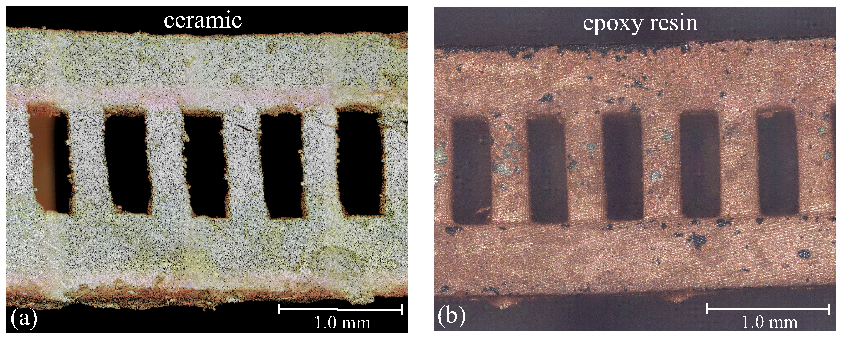
However, when comparing the geometry of the printed samples (Figure 7) and not just the surface quality, it is clear to see that both samples are comparable and do not deviate much from the CAD file (Figure 1). Considering five printed waveguides and comparing their geometric dimensions, the ceramic waveguides feature a dimensional accuracy of ±0.05 mm in the xy-plane and ±0.3 mm in z-direction. The epoxy resin printed waveguides feature a dimensional accuracy of ±0.02 mm in the xy-plane and ±0.1 mm in z-direction, respectively. The obtained parameters are, therefore, within the specifications of the used DLP-printer (xy-resolution: 0.05 mm, z-axis accuracy: 0.2 mm) [44].
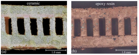
Figure 7.
Close-up view of the narrow walls of the fabricated ceramic WR12 waveguide (a) in comparison to the standard printing approach with epoxy resin (b). The slot geometries are almost identical.
3.2. Electrical Characterization
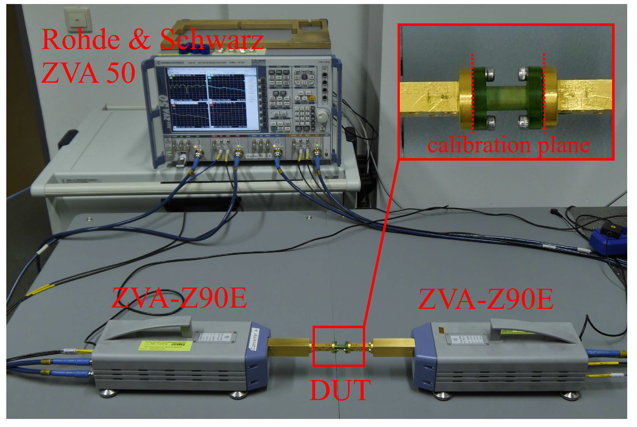
The measurement setup to determine the high-frequency performance of the fabricated waveguides is depicted in Figure 8. By using a VNA (Rohde & Schwarz® ZVA 50) with E-band frequency converters (Rohde & Schwarz® ZVA Z90E), the scattering parameters were obtained and the results are shown in Figure 9. The reference planes were calibrated to the flange-interfaces of the frequency converters by a TOSM (Through, Offset-Short, Short, Match) calibration algorithm with waveguide calibration standards. Based on the scattering parameters, the attenuation coefficients of the different samples can be calculated according to
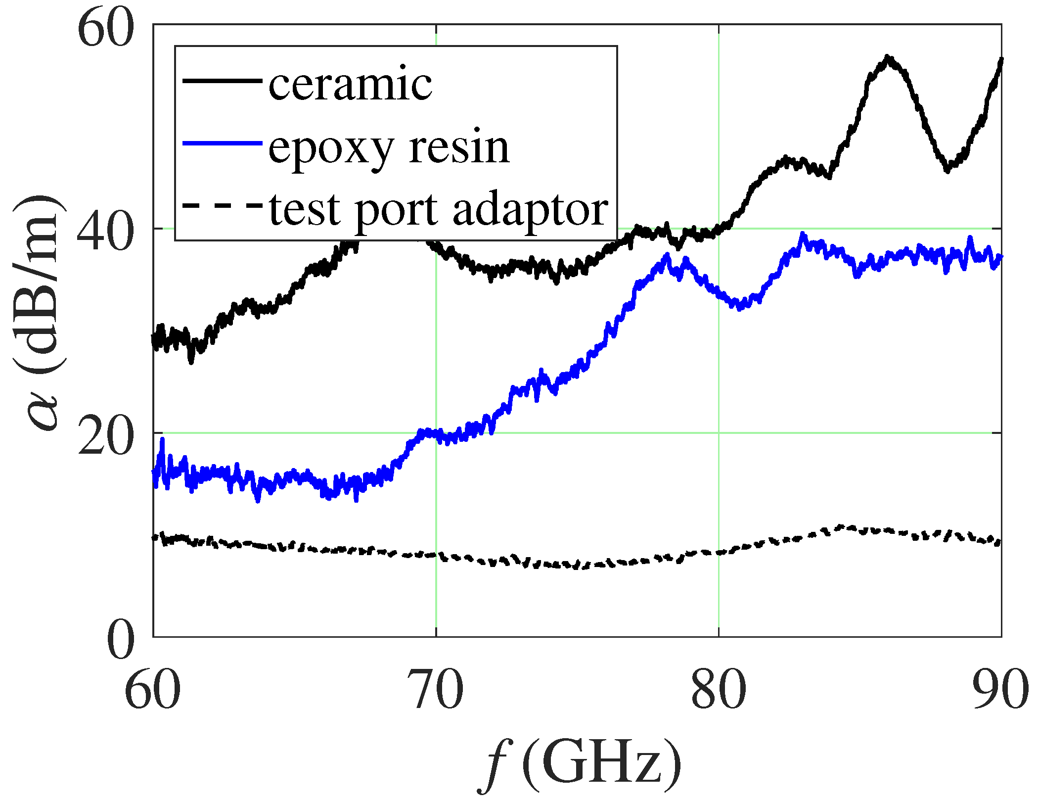
whereby l corresponds to the length of the device under test. In order to give a comparison to a conventionally fabricated waveguide, a commercial WR12 test port adaptor (Rohde & Schwarz® HP/A) is used as a reference and is additionally shown in Figure 10. Due to the higher surface roughness and smaller waveguide cross-section (both height and width), the epoxy resin and ceramic waveguide feature a higher attenuation compared to the test port adaptor. However, geometry deformation is a major contribution to the relativity high attenuation which would (in case of a straight, non-deformed waveguide) exhibit similar attenuation levels as the test port adaptor as shown in [14,23]. The additional attenuation, which is introduced by the ceramic waveguide, compared to the epoxy resin-based one, stems from the additional surface roughness ( 2.43 µm vs. 0.53 µm).

Figure 8.
Photography of the measurement setup for determining the scattering parameters of the fabricated waveguides.
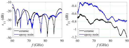
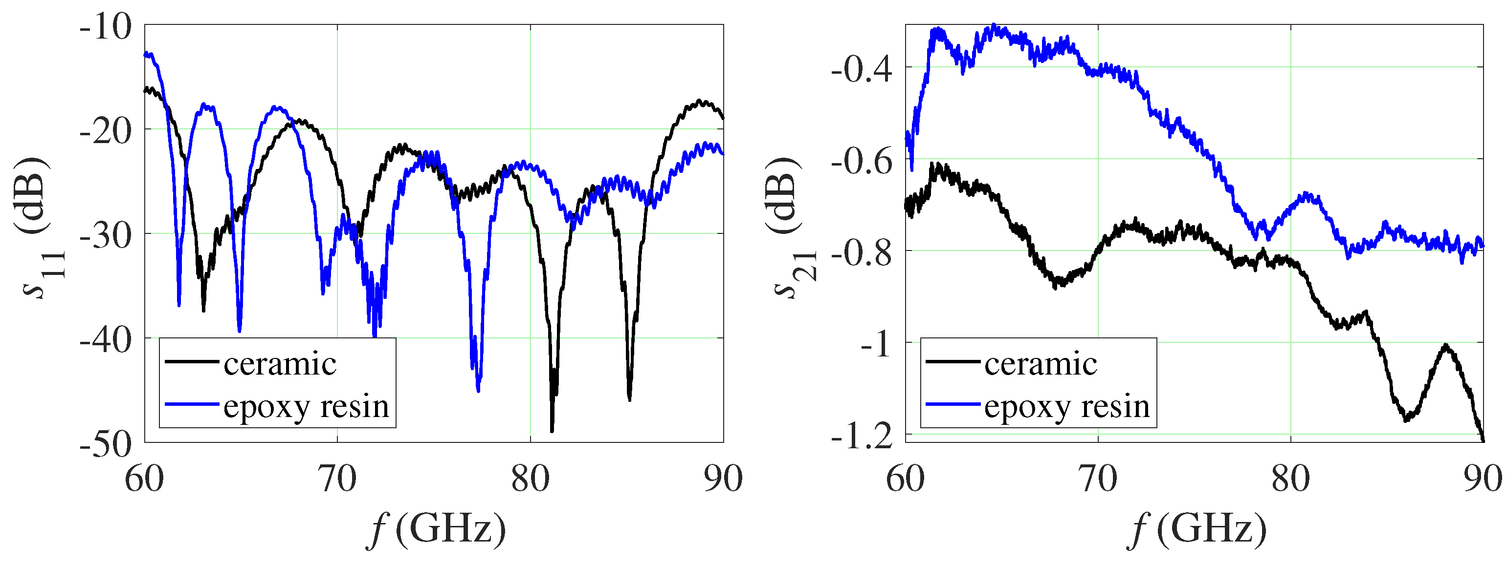
Figure 9.
Measured return loss and insertion loss of the fabricated WR12 waveguides.
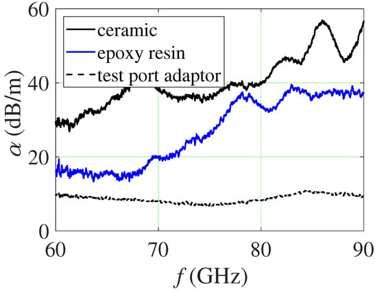
Figure 10.
Measured attenuation coefficient of the fabricated WR12 waveguides compared to a test port adaptor.
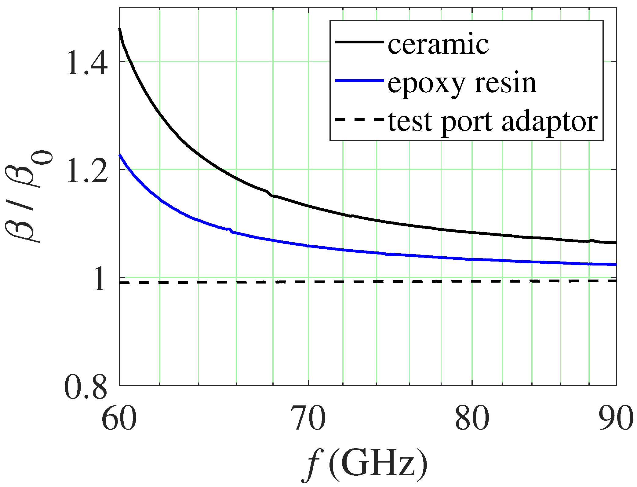
The measured normalized phase coefficient [42] in Figure 11 still exhibits the typical waveguide behavior but indicates significant deviations in geometry, which can be seen, for example, in the shift of the cutoff frequency. was calculated from the ideal dimensions of a WR12 waveguide as stated in [1]. The test port adaptor exhibits a -ratio near one, since its dimensions are very close to an ideal WR12 waveguide. As already pointed out in Section 3.1, the epoxy resin prototype was adapted to the geometry deformations of the ceramic specimen and, therefore, includes the impact of irregularities along the propagation direction. However, the ceramic pendant still shows a higher deviation from , indicating deviations of its cross-section along the propagation direction.
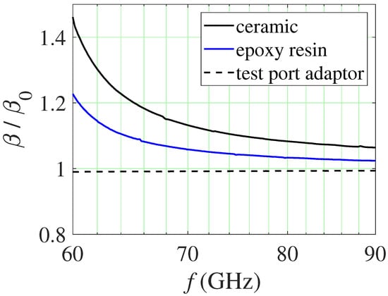
Figure 11.
Measured normalized propagation constant of the fabricated WR12 waveguides compared to a test port adaptor.
Therefore, the suitability of the novel AM process is clearly demonstrated. It can be stated that the geometric distortion due to the subsequent processes, i.e., debinding and sintering, is most critical for reproducible manufacturing of waveguide components.
4. Conclusions
This contribution introduced a novel additive manufacturing approach for waveguide interconnects in mmWave-range. Using ceramic materials as a base body, introducing non-radiating slots in the waveguide sidewalls and applying a customized metallization process enables the fabrication of temperature- and chemical-resistant high-frequency devices. The proposed manufacturing process utilizes a standard desktop-grade DLP printer and allows a cost-efficient rapid-prototyping process. To the best of the authors’ knowledge, in this work the first ceramic-based slotted waveguide fabricated by AM was shown.
The ceramic filled resin and the manufactured WR12 waveguide were characterized. In our measurements, the ceramic filled resin showed a shear-thinning behavior which enabled good printability. The printed waveguides were optically characterized by a surface and a scanning electron microscope and featured a surface roughness of 2.43 µm. In the electrical characterization, an attenuation coefficient of 30–60 dB/m within the E-Band was achieved. This relatively large attenuation coefficient, compared to conventionally manufactured waveguides, is due to the high surface roughness of the ceramic body as well as its geometric inhomogeneities. If these disadvantages are redressed, there is a novel additive manufacturing process for high-frequency applications where polymer-based substrates cannot be used due to thermal limitations.
Therefore, our future work will go towards using ceramic powders with smaller particle diameter, using professional SLA-printers for ceramics and optimization of the sintering process regarding minimal spatial warping.
Author Contributions
Conceptualization, F.H., K.L. and G.G.; methodology, F.H., T.B. and K.L.; software, T.B., A.H. and K.L.; validation, F.H., T.B., A.H., K.L. and M.S.; formal analysis, F.H., T.B., L.W., K.L. and G.G.; investigation, F.H., T.B. and K.L.; resources, F.H., L.W., N.T., K.L. and M.S.; data curation, F.H., T.B. and K.L.; writing—original draft preparation, F.H., L.W. and K.L.; writing—review and editing, F.H., T.B., L.W., A.H., K.L., M.S., N.T. and G.G.; visualization, F.H.; supervision, F.H. and K.L.; project administration, M.S., K.L. and G.G.; funding acquisition, M.S., K.L. and G.G. All authors have read and agreed to the published version of the manuscript.
Funding
This research was funded by the EXIST Transfer of Research Program of the German Federal Ministry for Economic Affairs and Energy, grant number 03EGSFQBY244.
Institutional Review Board Statement
Not applicable.
Informed Consent Statement
Not applicable.
Data Availability Statement
The data presented in this study are available on request from the authors.
Acknowledgments
The authors would like to thank Ferro Corporation, Mayfield Heights, Ohio, U.S.A. and Ute Bollert, Department Elektrotechnik-Elektronik-Informationstechnik, Friedrich-Alexander-Universität Erlangen-Nürnberg, Germany for providing the samples and technical assistance.
Conflicts of Interest
The authors declare no conflict of interest.
Abbreviations
The following abbreviations are used in this manuscript:
| AM | Additive manufacturing |
| CAD | Computer-aided design |
| DLP | Digital light processing |
| FDM | Fused deposition modeling |
| mmWave | Millimeter-wave |
| PCB | Printed circuit board |
| SEM | Scanning electron microscope |
| SLA | Stereolithography |
| SWA | Slotted waveguide array |
| UV | Ultraviolet |
| VNA | Vector network analyzer |
References
- Pozar, D.M. Microwave Engineering; Wiley: Hoboken, NJ, USA, 2012; Volume 4. [Google Scholar]
- Gold, G.; Helmreich, K. A physical model for skin effect in rough surfaces. In Proceedings of the 2012 7th European Microwave Integrated Circuit Conference, Amsterdam, The Netherlands, 29–30 October 2012; pp. 631–634. [Google Scholar]
- Gold, G.; Helmreich, K. A Physical Surface Roughness Model and Its Applications. IEEE Trans. Microw. Theory Technol. 2017, 65, 1–13. [Google Scholar] [CrossRef]
- Gold, G.; Lomakin, K.; Helmreich, K.; Arz, U. High-Frequency Modeling of Coplanar Waveguides Including Surface Roughness. Adv. Radio Sci. 2019, 17, 51–57. [Google Scholar] [CrossRef]
- Bruneau, P.J.; Janzen, H.D.; Ward, J.S. Machining of terahertz split-block waveguides with micrometer precision. In Proceedings of the 2008 33rd International Conference on Infrared, Millimeter and Terahertz Waves, Pasadena, CA, USA, 15–19 September 2008; pp. 1–2. [Google Scholar] [CrossRef]
- Cano, J.L.; Ceccato, G.; Fernandez, T.; Mediavilla, A.; Perregrini, L. An Ultra-Compact Full-Band Waveguide Quadrature Hybrid Coupler. IEEE Microw. Wirel. Compon. Lett. 2021, 1–4. [Google Scholar] [CrossRef]
- Sadiq, M.S.; Niaz, M.W.; Zheng, S.; Zhao, L. Equal Beamwidth and Low Sidelobe mm-Wave Horn Antenna. In Proceedings of the 2018 Asia-Pacific Microwave Conference (APMC), Kyoto, Japan, 6–9 November 2018; pp. 1579–1581. [Google Scholar] [CrossRef]
- Lomakin, K.; Pavlenko, T.; Sippel, M.; Gold, G.; Helmreich, K.; Ankenbrand, M.; Urban, N.; Franke, J. Impact of surface roughness on 3D printed SLS horn antennas. In Proceedings of the 12th European Conference on Antennas and Propagation (EuCAP 2018), London, UK, 9–13 April 2018; pp. 1–4. [Google Scholar] [CrossRef]
- Tyagi, Y.; Mevada, P.; Chakrabarty, S.; Jyoti, R. High-Efficiency Broadband Slotted Waveguide Array Antenna. IET Microw. Antennas Propag. 2017, 11, 1401–1408. [Google Scholar] [CrossRef]
- Misilmani, H.M.E.; Al-Husseini, M.; Kabalan, K.Y. A Design Procedure for Slotted Waveguide Antennas with Specified Sidelobe Levels. In Proceedings of the International Conference on High Performance Computing and Simulation, Bologna, Italy, 21–25 July 2014. [Google Scholar]
- Pagac, M.; Hajnys, J.; Ma, Q.P.; Jancar, L.; Jansa, J.; Stefek, P.; Mesicek, J. A Review of Vat Photopolymerization Technology: Materials, Applications, Challenges, and Future Trends of 3D Printing. Polymers 2021, 13, 598. [Google Scholar] [CrossRef]
- Huang, J.; Qin, Q.; Wang, J. A Review of Stereolithography: Processes and Systems. Processes 2020, 8, 1138. [Google Scholar] [CrossRef]
- Lomakin, K.; Herold, S.; Simon, D.; Sippel, M.; Sion, A.; Vossiek, M.; Helmreich, K.; Gold, G. 3D Printed Slotted Rectangular Hollow Waveguides. In Proceedings of the 2019 IEEE MTT-S International Microwave Symposium, Boston, MA, USA, 2–7 June 2019. [Google Scholar]
- Lomakin, K.; Herold, S.; Ringel, L.; Ringel, J.; Simon, D.; Sippel, M.; Sion, A.; Vossiek, M.; Helmreich, K.; Gold, G. SLA Printed 3D Waveguide Paths for E-Band using Electroless Silver Plating. IEEE Trans. Compon. Packag. Manuf. Technol. 2019, 9, 2476–2481. [Google Scholar] [CrossRef]
- Lomakin, K.; Sippel, M.; Helmreich, K.; Gold, G. Design and Analysis of 3D Printed Slotted Waveguides for D-Band using Stereolithography and Electroless Silver Plating. In Proceedings of the 2020 IEEE/MTT-S International Microwave Symposium (IMS), Los Angeles, CA, USA, 4–6 August 2020; pp. 177–180. [Google Scholar] [CrossRef]
- Lomakin, K.; Klein, L.; Ringel, L.; Ringel, J.; Sippel, M.; Helmreich, K.; Gold, G. 3D Printed E-Band Hybrid Coupler. IEEE Microw. Wirel. Compon. Lett. 2019, 29, 580–582. [Google Scholar] [CrossRef]
- Lomakin, K.; Klein, L.; Sippel, M.; Helmreich, K.; Gold, G. 3D-Printed 3 dB Hybrid Coupler for D-Band Applications. In Proceedings of the 2020 50th European Microwave Conference (EuMC), Utrecht, The Netherlands, 12–14 January 2021; pp. 376–379. [Google Scholar] [CrossRef]
- Lomakin, K.; Klein, L.; Gold, G. Design and analysis of 3D-printed hybrid couplers for D-band applications. Int. J. Microw. Wirel. Technol. 2021, 13, 719–726. [Google Scholar] [CrossRef]
- Lomakin, K.; Simon, D.; Sippel, M.; Gold, G.; Helmreich, K.; Seler, E.; Tong, Z.; Reuter, R. 3D Printed Slotted Waveguide Array Antenna for Automotive Radar Applications in W-Band. In Proceedings of the 48th European Microwave Conference (EuMW 2018), Madrid, Spain, 23–27 September 2018. [Google Scholar]
- Lomakin, K.; Sippel, M.; Ullmann, I.; Helmreich, K.; Gold, G. 3D Printed Helix Antenna for 77 GHz. In Proceedings of the 2020 14th European Conference on Antennas and Propagation (EuCAP), Copenhagen, Denmark, 15–20 March 2020. [Google Scholar]
- Ullmann, I.; Root, K.; Lomakin, K.; Gold, G.; Gottinger, M.; Helmreich, K.; Vossiek, M. Circular polarization millimeter wave SAR imaging using 3D-printed helix antennas. In Millimetre Wave and Terahertz Sensors and Technology XIII; Salmon, N.A., Gumbmann, F., Eds.; International Society for Optics and Photonics, SPIE: Bellingham, WA, USA, 2020; Volume 11541, pp. 29–36. [Google Scholar] [CrossRef]
- Guo, C.; Li, J.; Yu, Y.; Zhang, F.; Zhu, Y.; Yang, Q.; Zhu, W.; Zhu, S.; Shang, X.; Gao, Y.; et al. A 3-D Printed E-Plane Waveguide Magic-T Using Air-Filled Coax-to-Waveguide Transitions. IEEE Trans. Microw. Theory Tech. 2019, 67, 4984–4994. [Google Scholar] [CrossRef]
- Lomakin, K.; Engel, L.; Fleischmann, J.; Gold, G. Additively Manufactured Wavemode Transition for Broadband E-Band Applications. In Proceedings of the 2021 IEEE MTT-S International Microwave Symposium (IMS), Atlanta, GA, USA, 7–25 June 2021; pp. 138–141. [Google Scholar] [CrossRef]
- Klein, L.; Lomakin, K.; Sippel, M.; Helmreich, K.; Gold, G. Additively Manufactured Six-Port for mm-Wave Applications. In Proceedings of the 2020 50th European Microwave Conference (EuMC), Utrecht, The Netherlands, 12–14 January 2021; pp. 384–387. [Google Scholar] [CrossRef]
- Liang, Y.; Dutta, S.P. Application trend in advanced ceramic technologies. Technovation 2001, 21, 61–65. [Google Scholar] [CrossRef]
- Travitzky, N. Processing of ceramic–metal composites. Adv. Appl. Ceram. 2012, 111, 286–300. [Google Scholar] [CrossRef]
- Zhang, X.; Fan, W.; Liu, T. Fused deposition modeling 3D printing of polyamide-based composites and its applications. Compos. Commun. 2020, 21, 100413. [Google Scholar] [CrossRef]
- Wang, J.; Mubarak, S.; Dhamodharan, D.; Divakaran, N.; Wu, L.; Zhang, X. Fabrication of thermoplastic functionally gradient composite parts with anisotropic thermal conductive properties based on multicomponent fused deposition modeling 3D printing. Compos. Commun. 2020, 19, 142–146. [Google Scholar] [CrossRef]
- Li, H.; Mao, P.; Davis, M.; Yu, Z. PEDOT:PSS-polyethylene oxide composites for stretchable and 3D-Printed thermoelectric devices. Compos. Commun. 2021, 23, 100599. [Google Scholar] [CrossRef]
- Ming, Y.; Xin, Z.; Zhang, J.; Duan, Y.; Wang, B. Fabrication of continuous glass fiber-reinforced dual-cure epoxy composites via UV-assisted fused deposition modeling. Compos. Commun. 2020, 21, 100401. [Google Scholar] [CrossRef]
- Lee, S.; Kim, Y.; Park, D.; Kim, J. The thermal properties of a UV curable acrylate composite prepared by digital light processing 3D printing. Compos. Commun. 2021, 26, 100796. [Google Scholar] [CrossRef]
- Travitzky, N.; Bonet, A.; Dermeik, B.; Fey, T.; Filbert-Demut, I.; Schlier, L.; Schlordt, T.; Greil, P. Additive Manufacturing of Ceramic-Based Materials. Adv. Eng. Mater. 2014, 16, 729–754. [Google Scholar] [CrossRef]
- Griffith, M.L.; Halloran, J.W. Freeform Fabrication of Ceramics via Stereolithography. J. Am. Ceram. Soc. 1996, 79, 2601–2608. [Google Scholar] [CrossRef] [Green Version]
- Chartier, T.; Chaput, C.; Doreau, F.; Loiseau, M. Stereolithography of structural complex ceramic parts. J. Mater. Sci. 2002, 37, 3141–3147. [Google Scholar] [CrossRef]
- Balani, S.B.; Ghaffar, S.H.; Chougan, M.; Pei, E.; Şahin, E. Processes and materials used for direct writing technologies: A review. Results Eng. 2021, 11, 100257. [Google Scholar] [CrossRef]
- Glass Ceramic Powders for Passive Components—Low Temperature Glass-Ceramic Composites; Ferro Corporation: Mayfield Heights, OH, USA, 2019.
- Li, Y.M.; Hu, S.L.; Wang, D.Y. Polymer-based ceramifiable composites for flame retardant applications: A review. Compos. Commun. 2020, 21, 100405. [Google Scholar] [CrossRef]
- Wang, H.; Yang, H.; Wang, Q.; Tong, J.; Wen, J.; Zhang, Q. Surface-modified Li3Mg2NbO6 ceramic particles and hexagonal boron nitride sheets filled PTFE composites with high through-plane thermal conductivity and extremely low dielectric loss. Compos. Commun. 2020, 22, 100523. [Google Scholar] [CrossRef]
- de Camargo, I.L.; Morais, M.M.; Fortulan, C.A.; Branciforti, M.C. A review on the rheological behavior and formulations of ceramic suspensions for vat photopolymerization. Ceram. Int. 2021, 47, 11906–11921. [Google Scholar] [CrossRef]
- Gerald, G.; Klaus, H.; Konstantin, L.; Mark, S. Method for Manufacturing High-Frequency Functional Structures. WIPO Patent WO2021/165201A1, 26 August 2021. [Google Scholar]
- Wu, Z.; Liu, W.; Wu, H.; Huang, R.; He, R.; Jiang, Q.; Chen, Y.; Ji, X.; Tian, Z.; Wu, S. Research into the mechanical properties, sintering mechanism and microstructure evolution of Al2O3-ZrO2 composites fabricated by a stereolithography-based 3D printing method. Mater. Chem. Phys. 2018, 207, 1–10. [Google Scholar] [CrossRef]
- Lomakin, K.; Helmreich, K.; Gold, G. Using Group Velocity for Correct Determination of Phase Coefficient Without Initial Phase Assumption. In Proceedings of the 2020 IEEE 24th Workshop on Signal and Power Integrity (SPI), Cologne, Germany, 17–20 May 2020; pp. 1–3. [Google Scholar] [CrossRef]
- Lomakin, K.; Gold, G.; Helmreich, K. Analytical Waveguide Model Precisely Predicting Loss and Delay Including Surface Roughness. IEEE Trans. Microw. Theory Tech. 2018, 66, 2649–2662. [Google Scholar] [CrossRef]
- Mars 2 Pro User Manual; ELEGOO: Shenzhen, China, 2020.
Publisher’s Note: MDPI stays neutral with regard to jurisdictional claims in published maps and institutional affiliations. |
© 2021 by the authors. Licensee MDPI, Basel, Switzerland. This article is an open access article distributed under the terms and conditions of the Creative Commons Attribution (CC BY) license (https://creativecommons.org/licenses/by/4.0/).