Abstract
Herein, a microfabricated millimeter-level vapor alkali cell with a high hermeticity is fabricated through a wet etching and single-chip anodic bonding process. The vapor cell, containing Rb and N2, was investigated in a coherent population trapping (CPT) setup for the application of a chip-scale atomic clock (CSAC). The contrast of CPT resonance is up to 1.1% within the only 1 mm length of light interacting with atom. The effects of some critical external parameters on the CPT resonance, such as laser intensity, cell temperature, and buffer gas pressure, are thoroughly studied and optimized. The improved microfabricated vapor cell also exhibited great potential for other chip-scale atomic devices.
1. Introduction
The interaction between light and atoms in the vapor phase has become a valuable tool for precision measurement. Many physical quantities, such as frequency, temperature, and magnetic field, can be precisely determined based on the simple and well-defined quantum systems in atoms. Frequency, as the most accurately measured physical quantity, triggers the precise measurements of other physical quantities. So, the development and breakthrough of the atomic clock results in the enormous advancement of precision measurement. Vapor cell atomic clocks are under development in labs around the world, reaching rather high levels of frequency stability [1]. However, significant use as a commercial, small, and low power consuming product was not found until the chip-scale atomic clock appeared [2,3,4]. The chip-scale atomic clock (CSAC), combing atomic spectroscopy, silicon micromachining, and semiconductor laser technology, brings the atomic frequency standard with a high performance out of the lab and directly to the users. At the heart of the CSAC, the microfabricated cell in the physics package is the key to the performance of the CSAC. The microfabricated cell provides an isolated and stable atmosphere for the interaction between the laser and alkali metal vapor. A miniature magnetometer and gyroscope are also developed based on the microfabricated cells, which originate from the technology in CSAC [5,6,7,8,9].
There are three prerequisites that must be met before the microfabricated vapor is applied to CSAC: high hermeticity, buffer gas, and manufacturable on a large scale. On the one hand, the high hermeticity prevents the oxidation of the alkali metal vapor. On the other hand, it also ensures the long-term stability of the CSAC is not significantly affected by the leakage of the cell itself. The buffer gas is necessary to slow down the relaxation of the atoms and reduce the linewidth of the resonance signal. Different package technologies in the wafer level, such as glass−silicon−glass bonding, which are utilized for trapping the atoms, make it possible for the mass manufacture of chip-scale atomic devices. Since the first CSAC was demonstrated by John Kitching’s group in 2004, anodic bonding has been considered as a reliable and convenient way for vapor cell fabrication. Even after the first commercial CSAC appeared in 2011, NIST has never stopped research on the optimization of the microfabricated vapor cell [10,11]. The Femto-st in France developed a two-cavities solution to improve the anodic bonding quality and long-term stability [12,13]. In China, many groups, such as WIPM, NUC, and SEU [14,15,16], are working on the microfabricated vapor cells to develop the chip-scale atomic devices, and the prototypes of chip-scale atomic clock and magnetometers are successfully fabricated. However, hermetic MEMS cells with optimal external parameters are still strongly needed in order to achieve a reliable commercial chip scale atomic device [17,18].
In this paper, a microfabricated vapor cell with two connected cavities based on anodic bonding is proposed and its performance is demonstrated. The breakdown voltage should be avoided when the anodic bonding in nitrogen is operated at a specific pressure, according to Paschen’s law [19]. The detailed structure of the cell was presented by scanning electron microscopy. The absorption spectra of the D1 line of Rubidium at 795 nm were detected by one continuous scan with a tunable diode laser system. The impacts on the CPT resonance of some critical external parameters, such as laser intensity, cell temperature, and microwave power, were studied and determined.
2. Fabrication and Setup
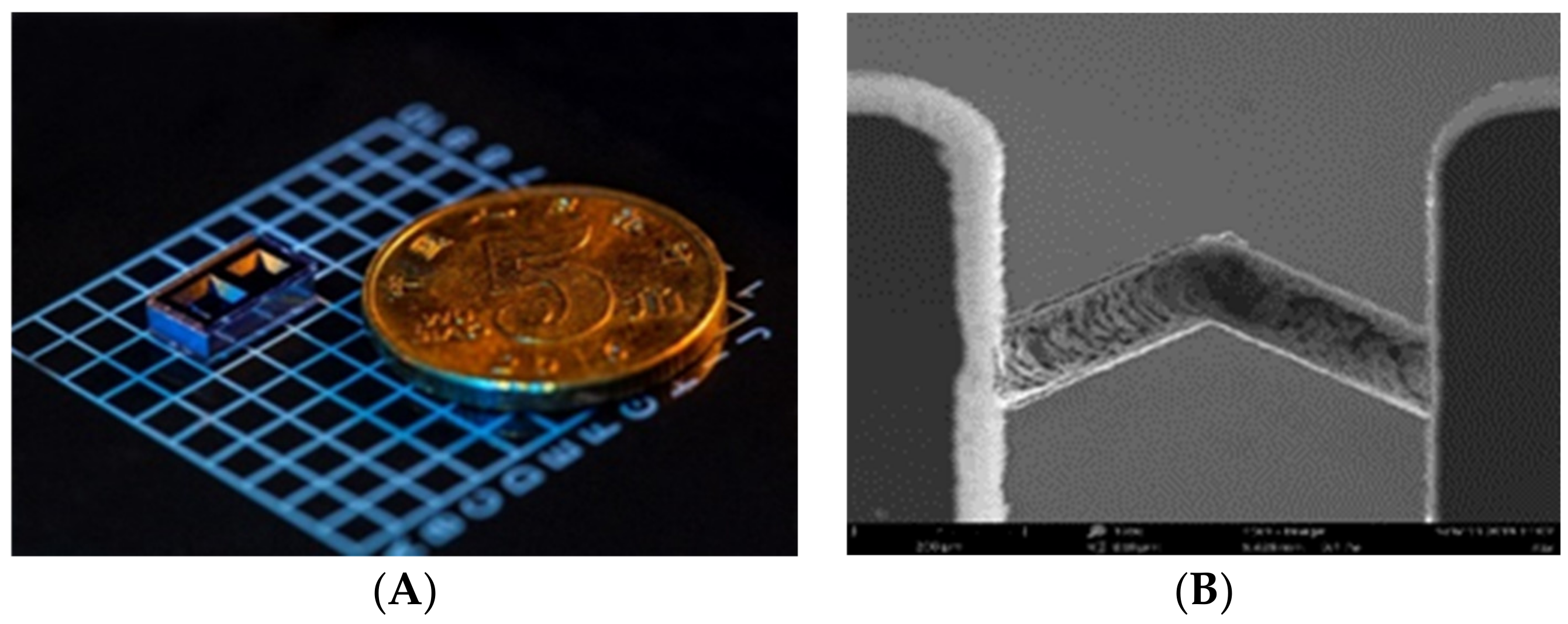
The microfabricated cell, as shown in Figure 1A, has two cavities: one is for containing the rubidium dispenser pill (SAES Getters) and the other one for the optical path. The Rb dispenser, which formed by Rb chromates and an alloy of Zr−Al was stable and nonreactive in an atmosphere environment at room temperature. The solution of single cavities is widely adopted due to its simple geometry and small size. However, in the single cavity, the solid byproducts of the oxidation materials induced by dispenser activation would affect the transmission of light. In the dual-cavity structure, the dispenser is activated by local heating using a 808 nm laser after anodic bonding at a low temperature (<500 °C). Rubidium atom vapor was released by the dispenser and passed through the micro-channel between the two cavities (Figure 1B). The residuals that were left in the dispenser activation cavity did not affect the interaction between incident light and atoms in the other cavity.

Figure 1.
(A) Alkali vapor cell and (B) SEM image of the channel between the two cavities.
The vapor cell was designed as a sandwich structure with one piece of silicon wafer and two pieces of borosilicate glass wafers (BF 33). The silicon wafer with a 4-inch diameter and 1 mm-thick P-type <100> was polished on both sides. The borosilicate glass, 4-inch 1 mm-thick, can be bonded to the silicon wafer by the anodic bonding method because of the similar thermal-expansion coefficients and the low surface roughness and high flatness.
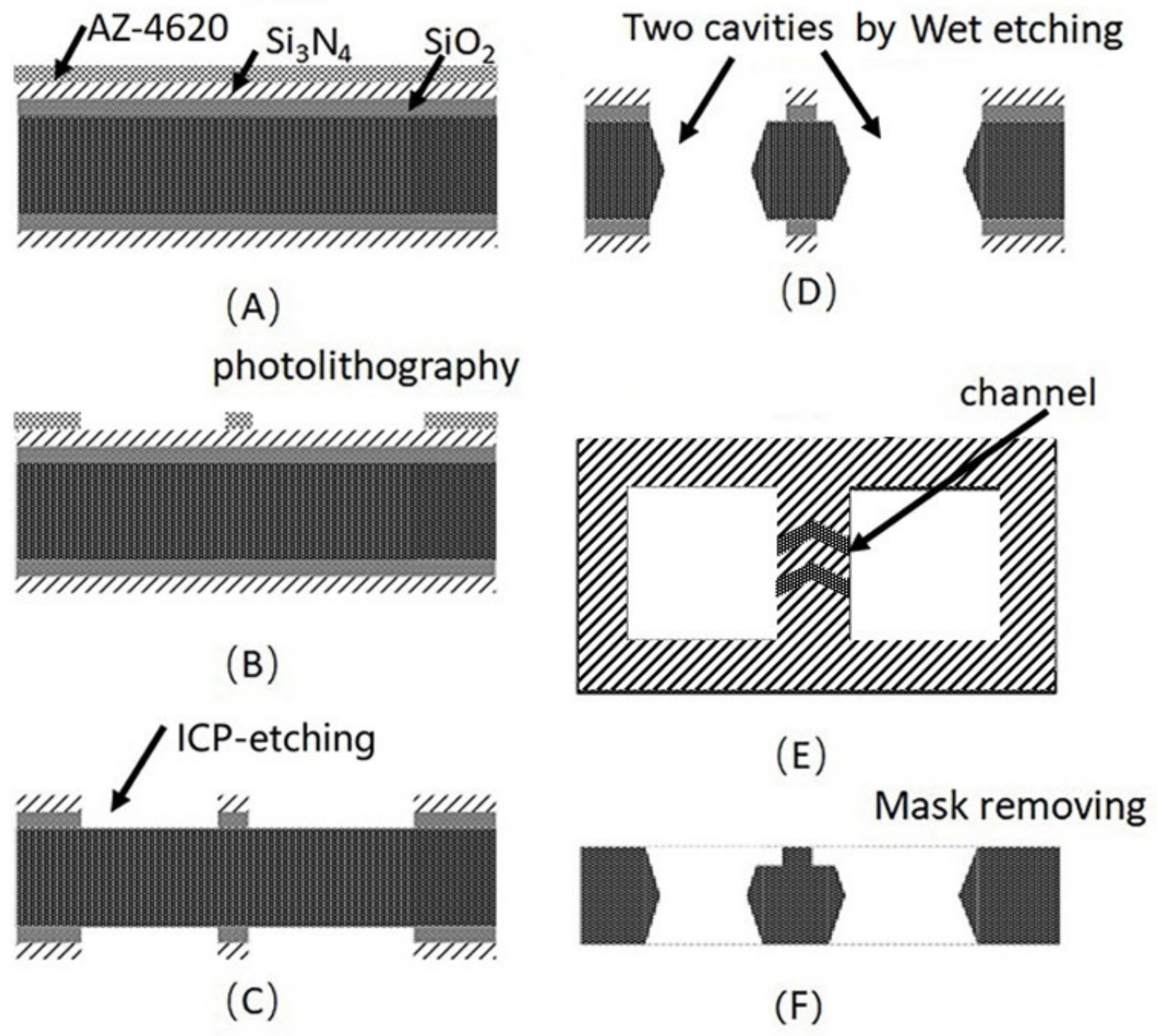
Two through-cavities were etched on a silicon wafer with wet etching, as shown in Figure 2. Firstly, the silicon wafer was rinsed by sufficient acetone, ethanol, and deionized water and was dried in the N2 stream to remove the contaminants on the substrate. Then, the 200 nm SiO2 and 300 nm Si3N4 mask was deposited on the surface of the silicon by plasma enhanced chemical vapor deposition (PECVD) sequentially. After that, positive photoresist (AZ-4620) was spin-coated on the substate of Si3N4 and was patterned by lithography. The exposed SiO2 and Si3N4 was etched by inductively coupled plasma (ICP) etching. Then, the wafer was immerged into the 40% KOH solution in a water bath of about 70 °C to shape the two through-cavities. Finally, the Si3N4 and SiO2 mask was removed by a H3PO4 and HF-based solution sequentially. The two cavities with 2 × 2 mm were used as Rb-dispenser pill (SAES Getters) storage and optical CPT detection, respectively. As shown in Figure 2E, the filtration channels formed by laser etching between two cavities were used for transferring the Rb atoms. Finally, the silicon wafer with two cavities and glasses were cut into 4 × 6 mm chips with an automatic dicing saw (Disco DAD3220).
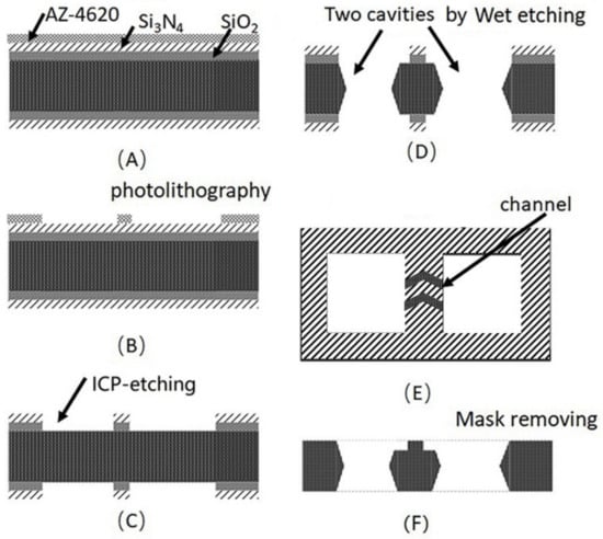
Figure 2.
Fabrication process of the two cavities of the silicon wafer with vapor cell (A) mask deposition, (B) photolithography, (C) ICP-etching for Si3N4 and SiO2. (D) Two cavities by anisotropical etching. (E) The microchannel between two cavities. (F) Si3N4 and SiO2 removing.
The permanent sealing of solid-state materials was mainly realized by bonding technology. Based on electric field-enhancement, anodic bonding, as the key procedure in the fabrication of vapor cell, was used for silicon to glass bonding at a low-temperature (below 500 °C). The permanently bonding interface with a high stability was formed by the voltage between the silicon and glass. Anodic bonding consists mainly of the following three steps: preparation of the surface for bonding, pre-bonding, final formation of bonding [20].
The residues that had a strong impact on the anodic-bonding effect were deposited on the surface of the silicon wafer during the laser etching process. Prior to the anodic-bonding process of 4 × 6 mm silicon and glass chips, the silicon chip with two cavities was polished again by standard polishing process. After that, the cavity-etched silicon and glass chips were cleaned in acetone, ethanol by ultrasonic, and were rinsed in deionized water. After being dried by N2 flow, the chips were baked in an oven at 150 °C for 2 h to evaporate the residual H2O and other gasses.
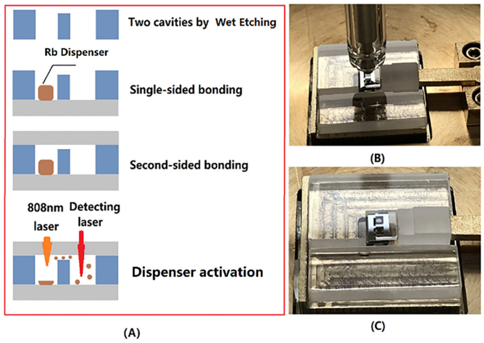
The sealing process of a microfabricated Alkali Vapor Cell, shown in Figure 3A, was performed using the bonding system developed by our team. The procedure mainly followed the following three steps.
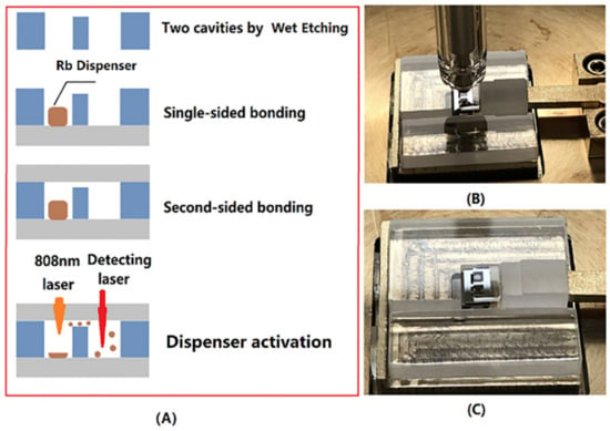
Figure 3.
(A) Sealing process of vapor cell: Single-sided anodic bonding and Rb dispenser storage, Second-sided bonding, dispenser activating and (B) single-chip bonding by the customized bonder with electrode and pressure device, and (C) single-chip bonding with upper glass and lower silicon.
(1) Single-sided bonding: The anodic bonding of the silicon and glass chips were performed at an atmosphere pressure at 350 °C with a bonding voltage 1200 V and 4.5 kN bonding force, by the customized bonder in Figure 3B,C. The bonder was equipped with a sophisticated system for controlling the temperature, voltage, gas pressure, and bonding time. In addition, it had a flexible fixture for 0.3 to 1.5 mm thickness chips within 5 cm for the length or width.
(2) Rb-dispenser packaging by second-sided bonding: The Rb-dispenser was placed into a silicon cavity with a tweezer. Then, the cavities were sealed by second-sided bonding filled with N2 (50, 70, 90 Torr). Based on Paschen’s law, in addition to the relative position of the electrode, the breakdown voltage was decided by the gas species and the pressure of the cavity. The electrode was discharged under N2 (50, 70, and 90 Torr) at 1200 V, although a higher voltage means a better bonding quality, which is crucial to the leak rate and lifetime. For this second-sided anodic bonding, the voltage of the electrode was increased in steps of 100 V from 400 V to 1000 V in an N2 atmosphere. The hermeticity of vapor cell was evaluated by the leakage rate. According to GJB 548B-2005-1014.2, the leakage rate was measured by the following method. For the volume of cavities, about 8 mm3 (<0.05 cm3), the vapor cell was placed into a chamber, followed by pressurizing to 517 kPa of Helium (He) for 2 h. After being taken out from chamber, the vapor cell was degassed by N2 blowing to removing the He attachment. Then, it was put into a mass spectrometer within 1 h to determine the diffused mass of the He. The rejection limit of this leakage test method was 5 × 10⁻⁸ mbar L/s. Finally, the vapor cell passed the test, which means the leak rate was up to 5 × 10⁻⁸ mbar L/s.
(3) Dispenser activation: After the second-sided bonding, the Rb dispenser was sealed hermetically into the cavity, which was filled with N2. According to the previous report, the Rb dispenser could be heated locally by using a diode laser source (808 nm) and released the Rb elemental for CPT signal detection. As Figure 4A shows, the laser beam with 3.5 W was focused on the surface of the Rb dispenser for 2 min to activate the Rb dispenser. The laser beam was transparent to the glass so as to avoid the ablation of other parts of the device. After the activating process, as shown in Figure 4B,D, the dispenser was melted to Rb, Cr2O3, Al2O3, and ZrO2. The droplet shape Rb elemental was deposited on the inner surface of the optical cavity for CPT detection (Figure 4C).
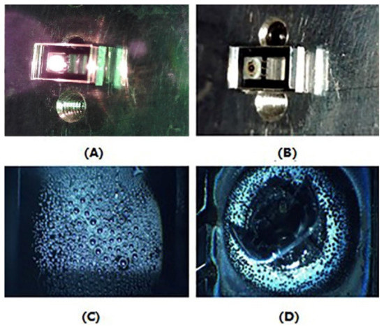
Figure 4.
(A)The activating system with a 808 nm diode laser source; (B,D) the vapor cell after activating by laser; and (C) the Rb elemental on the inner-surface of the optical cavity.
The table-top system (as shown in Figure 5) was constructed for the MEMS cell to detect the coherent population trapping (CPT) resonance, which was used to lock the oscillator in the chip scale atomic clock. The laser was an ECDL laser resonant with the Rb D1 line at 795 nm. It was modulated by the EOM to produce two phase-coherent optical fields with a frequency difference of 6.835 GHz. The 6.835 GHz signal was generated using a commercial microwave synthesizer driven by a 10 MHz quartz crystal local oscillator. The linearly polarized output beam from the laser was converted into circular polarization using a quarter-wave plate. A static magnetic field was applied around the MEMS cell in order to split the Zeeman components and isolate the |F = 1, mF = 0 > → |F = 2, mF = 0 > hyperfine clock transition. The CPT resonance was detected by scanning the 6.835 GHz microwave signal frequency.
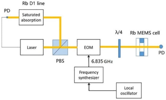
Figure 5.
Schematic of the table-top CPT system with MEMS cell. EOM: electro-optic modulator. PD: photodiode.
3. Results and Discussion
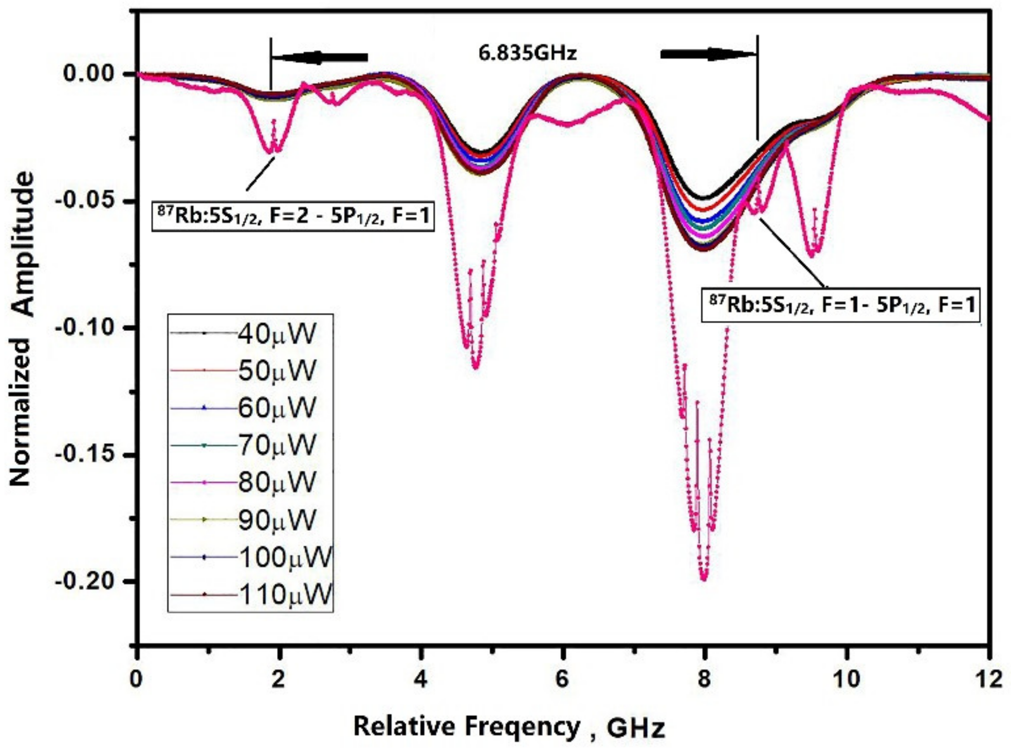
The optical absorption spectroscopy of the microfabricated cell was characterized using a 795 nm ECDL laser resonant with a Rb D1 line to verify the presence the Rb vapor and buffer gas. As Figure 6 shows, a saturated absorption line in a cm-scale pure Rb cell was used as the reference to compare it with the microfabricated cell. The microfabricated cell containing Rb and 70 torr nitrogen was heated to 90 °C to ensure the sufficient density of the atoms, and the absorption spectroscopy of the reference cell was measured at ambient temperature. Although the microcell was heated to 90 °C, the intensity of the absorption peaks was still relatively weak compared to the reference cell due to the only 1 mm optical path in the microfabricated cell. Without buffer gas, two optical absorption peaks (87Rb: Fg = 1 → Fe = 2, Fg = 2 → Fe = 2) of the reference Rb cell were separated by the Rb hyperfine transition frequency and were broadened by the Doppler effect. For the microfabricated cell, the absorption peaks were broadened and shifted by the addition of the buffer gas. The absorption peaks were also broadened by the increasing laser power.
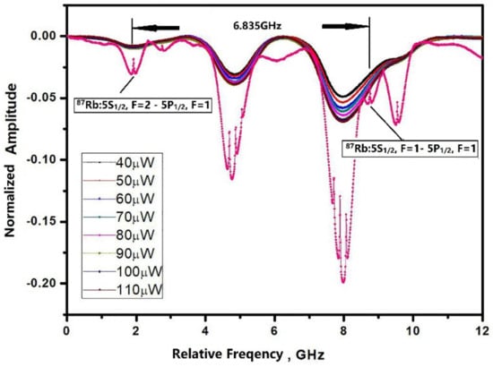
Figure 6.
Optical absorption lines obtained in a cm-scale pure Rb reference cell (Pink dot) compared to a Rb-N2 microfabricated cell heated at 90 °C with laser power from 40 μW to 110 μW.
Figure 7 exhibits the typical result of a CPT resonance in a Rb-N2 MEMS cell heated at 90 °C. The laser beam has a diameter of 1 mm and a power of 120 μW. The 0-0 CPT resonance is well fitted by a Lorentzian function with a linewidth of 28 kHz. The linewidth was about an order of magnitude broader than the typical CPT linewidth based microfabricated cell as the content of N2 was decreased by the absorption of Zr-Al getter in the SAES dispenser [20]. The wall collision decoherence contributed to the abnormal broadening of the CPT linewidth in our results. The contrast of the resonance, which was identified as the ratio between the height and the DC background, was measured to be 1.1%. It did not clamp the expected short-term frequency stability (1 × 10⁻¹⁰) of the chip scale atomic clock [21].
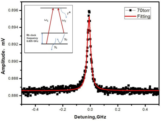
Figure 7.
Typical CPT resonance obtained in a Rb-N2 cell (inset: simplified schematic of three-level system involved in Rb cells CPT resonances, Γ*: linewidth of the optical resonance). The red line is a Lorentzian fit to the experimental data (black dot).
A CPT resonance line shape can be fitted by Lorentzian, and its full width at half maximum FWHM is given by the following [22]:
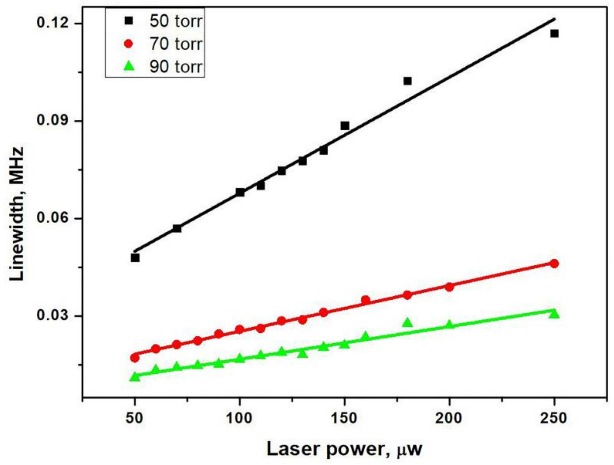
where γ2 is the hyperfine coherence relaxation rate, Γ* is the linewidth of the optical resonance, and ωR is the optical Rabi oscillation frequency related to the laser intensity I (ωR2 ∝ I2 laser power). So, as shown in the Figure 8, the CPT linewidth increases linearly with the laser power. The slope of linear fitting in Figure 8 decreases as the buffer gas pressure increases due to the pressure broadening of the optical resonance (Γ* = Γ + kP). This means that in our anodic bonding system, the buffer gases of different pressure were filled in the microfabricated cells. The CPT linewidth was dominated by collisions of the atoms with the cell walls, and the N2 was utilized to prevent the diffusion and decoherence of atoms. Therefore, under the same optical power, the linewidth of the CPT signal was gradually narrowed as the buffer gas pressure increased (50–90 torr). This is shown in Figure 8. The linewidth is related to the different relaxation rates, as shown in the following Equation (2) [23]:
where γRb-wall represents the effect of alkali-wall collisions, γRb-BG stands for alkali-buffer gas collisions, and γse represents the contribution to the ground state coherence of the Rb–Rb spin-exchange collision. L and R are the length and the radius of the cell, respectively, and D0 is the diffusion constant of Rb atoms in abuffer gas at pressure P0 = 101.3 kPa. P is the pressure of the buffer gas. N0 is the Loschimdt constant, is the relative velocity of Rb atoms with respect to the buffer gas atoms, and is the collisional cross-section between Rb and the buffer gas atoms. is the Rb spin-exchange cross-section. n the number density of Rb. The filled buffer gas is utilized to suppress the decoherence collisions of the atoms to narrow the FWHM of the CPT signal. This narrowing effect of the CPT signal can be explained by the equation above, but it is not linearly dependent on the pressure. This also explains why the narrowing effect of the buffer gas gradually weakened with the increasing pressure (50–70–90 Torr). Furthermore, the linewidth was broadened by the increasing optical power, which was helpful to increase the signal amplitude. Optical power must be carefully investigated, for it is a trade-off between the linewidth and signal-to-noise ratio.

Figure 8.
CPT linewidth as a function of laser power at different pressure (50–70–90 Torr) and the linear fitting curve.
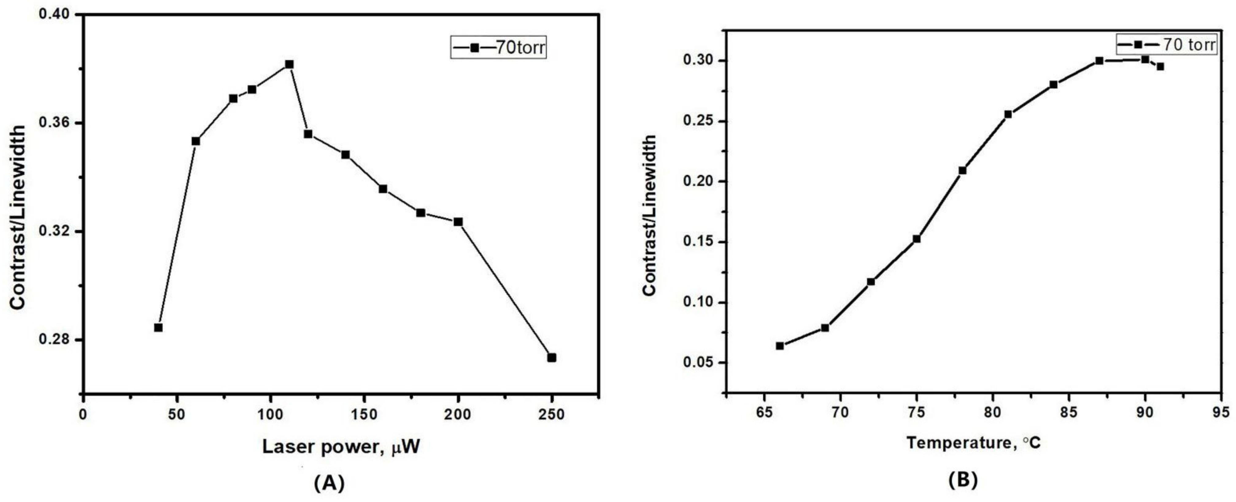
For relevant information in order to optimize the clock short term frequency stability, as shown in the following equation, we investigated the evolution of the ratio between the CPT contrast and the resonance linewidth as a function of the total laser intensity [24].
where represents the shot noise limit, stands for the linewidth of the CPT resonance, ν0 = 6.835 GHz is the microwave frequency, and represents the integration time. Contrast is the ratio between the height of the resonance error signal and the background voltage at the output of photodiode. Pout and νopt are the laser power and light frequency, respectively, and h is the Planck constant. Although the height of the CPT resonance increased with the laser power, the photodetector also received a higher background dc voltage. Therefore, the increase rate of contrast would gradually slow down as the power further increased. The ratio contrast/FWHM finally exhibited a maximum value corresponding to a certain value of laser power, resulting an optimized short-term frequency stability. It is also necessary to investigate the effect the temperature on the ratio contrast/FWHM of the CPT 0-0 resonance. The number of the atoms was restricted by the small volume of the MEMS cell. Increasing the heating temperature would benefit the atomic density and enhance the CPT resonance. However, the amplitude of CPT resonance would drop with the further increase of temperature, which could be explained by the optical density effect. As shown in Figure 9, the ratio contrast/FWHM was found to be maximized for an optical power of 120 μW and a temperature about 90 °C in the MEMS cell with 70 torr buffer gas.
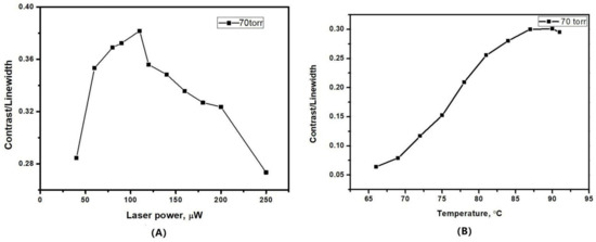
Figure 9.
The ratio contrast/linewidth as a function of (A) laser power and (B) temperature.
4. Conclusions
This paper presents a fast and flexible way of fabricating MEMS cells through improved MEMS technology and anodic bonding. The two hermetic cavities are fabricated by the etching process and glass–silicon–glass single chip anodic bonding in a buffer gas atmosphere. The middle channels are formed by laser micromachining. The detection result of the leak rate was 5 × 10⁻⁸ mbar L/s, which is consistent with the MIL-STD-883E standard (5 × 10⁻⁸ mbar. L/s). A specially designed table-top system for the microfabricated cell has been built to characterize the absorption characteristics and CPT resonance signal. To optimize the short-term frequency stability of the chip scale atomic clock, the MEMS cell was integrated in the table-top CPT systems to investigate the maximized ratio contrast/FWHM. The MEMS cell is deemed suitable for the atomic clock application. Compared with other MEMS vapor cells produced by the research groups, such as NIST and FEMTO-ST, the leak rate and CPT contrast are at the same level. However, the linewidth of CPT is much broader with an inadequate N2 buffer gas. Therefore, the CPT linewidth will be further narrowed by optimizing the N2 pressure in the process of dispenser activation. An atomic clock based on a microfabricated cell will be fabricated in the future. Futhermore, the fatigue behavior and frequency stability will also be studied thoroughly by our group.
Author Contributions
Conceptualization, S.J. and Z.J.; methodology, B.J., X.L. and Z.S.; investigation, S.J.; validation, S.J., Y.P. and Z.J.; formal analysis, Z.J.; writing—original draft preparation, S.J. and Z.J.; writing—review and editing, S.J. and Z.J.; supervision, Z.J. and J.Q.; funding acquisition, Z.J. and Y.P. All authors have read and agreed to the published version of the manuscript.
Funding
This work was supported by the National Natural Science Foundation of China (grant nos. 61805226 and 62075206).
Institutional Review Board Statement
Not applicable.
Informed Consent Statement
Not applicable.
Data Availability Statement
Data and information developed in this research are available.
Conflicts of Interest
The authors declare no conflict of interest.
References
- Godone, A.; Levi, F.; Calosso, C.E.; Micalizio, S. High-performing vapor-cell frequency standards. Riv. Nuovo Cim. 2015, 38, 133–171. [Google Scholar]
- Liew, L.A.; Knappe, S.; Moreland, J.; Robinson, H.; Hollberg, L.; Kitching, J. Microfabricated alkali atom vapor cells. Appl. Phys. Lett. 2004, 84, 2694–2696. [Google Scholar] [CrossRef] [Green Version]
- Knappe, S.; Shah, V.; Schwindt, P.D.D.; Hollberg, L.; Kitching, J. A microfabricated atomic clock. Appl. Phys. Lett. 2004, 85, 1460–1462. [Google Scholar] [CrossRef] [Green Version]
- Gorecki, C.; Hasegawa, M.; Passilly, N.; Chutani, R.K.; Giordano, V. Towards the Realization of the First European MEMS Atomic Clock. In Proceedings of the 2009 IEEE/LEOS International Conference on Optical MEMS and Nanophotonics, Clearwater, FL, USA, 17–20 August 2009. [Google Scholar]
- Alexandrov, E.B. Recent Progress in Optically Pumped Magnetometers. Phys. Scr. 2003, 105, 27–30. [Google Scholar] [CrossRef]
- Griffith, W.C.; Knappe, S.; Kitching, J. Femtotesla atomic magnetometry in a microfabricated vapor cell. Opt. Express 2010, 26, 27167–27172. [Google Scholar] [CrossRef] [PubMed] [Green Version]
- Ji, Y.; Shang, J.; Li, G. Micro-fabricated Shaped Rubidium Vapor Cell for Miniaturized Atomic Magnetometers. IEEE Sens. Lett. 2020, 4, 2500104. [Google Scholar] [CrossRef]
- Kitching, J.; Knappe, S.; Donley, E.A. Atomic Sensors–A Review. IEEE Sens. J. 2011, 9, 1749–1758. [Google Scholar] [CrossRef]
- Kitching, J. Chip-scale atomic devices. Appl. Phys. Rev. 2018, 5, 031302. [Google Scholar] [CrossRef]
- Hummon, M.T.; Kang, S.; Bopp, D.G.; Westly, D.A.; Kitching, J. Photonic chip for laser stabilization to an atomic vapor with 10−11 instability. Optica 2018, 4, 443–449. [Google Scholar] [CrossRef]
- Loh, W.; Hummon, M.T.; Leopardi, H.F. Microresonator Brillouin Laser Stabilization Using a Microfabricated Rubidium Cell. Opt. Express 2016, 24, 14513–14524. [Google Scholar] [CrossRef] [PubMed] [Green Version]
- Hasegawa, M.; Chutani, R.K.; Gorecki, C.; Boudot, R.; Dziuban, P.; Giordano, V.; Clatot, S.; Mauri, L. Microfabrication of cesium vapor cells with buffer gas for MEMS atomic clocks. Sens. Actuators A Phys. 2011, 167, 594–601. [Google Scholar] [CrossRef]
- Miletic, D.; Affolderbach, C.; Mileti, G.; Hasegawa, M.; Gorecki, C. Light shift in CPT based cs miniature atomic clocks. In Proceedings of the International Frequency Control and the European Frequency and Time Forum (FCS) Proceedings, San Francisco, CA, USA, 2–5 May 2011. [Google Scholar]
- Lin, H.; Tian, Y.; Chen, J. Experimental study of the application feasibility of a novel chip-scale atomic clock scheme. Rev. Sci. Instrum. 2019, 90, 053111. [Google Scholar] [CrossRef] [PubMed]
- Ji, Y.; Shang, J.; Zhang, J. Magnetic Gradient Measurement Using Micro-Fabricated Shaped Rubidium Vapor Cell. IEEE Trans. Magn. 2019, 99, 1–5. [Google Scholar] [CrossRef]
- Zhang, L.; Zhang, W.; Zhang, S. Micro-fabrication and hermeticity measurement of alkali-atom vapor cells based on anodic bonding. Chin. Opt. Lett. 2019, 10, 100201. [Google Scholar] [CrossRef]
- Schwindt, P.; Knappe, S.; Shah, V.; Hollberg, L.; Kitching, J.; Liew, L.A. Chip-scale atomic magnetometer. Appl. Phys. Lett. 2004, 85, 6409–6411. [Google Scholar] [CrossRef]
- Knappe, S.A.; Robinson, H.G.; Hollberg, L. Microfabricated saturated absorption laser spectrometer. Opt. Express 2007, 15, 6293–6299. [Google Scholar] [CrossRef] [PubMed]
- Husain, E.; Nema, R.S. Analysis of Paschen Curves for air, N2 and SF6 Using the Townsend Breakdown Equation. IEEE Trans. Electr. Insul. 1982, 17, 350–353. [Google Scholar] [CrossRef]
- Hasegawa, M.; Chutani, R.K.; Gorecki, C. Microfabrication and Thermal Behavior of Miniature Cesium-Vapor Cells For Atomic Clock Operations. In Proceedings of the IEEE International Conference on Micro Electro Mechanical Systems, Cancun, Mexico, 23–27 January 2011. [Google Scholar]
- Post, A.B.; Jau, Y.Y.; Kuzma, N.N. Amplitude-versus frequency-modulated pumping light for coherent population trapping resonances at high buffer-gas pressure. Phys. Rev. A 2005, 72, 2409–2418. [Google Scholar] [CrossRef]
- Vanier, J.; Godone, A.; Levi, F. Coherent population trapping in cesium: Dark lines and coherent microwave emission. Phys. Rev. A 1998, 58, 2345–2358. [Google Scholar] [CrossRef]
- Vanier, J.; Audoin, C. The Quantum Physics of Atomic Frequency Standards; Hilger: Bristol, UK, 1989. [Google Scholar]
- Boudot, R.; Dziuban, P.; Hasegawa, M.; Chutani, R.K.; Galliou, S.; Giordano, V.; Gorecki, C. Coherent population trapping resonances in Cs-Ne vapor microcells for miniature clocks applications. J. Appl. Phys. 2011, 109, 014912. [Google Scholar] [CrossRef]
Publisher’s Note: MDPI stays neutral with regard to jurisdictional claims in published maps and institutional affiliations. |
© 2022 by the authors. Licensee MDPI, Basel, Switzerland. This article is an open access article distributed under the terms and conditions of the Creative Commons Attribution (CC BY) license (https://creativecommons.org/licenses/by/4.0/).

