
Non-Isolated DC-DC Converters in Fuel Cell Applications: Thermal Analysis and Reliability Comparison


Abstract
:1. Introduction
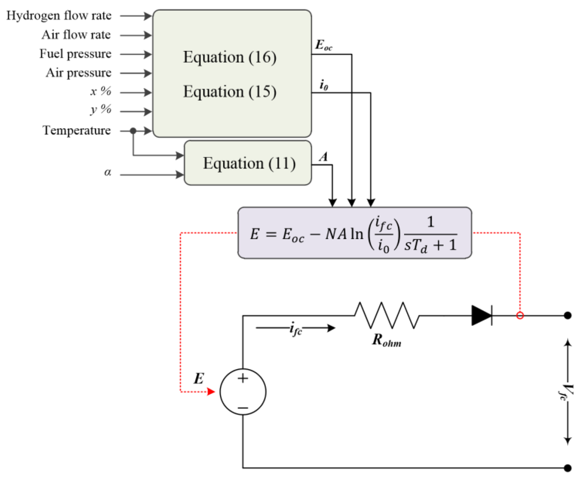
2. Fuel Cell
Fuel Cell Losses
- The gases are ideal.
- The hydrogen and air are fed into the stack.
- The cooling system is embedded so that the temperature of the anode and cathode is stable at the stack temperature.
- A water management system is designed to adjust the humidity inside the cell to an appropriate degree under various conditions.
- Pressure drops across flow channels are ignorable.
- The cell resistance under any operation condition is considered to be constant.
- Considering that in most cases, the fuel cell does not operate in the mass transport region, the mass transport losses or concentration losses are negligible.
- Nominal voltage: 210 V
- Nominal current: 120 A
- Number of cells: 300
- Nominal stack efficiency: 55%
- Operating temperature: 65 °C
- Fuel cell resistance: 0.487 Ω
- Nominal airflow rate: 2100 L/min
3. DC-DC Converters
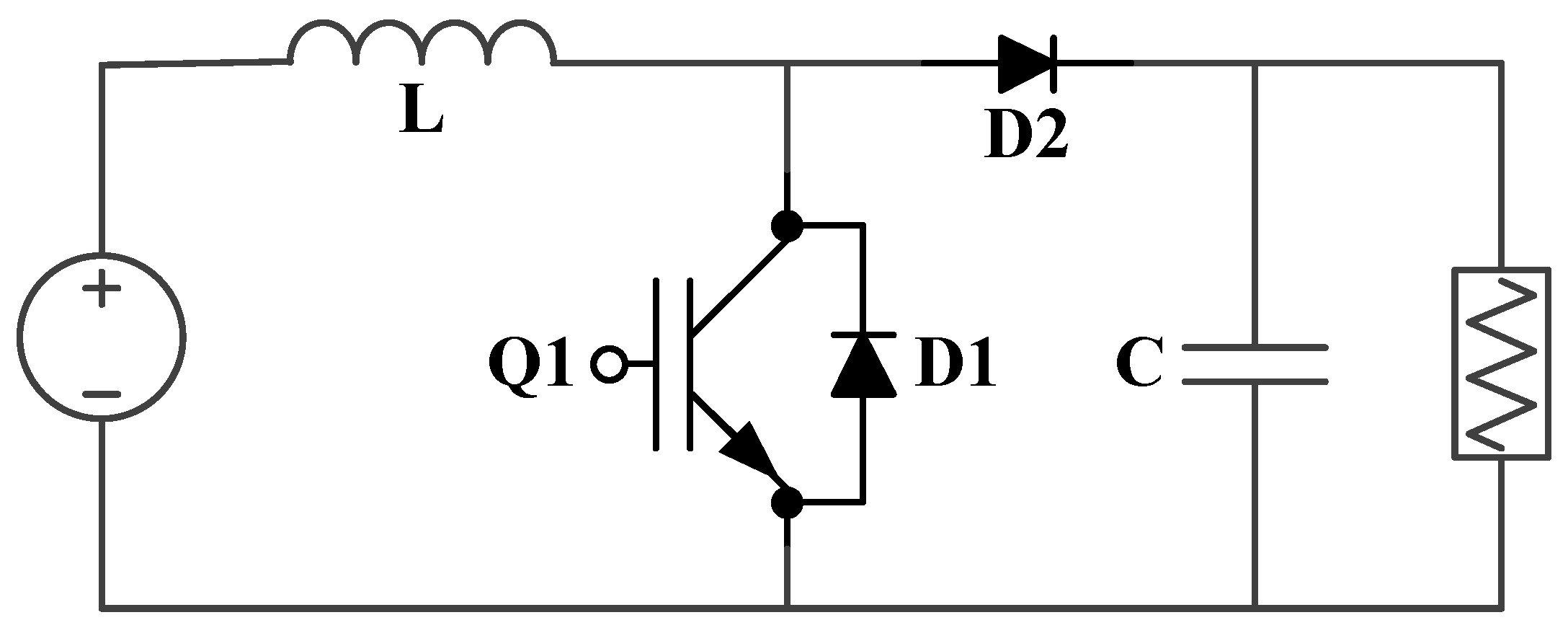
3.1. Boost Converter
- Continuous input current
- Has the smallest possible number of components
- Simple drive circuit due to the grounded switch used in this topology
- Requiring a large capacitor size
- Poor efficiency for very large duty cycles
- Non-isolated input from the output
- High switching noise
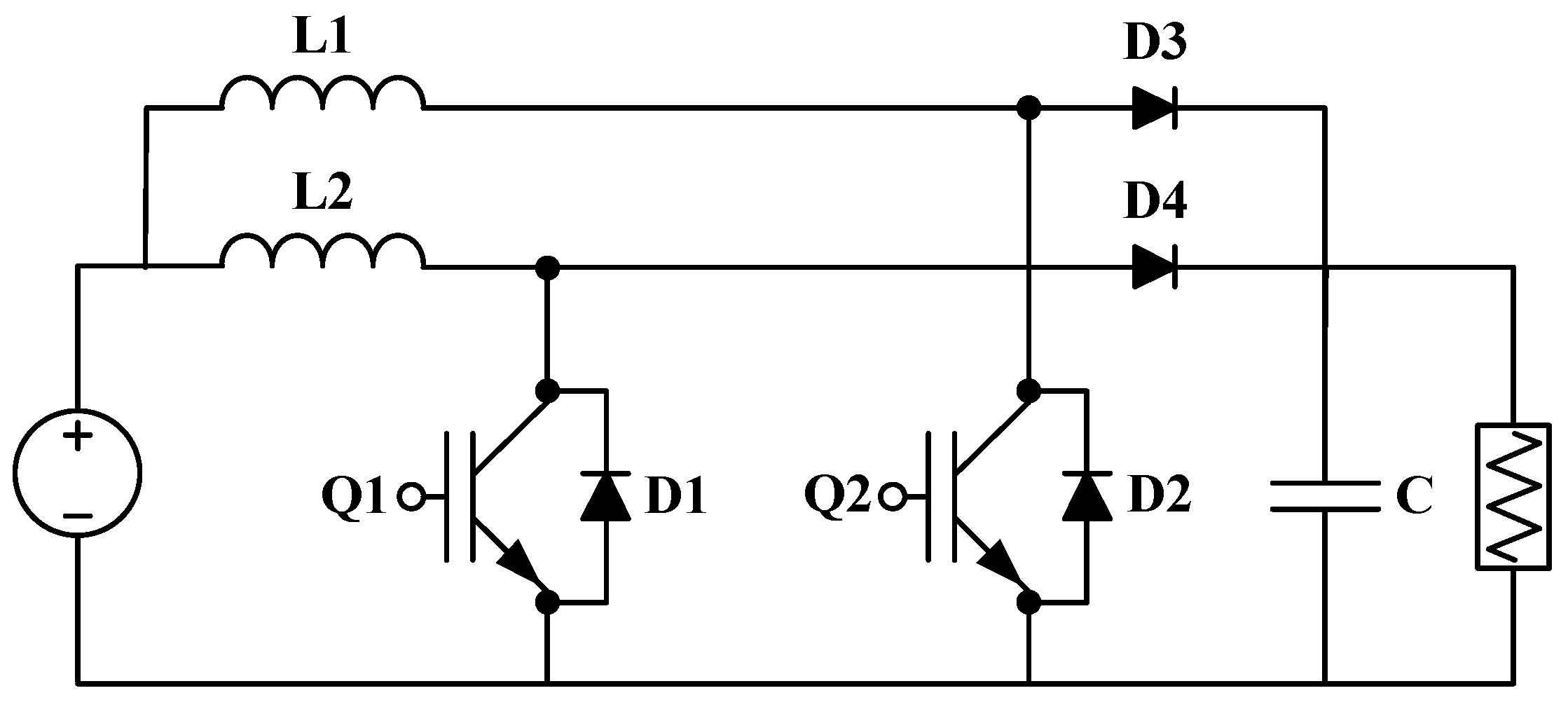
3.2. Interleaved Boost Converter
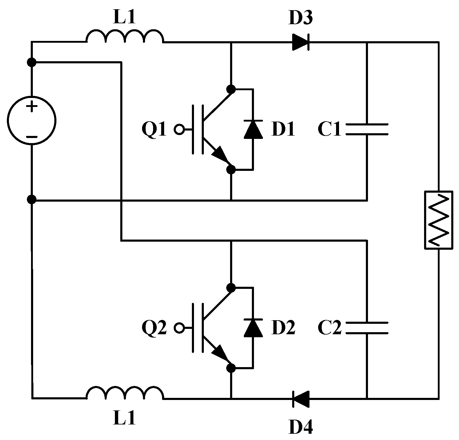
3.3. Floating Interleaved Boost Converter
- Higher efficiency
- Higher voltage ratio for the converter
- Higher input and output frequency—fewer losses
- Improved reliability due to the parallel structure
- Reduced size of the parasitic elements, weight, and volume
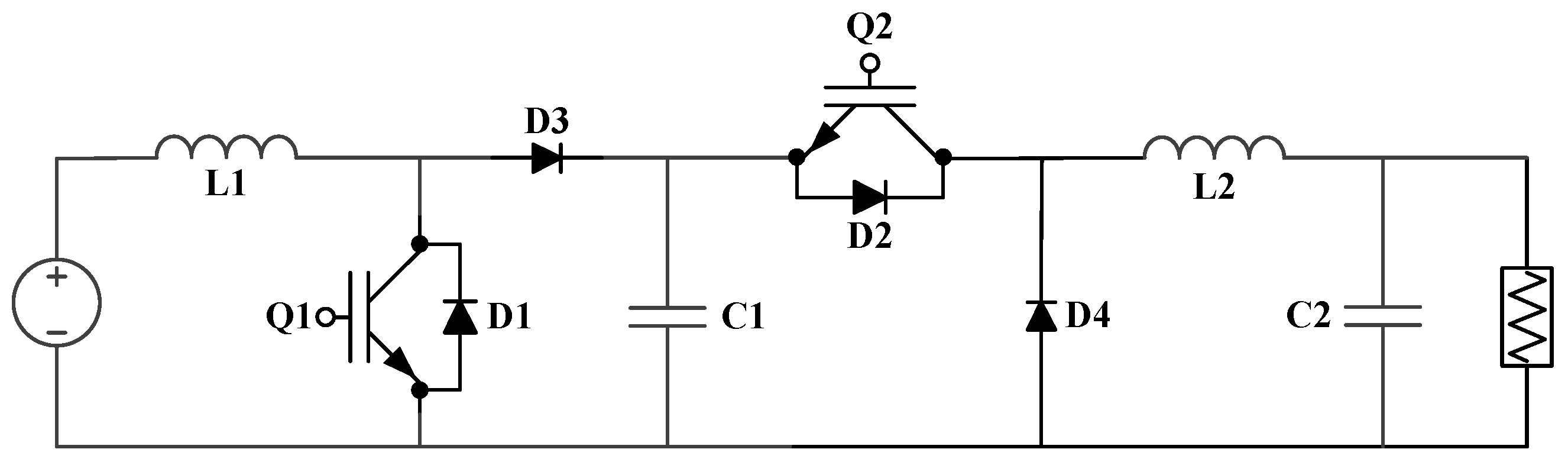
3.4. Multi-Switch Boost Converter
3.5. Cuk Converter
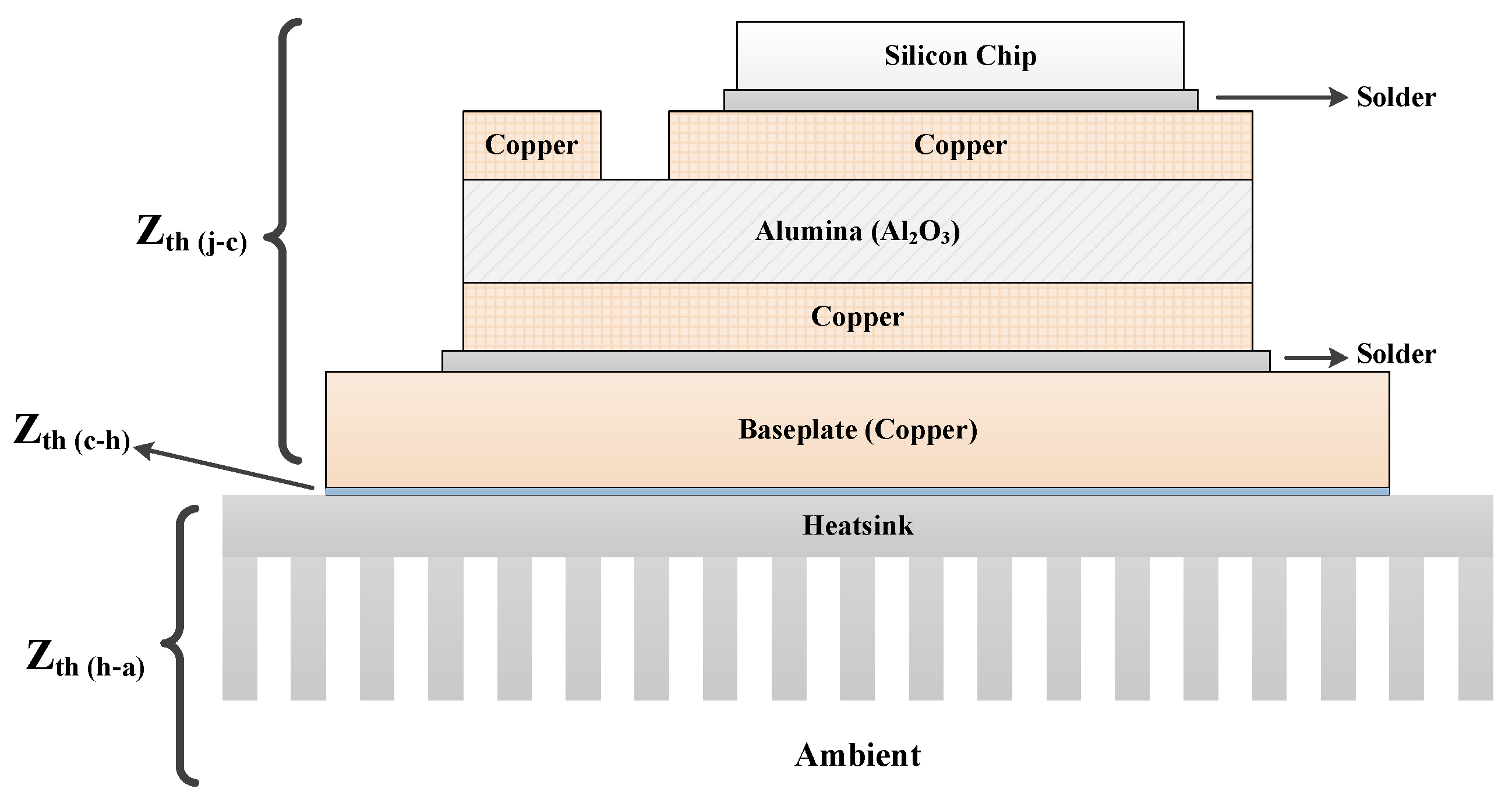
4. Thermal Model of Power Semiconductors
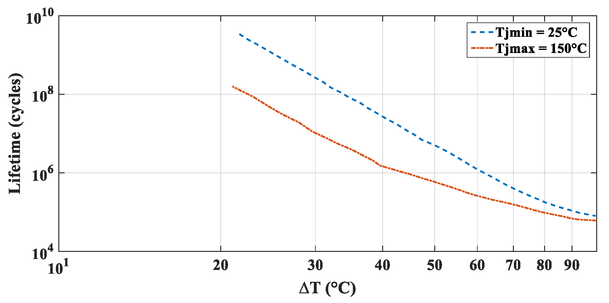
5. Reliability Evaluation
6. Results and Discussion
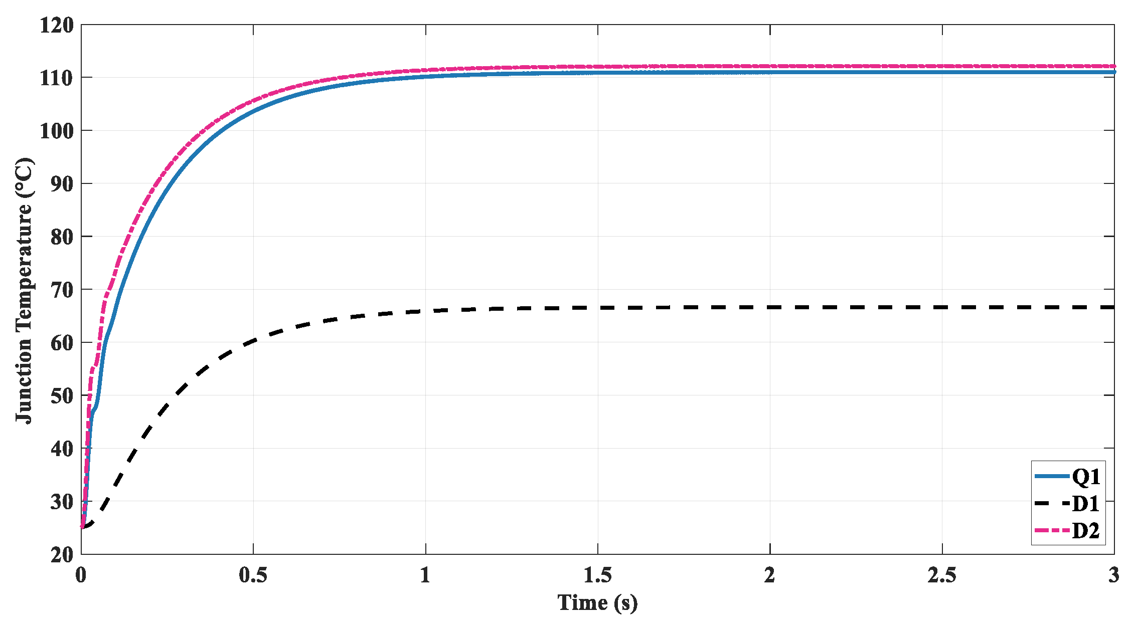
6.1. Conventional Boost Converter
6.2. Interleaved Boost Converter
6.3. Floating Interleaved Boost Converter
6.4. Multi-Switch Boost Converter
6.5. Cuk Converter
6.6. Reliability Assessment
- Conventional Boost: D2 and Q1
- Interleaved Boost: D3 (or D4) and Q1 (or Q2)
- Floating Interleaved Boost: D3 (or D4) and Q1 (or Q2)
- Multi-switch Boost: D3 and Q2
- Cuk: D2 and Q1
- Calculate the normalized decision matrix based on the normalized values as follows:
- Calculate the weighted normalized decision matrix by multiplying the selected weights by the normalized values as follows:
- 3.
- Determine the positive and negative ideal solutions:where,
- 4.
- Calculate the distance of each alternative from the ideal solution by using the Euclidean distance formula as follows:
- 5.
- Calculate the relative closeness for each alternative as the performance score by dividing its positive ideal solution by the summation of its ideal solutions:
7. Conclusions
Author Contributions
Funding
Institutional Review Board Statement
Informed Consent Statement
Data Availability Statement
Conflicts of Interest
References
- Rajabloo, T.; De Ceuninck, W.; Van Wortswinkel, L.; Rezakazemi, M.; Aminabhavi, T. Environmental management of industrial decarbonization with focus on chemical sectors: A review. J. Environ. Manag. 2022, 302, 114055. [Google Scholar] [CrossRef]
- Andujar, J.M.; Segura, F.; Vasallo, M.J. A suitable model plant for control of the set fuel cell-DC/DC converter. Renew. Energy 2008, 33, 813–826. [Google Scholar] [CrossRef]
- Barbir, F.; Molter, T.; Dalton, L. Efficiency and weight trade-off analysis of regenerative fuel cells as energy storage for aerospace applications. Int. J. Hydrogen Energy 2005, 30, 351–357. [Google Scholar] [CrossRef]
- Wilberforce, T.; Alaswad, A.; Palumbo, A.; Dassisti, M.; Olabi, A.G. Advances in stationary and portable fuel cell applications. Int. J. Hydrogen Energy 2016, 41, 16509–16522. [Google Scholar] [CrossRef] [Green Version]
- Fadzillah, D.M.; Kamarudin, S.K.; Zainoodin, M.A.; Masdar, M.S. Critical challenges in the system development of direct alcohol fuel cells as portable power supplies: An overview. Int. J. Hydrogen Energy 2019, 172, 207–219. [Google Scholar] [CrossRef]
- Serincan, M.F. Validation of hybridization methodologies of fuel cell backup power systems in real-world telecom applications. Int. J. Hydrogen Energy 2016, 42, 19129–19140. [Google Scholar] [CrossRef]
- Kuo, J.K.; Wang, C.F. An integrated simulation model for PEM fuel cell power systems with a buck DC-DC converter. Int. J. Hydrogen Energy 2011, 36, 11846–11855. [Google Scholar] [CrossRef]
- Fabbri, E.; Bi, L.; Pergolesi, D.; Traversa, E. Towards the next generation of solid oxide fuel cells operating below 600 °C with chemically stable proton-conducting electrolytes. Adv. Mater. 2012, 24, 195–208. [Google Scholar] [CrossRef]
- Slah, F.; Mansour, A.; Hajer, M.; Faouzi, B. Analysis, modeling and implementation of an interleaved boost DC-DC converter for fuel cell used in electric vehicle. Int. J. Hydrogen Energy 2017, 42, 28852–28864. [Google Scholar] [CrossRef]
- Thounthong, P.; Raël, S.; Davat, B. Test bench of a PEM fuel cell with low voltage static converter. J. Power Sources 2006, 153, 145–150. [Google Scholar] [CrossRef]
- Palma, L.; Todorovic, M.H.; Enjeti, P. A high gain transformerless DC-DC converter for fuel cell applications. In Proceedings of the Annual IEEE Conference on Power Electronics Specialists (PESC), Dresden, Germany, 16 June 2005; pp. 2514–2520. [Google Scholar]
- Gerard, M.; Poirot-Crouzevier, J.P.; Hissel, D.; Pera, M. Ripple current effects on PEMFC aging test by experimental and modeling. J. Fuel Cell Sci. Technol. 2011, 8, 021004. [Google Scholar] [CrossRef]
- Valdez-resendiz, J.E.; Sanchez, V.M.; Rosas-caro, J.C.; Mayomaldonado, J.C.; Sierra, J.M.; Barbosa, R. Continuous input-current buck-boost DC-DC converter for PEM fuel cell applications. Int. J. Hydrogen Energy 2017, 42, 30389–30399. [Google Scholar] [CrossRef]
- Pathapati, P.R.; Xue, X.; Tang, J. A new dynamic model for predicting transient phenomena in a PEM fuel cell system. Renew. Energy 2005, 30, 1–22. [Google Scholar] [CrossRef]
- Moreira, M.V.; da Silva, G.E. A practical model for evaluating the performance of proton exchange membrane fuel cells. Renew. Energy 2009, 34, 1734–1741. [Google Scholar] [CrossRef]
- Al-Baghdadi, M.S. Modelling of proton exchange membrane fuel cell performance based on semiempirical equations. Renew. Energy 2005, 30, 1587–1599. [Google Scholar] [CrossRef]
- Arasaratnam, I. A simplified design, control and power management of fuel cell vehicles. SAE Tech. Pap. 2014. [Google Scholar] [CrossRef] [Green Version]
- Han, J.; Charpentier, J.F.; Tang, T. An energy management system of a fuel cell/battery hybrid boat. Energies 2014, 7, 2799–2820. [Google Scholar] [CrossRef] [Green Version]
- Motapon, S.N. A Generic Fuel Cell Model and Experimental Validation. Master’s Thesis, École de Technologie Supérieure (ÉTS), Montreal, QC, Canada, 2008. [Google Scholar]
- Bizon, N.; Mazare, A.G.; Ionescu, L.M.; Enescu, F.M. Optimization of the proton exchange membrane fuel cell hybrid power system for residential buildings. Energy Convers. Manag. 2018, 163, 22–37. [Google Scholar] [CrossRef]
- Christou, A.G. Hydrogen Fuel Cell Power System Performance of Plug Power Gen Core 5B48 Unit. Master’s Thesis, University of Strathclyde, Glasgow, Scotland, 2010. [Google Scholar]
- O’Hayre, R.; Cha, S.W.; Colella, W.; Brinz, F.B. Fuel Cell Fundamentals; Wiley: New York, NY, USA, 2006. [Google Scholar]
- Abd El Monem, A.A.; Azmy, A.M.; Mahmoud, S.A. Effect of process parameters on the dynamic behavior of polymer electrolyte membrane fuel cells for electric vehicle applications. Ain Shams Eng. J. 2014, 5, 75–84. [Google Scholar] [CrossRef] [Green Version]
- Kunusch, C.; Puleston, P.; Mayosky, M. Sliding-Mode Control of PEM Fuel Cells; Springer: London, UK, 2012. [Google Scholar]
- Jianfeng, H.; Liangfei, X.; Xinfan, L.; Languang, L.; Minggao, O. Modeling and experimental study of PEM fuel cell transient response for automotive applications. Tsinghua Sci. Technol. 2009, 14, 639–645. [Google Scholar]
- Hwang, J.J.; Kuo, J.K.; Wu, W.; Chang, W.R.; Lin, C.H.; Wang, S.E. Life cycle performance assessment of fuel cell/battery electric vehicles. Int. J. Hydrogen Energy 2013, 38, 3433–3446. [Google Scholar] [CrossRef]
- Motapon, S.N.; Tremblay, O.; Dessaint, L.A. Development of a generic fuel cell model: Application to a fuel cell vehicle simulation. Int. J. Power Electron. 2012, 4, 505–522. [Google Scholar] [CrossRef]
- Bicer, Y.; Dincer, I.; Aydin, M. Maximizing performance of fuel cell using artificial neural network approach for smart grid applications. Energy 2016, 116, 1205–1217. [Google Scholar] [CrossRef]
- Haibo, Q.; Yicheng, Z.; Yongtao, Y.; Li, W. Analysis of buck–boost converters for fuel cell electric vehicles. In Proceedings of the IEEE International Conference on Vehicular Electronics and Safety (ICVES), Shanghai, China, 13–15 December 2006; pp. 109–113. [Google Scholar]
- Prudente, M.; Pfitscher, L.L.; Emmendoerfer, G.; Romaneli, E.F.; Gules, R. Voltage multiplier cells applied to non-isolated DC-DC converters. IEEE Trans. Power Electron. 2008, 23, 871–887. [Google Scholar] [CrossRef]
- Hu, X.; Gong, C. A high voltage gain dc–dc converter integrating coupled-inductor and diode–capacitor techniques. IEEE Trans. Power Electron. 2014, 29, 789–800. [Google Scholar]
- Schimpf, F.; Norum, L.E. Grid connected converters for photovoltaic, state of the art, ideas for improvement of transformerless inverters. In Proceedings of the Nordic Workshop on Power and Industrial Electronics (NORPIE), Espoo, Finland, 9–11 June 2008. [Google Scholar]
- Palma, L.; Todorovic, M.H.; Enjeti, P. Design considerations for a fuel cell powered dc–dc converter for portable applications. In Proceedings of the Annual IEEE Conference on Applied Power Electronics Conference and Exposition (APEC), Dallas, TX, USA, 19–23 March 2006; pp. 19–23. [Google Scholar]
- Ali, M.S.; Kamarudin, S.K.; Masdar, M.S.; Mohamed, A. An overview of power electronics applications in fuel cell systems: DC and AC converters. Sci. World J. 2014, 2014, 103709. [Google Scholar] [CrossRef]
- Meng, H. Synchronous or Nonsynchronous Topology? Boost System Performance with the Right DC-DC Converter. Maxim Integrated® Application Note. Available online: http://www.maximintegrated.com/en/design/technical-documents/app-notes/6/6129.html (accessed on 14 May 2022).
- Romadhon, M.I.; Andromeda, T.; Facta, M.; Warsito, A. A comparison of synchronous and nonsynchronous boost converter. IOP Conf. Ser. Mater. Sci. Eng. 2017, 190, 012021. [Google Scholar] [CrossRef] [Green Version]
- Martinez, W.; Imaoka, J.; Itoh, Y.; Yamamoto, M.; Umetani, K. Analysis of coupled-inductor configuration for an interleaved high step-up converter. In Proceedings of the International Conference on Power Electronics (ICPE), Seoul, Korea, 1–5 June 2015; pp. 2591–2598. [Google Scholar]
- Kosai, H.; McNeal, S.; Page, A.; Jordan, B.; Scofield, J.; Ray, B. Characterizing the effects of inductor coupling on the performance of an interleaved boost converter. In Proceedings of the Annual Passive Components Conference (CARTS), Jacksonville, FL, USA, 30 March 2009; pp. 237–251. [Google Scholar]
- Rahavi, J.S.A.; Kanagapriya, T.; Seyezhai, R. Design and analysis of interleaved boost converter for renewable energy source. In Proceedings of the International Conference on Computing, Electronics and Electrical Technologies (ICCEET), Nagercoil, India, 21–22 March 2012; pp. 447–451. [Google Scholar]
- Seyezhai, R.; Mathur, B.L. Design and implementation of interleaved boost converter for fuel cell systems. Int. J. Hydrogen Energy 2012, 37, 3897–3903. [Google Scholar] [CrossRef]
- Kabalo, M.; Paire, D.; Blunier, B.; Bouquain, D.; Simoes, M.G.; Miraoui, A. Experimental evaluation of four-phase floating interleaved boost converter design and control for fuel cell applications. IET Power Electron. 2013, 6, 215–226. [Google Scholar] [CrossRef] [Green Version]
- Kabalo, M.; Blunier, B.; Bouquain, D.; Miraoui, A. State-of-the-art of DC/DC converters for fuel cell vehicles. In Proceedings of the IEEE Conference on Vehicle Power and Propulsion (VPPC), Lille, France, 1–3 September 2010; pp. 1–6. [Google Scholar]
- Garrigos, A.; Sobrino-Manzanares, F. Interleaved multi-phase and multi-switch boost converter for fuel cell applications. Int. J. Hydrogen Energy 2015, 40, 8419–8432. [Google Scholar] [CrossRef]
- Xu, W.; Cheng, K.W.; Chan, K.W. Application of Cuk converter together with battery technologies on the low voltage DC supply for electric vehicles. In Proceedings of the International Conference on Power Electronics Systems and Applications (ICPESA), Hong Kong, China, 15–17 December 2015; pp. 1–5. [Google Scholar]
- Huang, W.; Yen, K.; Roig, G.; Lee, E. Voltage divided noninverting Cuk converter with large conversion ratios. In Proceedings of the IEEE Southeastcon, Williamsburg, VA, USA, 7–10 April 1991; pp. 1005–1007. [Google Scholar]
- Salah, W.; Taib, S.; Al-Mofleh, A. Development of multistage converter for outdoor thermal electric cooling (TEC) applications. Jordan J. Mech. Ind. Eng. 2010, 4, 15–20. [Google Scholar]
- Alavi, O.; Viki, A.H.; Bina, M.T.; Akbari, M. Reliability assessment of a stand-alone wind-hydrogen energy conversion system based on thermal analysis. Int. J. Hydrogen Energy 2017, 42, 14968–14979. [Google Scholar] [CrossRef]
- Ciappa, M.; Carbognani, F. Lifetime prediction and design of reliability tests for high power devices in automotive applications. IEEE Trans. Device Mater. Reliab. 2003, 3, 191–196. [Google Scholar] [CrossRef]
- Ma, K.; Liserre, M.; Blaabjerg, F.; Kerekes, T. Thermal loading and lifetime estimation for power device considering mission profiles in wind power converter. IEEE Trans. Power Electron. 2015, 30, 590–602. [Google Scholar] [CrossRef]
- Strickland, P.R. The thermal equivalent circuit of a transistor. IBM J. Res. Dev. 1959, 3, 35–45. [Google Scholar] [CrossRef]
- Alavi, O.; Abdollah, M.; Viki, A.H. Assessment of thermal network models for estimating IGBT junction temperature of a buck converter. In Proceedings of the Power Electronic and Drive Systems and Technologies Conference (PEDSTC), Mashhad, Iran, 14–16 February 2017; pp. 102–107. [Google Scholar]
- Hnatek, E.R. Practical Reliability of Electronic Equipment and Products; CRC Press: New York, NY, USA, 2002. [Google Scholar]
- Wintrich, A.; Nicolai, U.; Tursky, W.; Reimann, T. Application Manual Power Semiconductors; Semikron International GmbH: Nuremberg, Germany, 2011. [Google Scholar]
- Chung, H.S.H.; Wang, H.; Blaabjerg, F.; Pecht, M. Reliability of Power Electronic Converter Systems; Institution of Engineering and Technology: London, UK, 2015. [Google Scholar]
- Cui, H. Accelerated temperature cycle test and Coffin–Manson model for electronic packaging. In Proceedings of the Annual Symposium on Reliability and Maintainability (RAMS), Alexandria, VA, USA, 24–27 January 2005; pp. 556–560. [Google Scholar]
- Busca, C.; Teodorescu, R.; Blaabjerg, F.; Munk-Nielsen, S.; Helle, L.; Abeyasekera, T.; Rodriguez, P. An overview of the reliability prediction related aspects of high power IGBTs in wind power applications. Microelectron. Reliab. 2011, 51, 1903–1907. [Google Scholar] [CrossRef] [Green Version]
- Wang, B.; Cai, J.; Du, X.; Zhou, L. Review of power semiconductor device reliability for power converters. CPSS Trans. Power Electron. Appl. 2017, 2, 101–117. [Google Scholar] [CrossRef]
- Sadigh, A.K.; Dargahi, V.; Abarzadeh, M.; Dargahi, S. Reduced DC voltage source flying capacitor multicell multilevel inverter: Analysis and implementation. IET Power Electron. 2014, 7, 439–450. [Google Scholar] [CrossRef]
- Hwang, C.L.; Yoon, K.P. Multiple Attribute Decision Making: Methods and Applications; Springer: New York, NY, USA, 1981. [Google Scholar]
- Behzadian, M.; Khanmohammadi Otaghsara, S.; Yazdani, M.; Ignatius, J. A state-of the-art survey of TOPSIS applications. Expert Syst. Appl. 2012, 39, 13051–13069. [Google Scholar] [CrossRef]
- Opricovic, S.; Tzeng, G.H. Compromise solution by MCDM methods: A comparative analysis of VIKOR and TOPSIS. Eur. J. Oper. Res. 2004, 156, 445–455. [Google Scholar] [CrossRef]


| Converters | Tjmax (°C) | Tjmin (°C) | Tjm (°C) | ∆Tj (°C) | Nf (No. Cycles) |
|---|---|---|---|---|---|
| Conventional Boost | 113.60 | 34.47 | 74.04 | 79.13 | 174,568 |
| Interleaved Boost | 65.41 | 29.44 | 47.43 | 35.97 | 6,350,411 |
| Floating Interleaved Boost | 58.72 | 29.20 | 43.96 | 29.52 | 15,325,855 |
| Multi-switch Boost | 65.87 | 28.89 | 47.38 | 36.98 | 5,635,353 |
| Cuk | 99.87 | 31.52 | 65.70 | 68.35 | 347,316 |
| Converters | Nf(No. Cycles) | Tjmax (Q) (°C) | Tjmax (D) (°C) | No. Components | Cost |
|---|---|---|---|---|---|
| Conventional Boost | 174,568 | 111.00 | 112.10 | 5 | Very Low |
| Interleaved Boost | 6,350,411 | 69.94 | 91.66 | 9 | High |
| Floating Interleaved Boost | 15,325,855 | 62.25 | 56.65 | 10 | High |
| Multi-switch Boost | 5,635,353 | 71.12 | 97.76 | 7 | Average |
| Cuk | 347,316 | 106.50 | 94.94 | 10 | High |
| Converters | Performance Score (P) | Rank |
|---|---|---|
| Conventional Boost | 0.3306 | 4 |
| Interleaved Boost | 0.3553 | 3 |
| Floating Interleaved Boost | 0.6694 | 1 |
| Multi-switch Boost | 0.3679 | 2 |
| Cuk | 0.1092 | 5 |
| Converters | Performance Score (P) | Rank |
|---|---|---|
| Conventional Boost | 0.2631 | 4 |
| Interleaved Boost | 0.3782 | 2 |
| Floating Interleaved Boost | 0.7369 | 1 |
| Multi-switch Boost | 0.3690 | 3 |
| Cuk | 0.0579 | 5 |
Publisher’s Note: MDPI stays neutral with regard to jurisdictional claims in published maps and institutional affiliations. |
© 2022 by the authors. Licensee MDPI, Basel, Switzerland. This article is an open access article distributed under the terms and conditions of the Creative Commons Attribution (CC BY) license (https://creativecommons.org/licenses/by/4.0/).
Share and Cite
Alavi, O.; Rajabloo, T.; De Ceuninck, W.; Daenen, M. Non-Isolated DC-DC Converters in Fuel Cell Applications: Thermal Analysis and Reliability Comparison. Appl. Sci. 2022, 12, 5026. https://doi.org/10.3390/app12105026
Alavi O, Rajabloo T, De Ceuninck W, Daenen M. Non-Isolated DC-DC Converters in Fuel Cell Applications: Thermal Analysis and Reliability Comparison. Applied Sciences. 2022; 12(10):5026. https://doi.org/10.3390/app12105026
Chicago/Turabian StyleAlavi, Omid, Talieh Rajabloo, Ward De Ceuninck, and Michaël Daenen. 2022. "Non-Isolated DC-DC Converters in Fuel Cell Applications: Thermal Analysis and Reliability Comparison" Applied Sciences 12, no. 10: 5026. https://doi.org/10.3390/app12105026
APA StyleAlavi, O., Rajabloo, T., De Ceuninck, W., & Daenen, M. (2022). Non-Isolated DC-DC Converters in Fuel Cell Applications: Thermal Analysis and Reliability Comparison. Applied Sciences, 12(10), 5026. https://doi.org/10.3390/app12105026