Article

Design of a Laser Driver and Its Application in Gas Sensing

1
Key Laboratory of Intelligent Manufacturing Technology, College of Engineering, Inner Mongolia Minzu University, Tongliao 028000, China
2
College of Information Science and Technology, Dalian Maritime University, Dalian 116026, China
3
State Key Laboratory on Integrated Optoelectronics, College of Electronic Science and Engineering, Jilin University, Changchun 130012, China
4
Zhongke Wind Power Co., Ltd., Tongliao 028000, China
*
Author to whom correspondence should be addressed.
Appl. Sci. 2022, 12(12), 5883; https://doi.org/10.3390/app12125883
Submission received: 9 May 2022 / Revised: 2 June 2022 / Accepted: 6 June 2022 / Published: 9 June 2022

Abstract

:
A laser driver which features high stability and a graphical user-interface was designed and used in trace gas sensing. The running of the laser driver was managed by an ARM processor which was embedded with a real-time operating system (RTOS). Through clicking on the touch screen that was configured with an emWin graphical user-interface (GUI), the parameters of the driving current can be graphically set and monitored. The circuit model of the distributed feedback laser diode (DFB-LD) was introduced into a TINA-SPICE simulation to evaluate the performance of the current source. Through simulation, the potential self-oscillation can be visually predicted, and the feedback loop can be appropriately compensated. To validate the applicability, the laser driver was used for driving a carefully selected DFB-LD and was employed in wavelength modulation spectroscopy (WMS) for CH4 detection at R(3) absorption line of the 2ν3 overtone. Under the conditions of room temperature, normal pressure and an effective absorption path of 15.4 cm, repetitive experiments were conducted using gas samples, with their concentrations ranging from 400 ppm to 1%, and the detection limit derived from the signal-to-noise ratio (SNR) was 7.2 ppm. The promising result indicates the high potential of this laser driver for use in absorption spectrum-based sensing applications.

1. Introduction

The semiconductor laser diode, which has features with the advantages of small size, light weight, high energy conversion efficiency, low power consumption and an easily manipulated wavelength, has become more and more popular in such high-tech fields as gas sensing [1,2], optical communications [3], holography [4], interferometry [5], etc. Suitable junction temperature and injection current are necessary for the stable working of the semiconductor laser in power and frequency domains. The output optical power, stability and service life are directly affected by the driving conditions [6]. While the semiconductor laser is working, the abnormal changing of injection current or junction temperature may affect both the optic power and the emitting wavelength and even damage the diode laser instantaneously. This is particularly obvious for single-mode, narrow linewidth DFB-LD, which is mainly used in laser absorption spectroscopy [7]. For the stable operation of the laser, it is necessary to employ an ideal driver, which is usually characterized by constant current supply, slow starting and overcurrent protection [8].
As an advanced method for realizing the accurate and stable gas sensing, tunable diode laser absorption spectroscopy (TDLAS) [9,10,11] works by tuning the optical wavelength actively to access the peak position of the selected absorption transition, and then the concentration of target gas could be calculated from the attenuation of laser intensity [12,13]. Despite the simple framework of the system and the straightforward mechanism, there still exists an evident drawback in direct absorption spectroscopy: because the emitting wavelength of the laser source employed in TDLAS corresponds mainly to the overtone or combination vibrational transitions, the absorption strength is several orders weaker than those absorption strengths corresponding to the transitions of fundamental vibrational bands [14]. WMS accompanying harmonic detection is therefore introduced into TDLAS to obtain higher detection sensitivity than direct absorption spectroscopy [15]. In TDLAS-WMS, the injection current is usually ramped at a moderate frequency (in the order of Hz) and a sinusoid or “dither” with a higher frequency (in the order of KHz) is superimposed upon the ramp to modulate the lasing wavelength. As a result of wavelength modulation and phase sensitive detection, the 1/f noise and laser noise are largely suppressed and thus lead to an enhancement in SNR [16,17,18].
Various constant current sources [19,20,21] had been developed for driving the LDs. Although the structures of these circuits differ from each other, the basic working principle which can be briefly summarized is roughly the same: The impedance between the collector and emitter of a transistor is automatically adjusted through negative feedback, so that the current flowing through the loop in which it is located tracks the preset value. Compared with other designs, the schematic given in ref. [21] is easier to understand and to fabricate with most inexpensive electronic components. However, it should be pointed out that the stability analysis of the feedback loop and the compensation method had not been mentioned in all of the aforementioned studies, which may not have an impact on the temporary use but rather pose a hidden safety hazard in the future.
In this work, the design of a laser driver that is characterized with high stability, easy operation, and AC current output, is simulated using TINA-SPICE [22] and verified by absorption spectrum-based trace gas detection. The outline of this paper is as follows: In Section 2, a brief introduction to the structure of our laser driver is given, and then each building block is described, including the working principle of the current source, the operation of the user-interface, and the composition of the macro-model of DFB-LD. In Section 3, the experimental setup and basic theory of TDLAS-WMS based gas sensors are explained in detail. The advantages of employing a WMS-2f strategy have been detailed previously. Here, the focus is on the improvements brought by logarithmic transformation and differential detection. In Section 4, the stability of the laser drive circuit is first analyzed through TINA-SPICE simulation, and then a compensation scheme is proposed. Finally, gas sensing experiments are conducted using a carefully selected DFB-LD with the center wavelength close to 1.665 μm for validating the designed laser driver.

2. Structure of the Laser Driver

A flow chart of the code for regulating the laser driver is shown in Figure 1. The executable code is running on STM32H743, which is a 32-bit microcontroller produced by STMicroelectronics. Keil RTX version 5 (RTX5), which implements the CMSIS-RTOS2 as a native RTOS interface for the Arm Cortex-M processor, is embedded in STM32H743 to assist the CPU in scheduling the tasks and thus enhances its ability in real-time processing. The working of our laser driver is divided into six tasks: display refresh, touch scan, data save/load, current set, threshold current set and actual current monitor. The emWin GUI is configured for building a friendly and intuitive interactive interface. The RTX5 operating system is responsible for the scheduling of the execution of these tasks as well as the communications between them. A 32 GB SDHC card is connected with STM32H743 via the secure digital input/output (SDIO) port to store data and images. A RGB LCD screen is driven by STM32H743 through the built-in LCD-TFT display controller (LTDC). By calling the driving functions of SDHC card and LCD, the human-device interaction and the data exchanging are realized in Task #1, Task #2 and Task #3. The output of laser current source is controlled by the voltage converted from DAC2 of STM32H743, and the maximum allowable output current is set by DAC1. The callings of the DACs are executed in Task #4 and Task #5. In Task #6, the analog voltage proportional to the output of the current source is 12-bit digitized by ADC1 for monitoring purposes.

2.1. Macro-Model of DFB-LD

In terms of working conditions, both laser diodes and light-emitting diodes require a small driving current (tens of mA). However, the internal structure of laser diodes is far more complicated than that of light emitting diodes. According to the rate equation, the internal equivalent structure of the laser diode contains parasitic resistance, capacitance, and current sources, which are closely related to the stable operation of the driving circuit. In order to ensure the guiding significance of the simulation circuit for practice, it is necessary to establish the SPICE model of the laser diode specifically, rather than simply using the light-emitting diode to replace it. The optical power meter is not provided in TINA-SPICE software. For the purpose of processing optical signals (optical power) as easily as electrical signals, the optical signals must be represented by circuit variables (current or voltage). Therefore, we need to extrapolate two virtual optical ports in the macro-model of DFB-LD to output the optical signal related to the aforementioned circuit variables [23]. These optical ports and the electrodes constitute the four-port model of the DFB-LD (see Figure 2). It is crucial to emphasize that the equivalent circuit (left) is only used to facilitate the intuitive understanding of the electrical and optical circuits of the laser, while the sub-circuit symbol (right) generated by importing the SPICE model file (see Appendix A) is for simulation. Representative electric symbols appearing in the equivalent circuit of DFB-LD were summarized and explained in Table 1. The SPICE model file contains the definition of parameters and functions as well as the units and various operators.
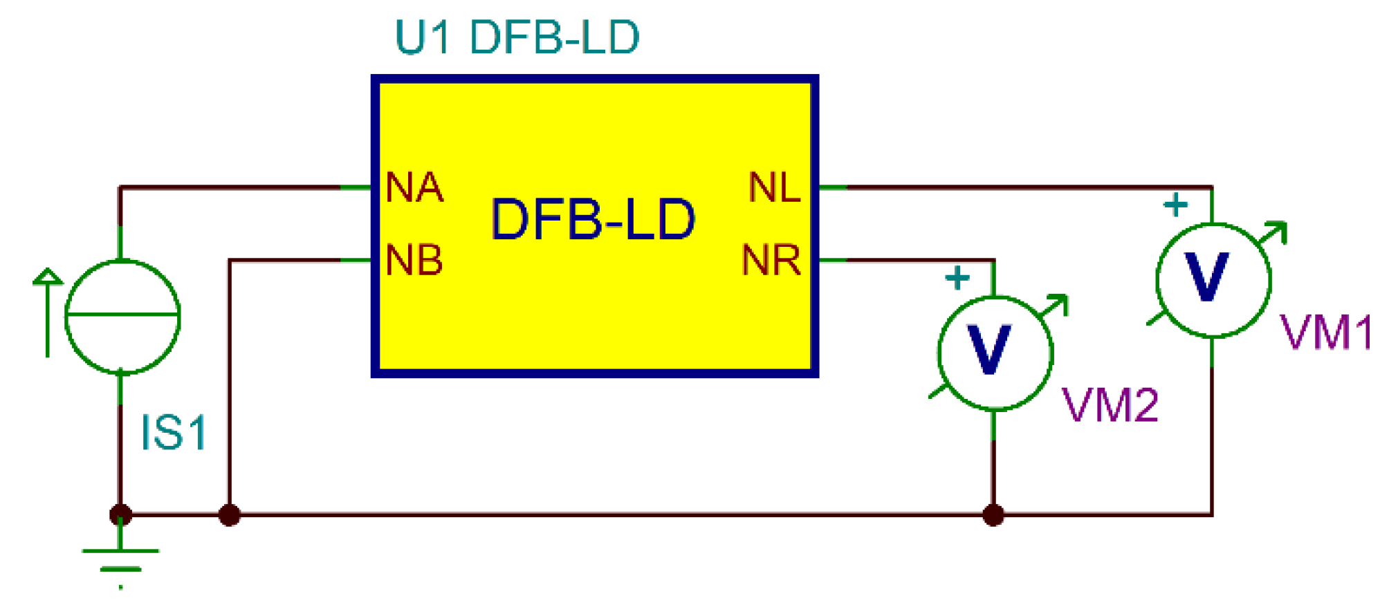
A test circuit shown in Figure 3 was designed for validating the macro-model of DFB-LD. The sweep range of IS1 was set within 0 to 100 mA with an accuracy of 0.1 mA, resulting in 1000 sampling points. Here the optical power is measured through a voltmeter, which is just an equivalent processing in a purely mathematical sense. The voltage obtained from measurement and the optical power of the laser model is only numerically equal, and the units of them are different.

2.2. Design of the Current Source

2.2.1. Schematic of the Circuit

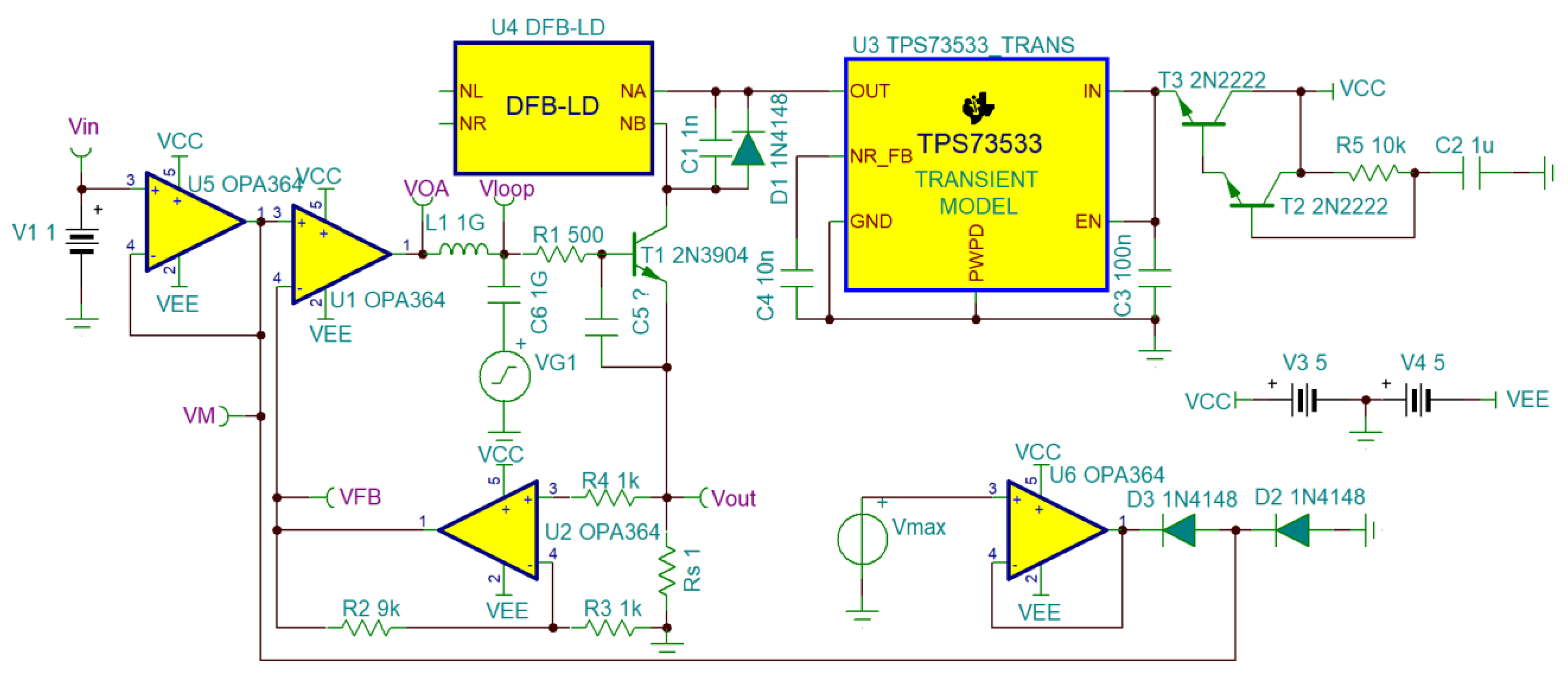
A float-ground type current source for laser driving was sketched in Figure 4. In order to make the simulation more realistic, the built macro-model of DFB-LD was introduced. A 500 Ω resistor (R1) was connected to the output of operational amplifier U1 to limit the maximum current flowing into the base of T1. The current supplied to the laser diode was sampled by a 1 Ω Z-Foil resistor (Rs) and amplified by operational amplifier U2. The adding of resistor R4 was to balance the input resistance of the non-inverting and inverting terminals of U2. The output of U2 was fed back to U1 and compared with the preset voltage of DAC2 (Vref). The result of the comparison causes the internal resistance of T1 to be automatically adjusted, thereby closing the negative feedback loop. The current outputted from the emitter of T1 was linearly regulated by Vref, leading to the expression as follows:
I s = V s R s = V r e f R 3 R s ( R 2 + R 3 ) .
Reverse surge, current spike and fast start-up current are harmful to the laser, so they should be avoided. While the laser power supply is turning off, a momentary reverse surge will be generated. The reverse biased high-speed switching diode (D1) is connected in parallel to the laser module to prevent the reverse surge from flowing into the cathode of the laser. Capacitor C1 can absorb a large amount of current spike which is caused mainly by the fluctuation of power supply [24,25]. Two series switching diodes (D2 and D3) connected to the non-inverting input of U1 act as a current limiter. In this way, the lower and upper threshold of the preset voltage, which confines the range of desired current, is clamped between 0 V and the output of DAC1 (Vmax), respectively. The soft-start of the laser driver is implemented by charging a capacitor (C2) through a resistor (R5). Meanwhile, the Darlington pair (T2 and T3) is gradually turned on and its emitter voltage rises smoothly until a stable value is reached. Voltage regulator U3 (TPS73533) converts the emitter voltage of T3 to a 3.3 V DC output with the maximum current of 500 mA. Although increasing the feedback coefficient of the feedback loop can improve the stability of the circuit, increase the input impedance, reduce the output impedance and expand the pass-band, there is a hidden danger of self-oscillation. To reduce the possibility of self-oscillation, capacitor C5 is connected between the base and emitter of T1 for loop compensation. In Section 4.2, the stability of the circuit with and without compensation will be discussed separately.

2.2.2. Deformation of the Circuit for Stability Analysis

The ratio of the output of the operational amplifier circuit to its input can be expressed as:
V o u t / V i n = V o u t / ( V i n + V i n ) = A o l / ( 1 + A o l β ) = A o l / ( 1 + A o l / β 1 )
where Vout represents the output of operational amplifier, Vin represents the input, Aol is open-loop gain, β is feedback factor and β1 is reciprocal of β. It can be seen from Equation (2) that the ratio of Aol to β1 is an important criterion for stability of the circuit. When the amplitudes of Aol and β1 are equal and the phases are opposite, the denominator of Equation (2) becomes zero, which indicates that self-oscillation will happen. The first order zero (pole) of the circuit will cause the amplitude-frequency characteristic curve to rise (fall) at a slope of 20 dB/decade. In view of that, analyzing the loop stability can be achieved simply by observing the closing rate of the amplitude-frequency curves of Aol and β1, that is, the slope when they cross each other. For this, the circuit shown in Figure 4 is slightly modified and redrawn in Figure 5.
Compared with Figure 4, a 1 GF capacitor (C6), a 1 GH inductance (L1) and an AC voltage source (VG1) with 1 V amplitude were added in the deformed circuit for maintaining the DC operating point while breaking the feedback loop. Due to the addition of the DC voltage source V1, the transistor T1 was biased near its actual operating point, thereby ensuring the correct AC analysis. By measuring the voltage of specific nodes and performing post-process using TINA-SPICE, the amplitude-frequency characteristic of Aol and β1 can be obtained and expressed by
A o l = V O A / ( V F B V M ) ,
β 1 = V l o o p / V F B .

2.3. User-Interface of the Laser Driver

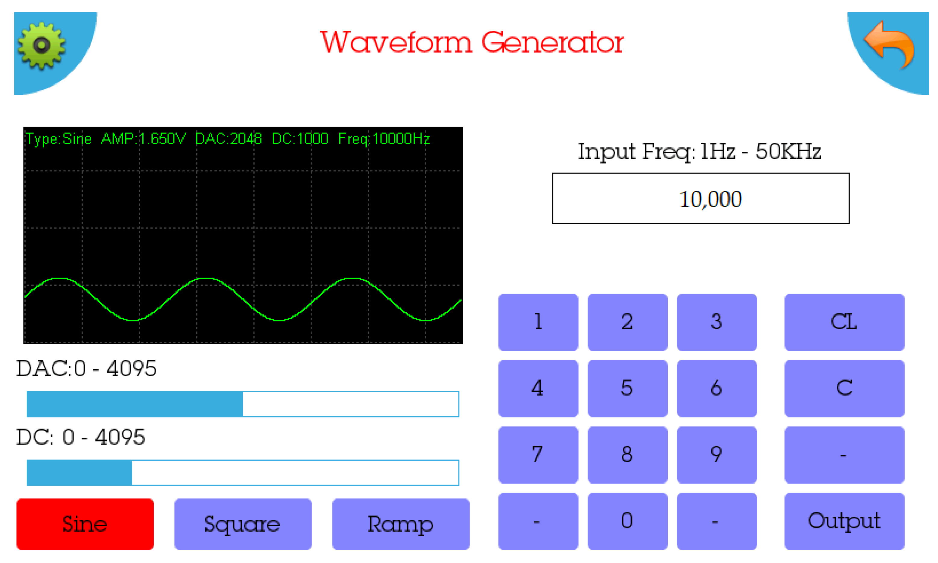
A graphical user-interface is designed based on emWin. A touch panel controller (TSC2046) embedded in RGB-LCD enables the setting of current to be realized by conveniently touching the screen. The upper left panel of the user-interface in Figure 6 shows the available waveform of the current, and two colored sliders below the panel are used to conveniently adjust the DC bias and the amplitude of the current. Three buttons deployed at the lower left can be clicked for choosing the type of current to be set. Conventionally, the sine or square wave is used for wavelength modulation while the ramp is for wavelength scanning. For the sake of distinction, the clicked button will be displayed in a different color from the other two. The frequency of the output signal is set by the keypad on the right and displayed on the text box above it. When the setting has been completed, the DACs of STM32H743 can be launched by pressing the “output” button on the keypad. A synthetic waveform composed of the modulating current, scanning current and DC bias will then be generated. The gear in the upper left corner is responsible for the screen-shot. The amplitude and the DC bias are expressed as a DAC value ranging from 0 to 4095 (12-bit resolution).

3. Application of the Laser Driver

3.1. Experimental Setup

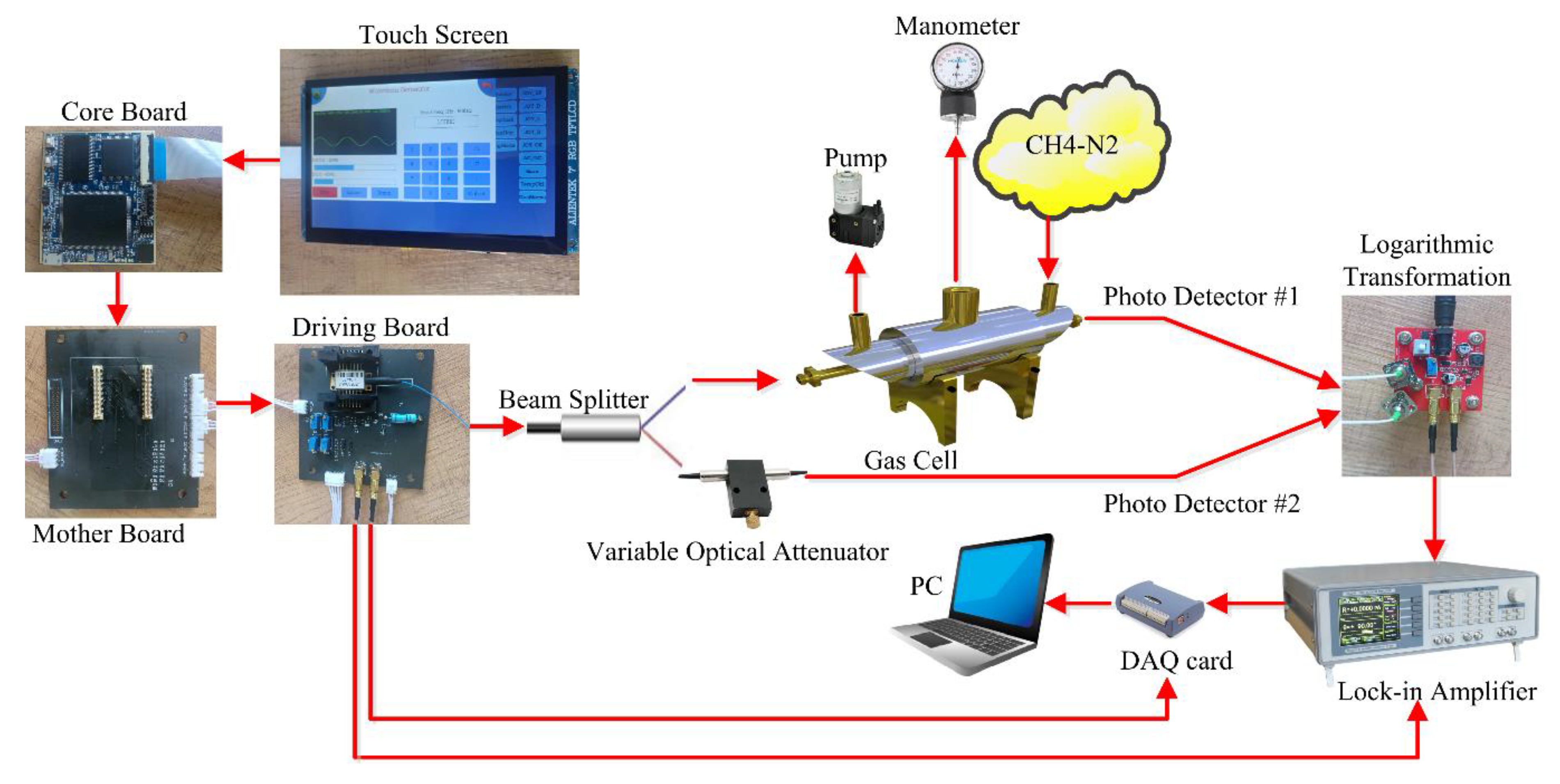
The layout of our apparatus, as shown schematically in Figure 7, is similar to that used in normal TDLAS-WMS-based trace gas detection, except for the adding of the aforementioned laser driver and a home-made circuit for logarithmic transformation and differential detection. As shown in this figure, the laser driver consists of a core board, a motherboard, a driving board and a touch screen. The motherboard is responsible for outputting the driving signal generated by the core board to the laser inserted on the driving board. The key to the operation of logarithmic transformation circuit is LOG114, which is a dedicated logarithmic amplifier for measuring low-level and wide dynamic range currents in communications, lasers, medical, and industrial systems. The referenced frequency of the lock-in amplifier is set to twice the modulating frequency, and the obtained second harmonic is digitized by a data acquisition (DAQ) card (USB-3210). The signal line draw from the laser driving board to the DAQ card is used to provide the time reference for the periodic scan. The other signal line connected to the lock-in amplifier is used to provide a referenced signal for the coherent detection. A PC programmed with LabVIEW software performs the averaging of the collected digital signals for 10 scan periods. For preparing CH4-N2 mixture with desired mole fraction, the mixing ratio of two cylinders filled with high-purity N2 and CH4 is regulated by a bank of mass flow controllers (Teledyne Hastings, HFC-302 with THPS-400 controller), with the total pressure measured by a vacuum pressure gauge and maintained at approximately 1.01 × 10⁵ Pa.

3.2. Basic Theory

Basic principles of absorption spectroscopy, such as the Beer–Lambert law and the modulation of the semiconductor laser have been well-described in earlier studies. The well-known contents will not be repeated here. Instead, we will focus on the improvements of TDLAS-WMS brought by logarithmic transformation and differential detection. After passing through the fiber beam splitter, the active beam experienced gas absorption and the auxiliary beam used as the reference were guided to detector D1 and D2, which generated the currents named I1 and I2:
I 1 ( t ) = K 1 I 0 ( t ) exp [ P S ( T ) g L ( ν ) χ L ] ,
I 2 ( t ) = K 2 I 0 ( t ) .
In Equation (5), P is the total pressure, S(T) is the line strength at temperature T, χ is the species mole fraction and L is the length of the optical path. K1 and K2 respectively represent the total gain of the active beam and the auxiliary beam, taking the splitting ratio of the modulated light intensity I0, transmittance of the gas cell and responsivity of the detector into account.
The circuit designed based on LOG114 was responsible for calculating the logarithmic ratio of I2 and I1, and generated the output as
V L O G O U T = 0.375 ( 1 + R 2 R 1 ) ln ( I 2 I 1 ) = 0.375 ( 1 + R 2 R 1 ) [ ln ( K 2 K 1 ) + P S ( T ) g L ( ν ) χ L ]
where R2 and R1 are resistors used to adjust the output amplitude to make it suitable for the subsequent signal processing. Theoretically, adjusting the VOA finely in the absence of a gas sample could entirely eliminate the DC bias that is related to K1 and K2, and thus obtains the optimal result. Actually, benefitting from the phase-sensitive detection of the lock-in amplifier, a tiny DC bias will not affect the final result. In the lock-in amplifier, VLOGOUT is first multiplied by the in-phase and orthogonal components of the referenced signal, and then the AC terms are filtered out from the product. The retained in-phase and orthogonal DC terms are written as
X in - phase = A m 2 cos ( γ ) P S ( T ) χ L C 2 ,
Y orthogonal = A m 2 sin ( γ ) P S ( T ) χ L C 2 .
In Equations (8) and (9), C2 is a Fourier coefficient of gL, which is shape function of the spectrum:
g L ( ν ) = k = 0 C k cos ( k ω c t ) .
In Equation (10), ν is the instantaneous wavenumber of laser and ωc is the angular frequency of wavelength modulation. For eliminating the influence of the detecting phase γ, the sum of square roots of Xin-phase and Yorthogonal is used to calculate R2f, which represents the amplitude of the second harmonic:
R 2 f = X in phase 2 + Y orthogonal 2 = A m 2 P S ( T ) χ L | C 2 | .
Further analysis had been carried out for the relationship between |C2| and χ. The result in Figure 8 shows that although χ increased by 25 times (400 ppm to 1%), the change of C2 is almost negligible. Except for C2, the remaining parameters in Equation (11) are fixed and independent of χ. Therefore, an approximately linear relationship is established between R2f and χ.

4. Results and Discussion

4.1. Simulations of the Current Source

4.1.1. Validation of the DFB-LD Model

P-I characteristic of the laser was simulated via DC sweep analysis using the test circuit shown in Figure 3. In Figure 9, it was clearly observed from the curve that while the injection current of the laser is less than a threshold (20 mA), the output optical power is extremely weak. The injection current then grows progressively, and the output optical power increases linearly in proportion to the injection current.

4.1.2. Stability Analysis without Compensation

The amplitude-frequency characteristic was simulated using the circuit shown in Figure 5. For comparing and analyzing the stability of the circuit with and without compensation, capacitor C5 was first removed and then added. As could be seen in Figure 10, the obtained curves of Aol and β1 cross each other with a slope of 40 dB/Decade. According to Equation (2), self-oscillation will occur around the frequency where the curves intersect. Although it is unclear whether the zero point on the curve of β1 originates from the parasitic capacitance of the transistor T1, it does not affect the stability analysis of the circuit and the formulation of a compensation strategy.
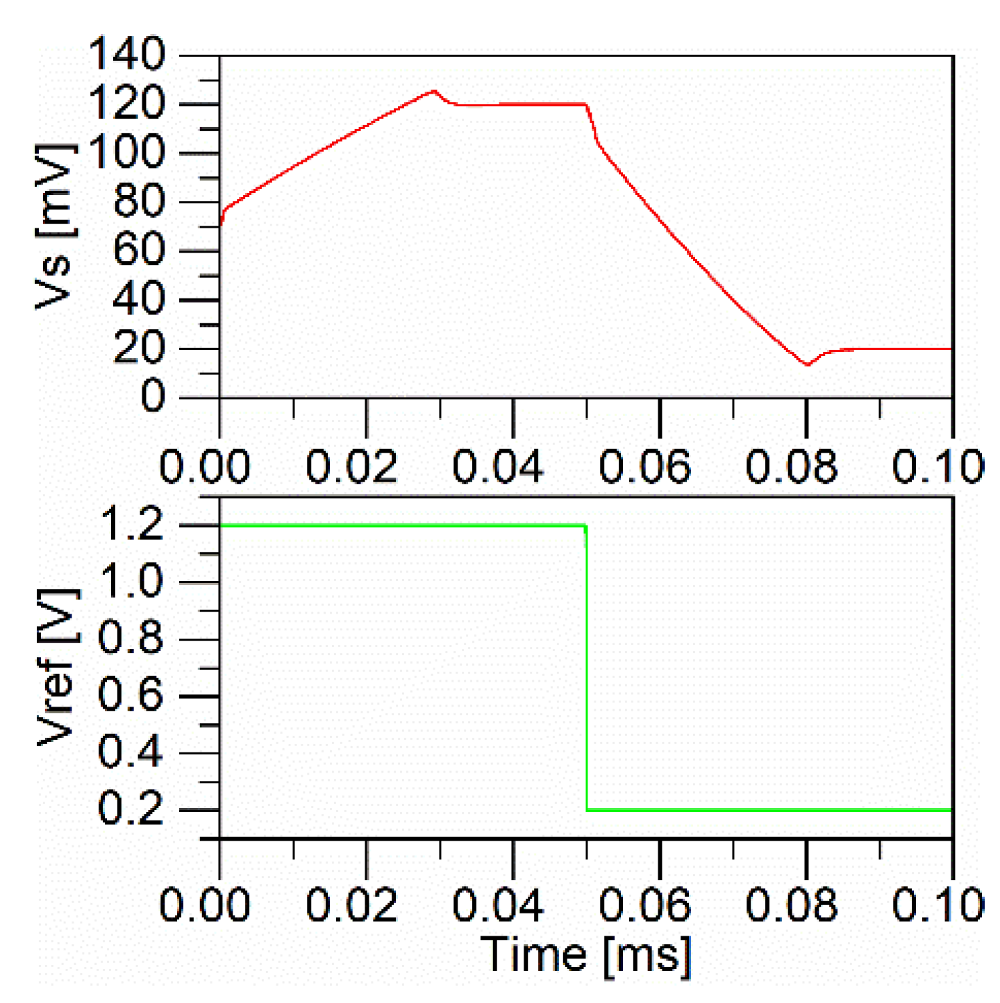
For a more intuitive perspective, a transient analysis was performed using the circuit shown in Figure 4. Vref was set to a 10 KHz square wave with 500 mv amplitude. The waveforms of the output node (Vs) and the input node (Vref) were recorded and shown in Figure 11, in which the oscillation was clearly depicted.

4.1.3. Stability Analysis with Compensation

Considering that the oscillation was caused by the rise of β1, a pair of zero-poles was added by the introduction of capacitor C5, from which the slope of β1 was compensated. In the simulation of the amplitude-frequency curve, we found that C5 with a capacitance greater than 1 uF can achieve the expected compensation effect, as shown in Figure 12.
In addition, it was found that the larger the capacitance, the more stable the circuit. However, the enhancement in stability was accompanied by a reduction in the output signal bandwidth. Therefore, considering the trade-off between circuit stability and signal bandwidth, the appropriate capacitance was finally determined to be 1 uF. Comparing the transient responses shown Figure 13 (capacitor C5 is added) and Figure 11 (capacitor C5 is removed), the effect of the compensation using C5 was obvious.

4.2. Gas Sensing Experiments

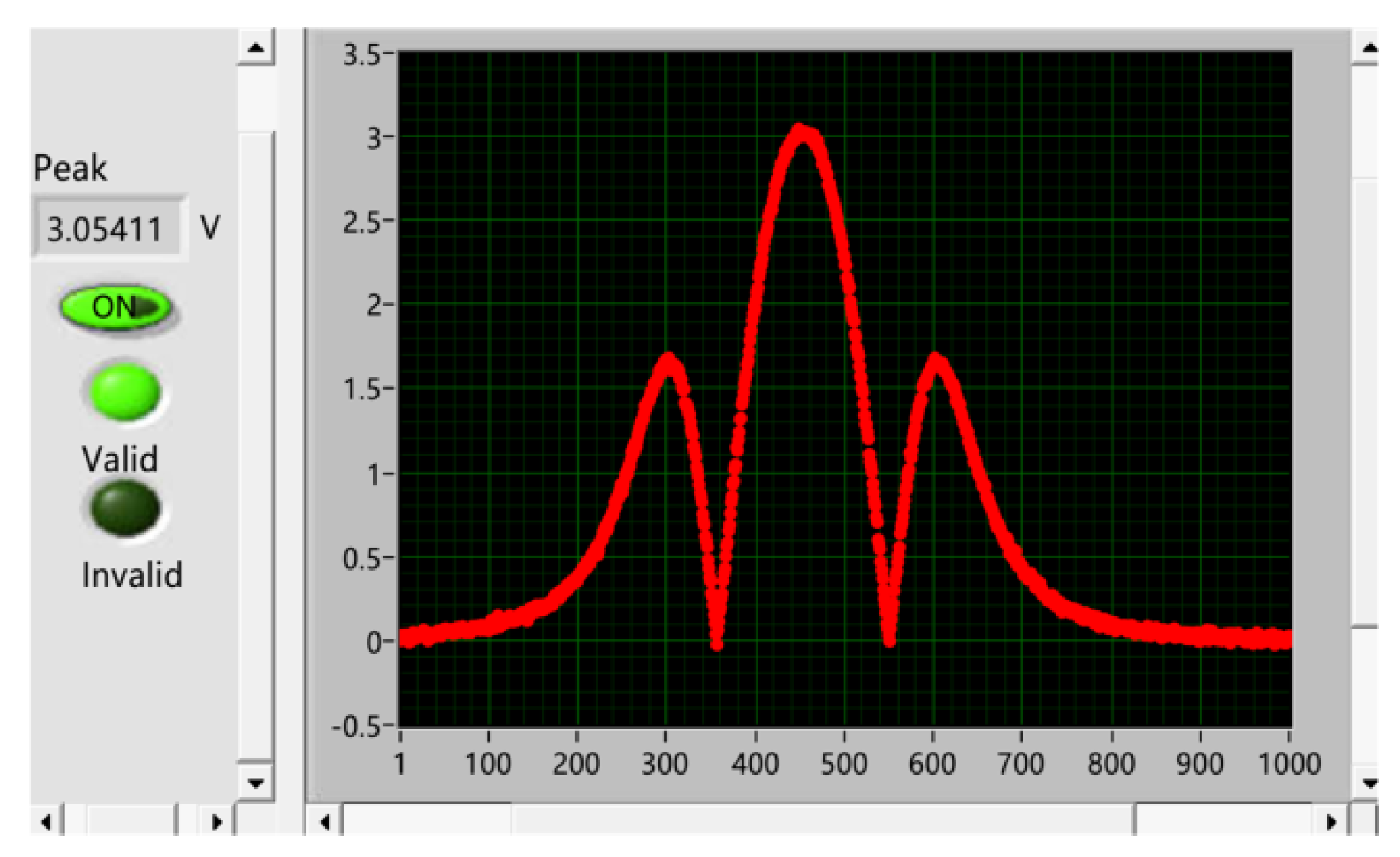
The experimental setup (see Figure 7) was verified by the results shown in Figure 14, Figure 15 and Figure 16 for the measurements of CH4, with the modulation index of lasing wavelength set to approximately 2.2 so that the largest possible amplitude of the second harmonic could be reached. Figure 14 gives an example of the recorded second harmonics. The output of the lock-in amplifier was continuously sampled by the data acquisition card. The program written in LabVIEW performed the averaging of the raw data. Through comprehensive consideration of both the signal-to-noise ratio and real-time requirement, the number of sampling points used for averaging was determined to be 10. The peak of the second harmonic obtained from the average using 10 samples is 3.05411 V. The wings of waveform are symmetrical and the DC offset is approximately zero, which is different from the traditional second harmonic detection.
To visualize the variation of detection results with sample concentrations, we present the peaks of harmonic signals obtained by measuring all samples with their concentrations ranging from 400 ppm to 1%. According to the fitting, the peak of harmonic has a highly linear dependence on the sample concentration, as predicted in Section 3.2. In Figure 15, a regression coefficient of R = 0.9976 was derived from the linear fitting described by
y = 15 . 0207 x ,
with y being the peak value of detector signal and x being the methane concentration.
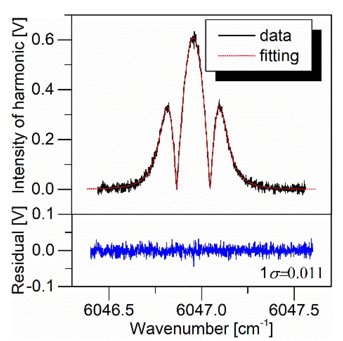
Strictly speaking, the detection limit of a gas sensor should be measured under the condition that the signal is equal to the noise. However, in a limited number of measurements, it is difficult to achieve equal signal and noise intensity. Instead, the detection limit can be deduced from the experimental result of a high-concentration sample, such as the 400 ppm methane sample in our case. According to the wavelength-current relationship curve of the LD measured in advance by the spectrum analyzer, the wavenumber corresponding to the data point of the harmonic signal was obtained through conversion. As shown in Figure 16, the peak of the signal corresponding to the 400 ppm sample is 0.609 V, while the standard deviation of noise obtained by the nonlinear fitting based on the Levenberg-Marquardt’s algorithm is 0.011 V, and the calculated SNR is 55.4 (0.609/0.011). Thus, when the signal is reduced to be equal to the noise, the corresponding concentration should be 7.2 ppm (400 ppm/55.4), which is the detection limit.
Some CH4 sensors that are applied in industry or reported in literature are summarized in Table 2. The PRMD series designed by Iseki et al. [26] is an ultra-light handheld device that uses laser echoes for remote measurement in industry. Asakawa et al. [27] determined the optimum total pressure for the detection of CH4 by experimental and theoretical approaches. The compact analyzer developed by Dong et al. [28] achieved a detection limit as low as 1.4 ppb due to the selection of the interband cascade laser (ICL) and the fundamental ν3 band as the light source and target absorption line. It should be emphasized that the effective optical lengths of the above sensors are 10 m, 29.91 m and 54.6 m, respectively. According to the Beer–Lambert law, if all of the absorption lengths are converted to the same 15.4 cm, the theoretical detection limits obtained by Iseki et al. and Asakawa et al. should become 32.5 ppm and 11.7 ppm, which are close to ours (7.2 ppm). Moreover, if the different absorption intensities of the selected spectral lines are taken into account, the gap between the detection limits obtained by us and Dong et al. under the same conditions will be narrowed further.

5. Conclusions

In this paper, the design of a laser driver implanted with an RTX5 system and emWin GUI was systematically described. Although some similar circuits had been revealed in previous studies, most of them focus on the application, while the stability of the circuit was rarely analyzed in depth. Here, TINA-SPICE software was used to analyze the stability of the laser drive circuit from the working principle of the operational amplifier. The graphical simulation curves intuitively pointed out the potential oscillation risk of the circuit and showed a significant effect of the compensation method. Our study thus offers a feasible strategy to treat, with the problems that may occur in the design, not only the laser drivers but also other circuit modules. Importantly, to make the simulation as realistic as possible, a macro model built upon the laser rate equation was used as the DFB-LD, which differs largely from the diodes involved in general studies. For validation, the home-made laser driver was introduced into the gas sensor which combines logarithmic transformation and TDLAS-WMS. Compared with the classic WMS-2f technology, because the logarithmic conversion circuit additionally brought a small amount of noise, it seems to have no advantage in terms of the detection limit. However, the symmetrical harmonic waveform and negligible DC offset are obvious evidence that the logarithmic transformation method eliminates the influence of light intensity modulation (IM) on WMS. We firmly believe that by lengthening the optical path, reducing the etalon effect, and optimizing the circuit, the SNR can be further increased and an ideal detection limit can be reached.

Author Contributions

Conceptualization and methodology, M.C.; software and validation, Y.W. and K.Z.; formal analysis and writing, S.Z. and D.L. All authors have read and agreed to the published version of the manuscript.

Funding

This research was funded by Natural Science Foundation of Inner Mongolia Autonomous Region (China), grant number 2018BS06004; National Natural Science Foundation (China), grant number 61963031; Scientific Research Project of Inner Mongolia University for the Nationalities (China), grant number NMDYB19065; Intelligent Agricultural equipment & technical team of Inner Mongolia Minzu University.

Institutional Review Board Statement

Not applicable.

Informed Consent Statement

Not applicable.

Data Availability Statement

Data available on request to the corresponding author.

Acknowledgments

We would also like to thank Lynn for language editing.

Conflicts of Interest

The authors declare that they have no conflict of interest.

Appendix A

* PSpice Model Editor—Version 17.2.0
*$
.SUBCKT DFB-LD NA NB NL NR
*    Name of the Subcircuit: DFB-LD
*    Name of the Ports: NA, NB, NL, NR
*       NA, NB: Electrical Ports of the Device
*           NA Positive electrode, NB Negative Electrode
*       NL, NR: Virtual Ports for Light Emitting
*         NL Left Port, NR Right Port
*model parameters BEGIN
** Different lasers can be simulated by modifying the following parameters **
.PARAM L=300UM
.PARAM W=1.5UM
.PARAM D=0.2UM
.PARAM GAM=1.20
.PARAM T=10ns
.PARAM BEATsp=5E-5
.PARAM ID=0
.PARAM G0=25000
.PARAM Ntr=1E24
.PARAM EPS=6E-23
.PARAM B=1E-16
.PARAM A=7.5E-41
.PARAM Rl=1E-8
.PARAM Rr=1E-8
.PARAM ALFA0=5000
.PARAM Q1=1.9998
.PARAM Q2=1.4391E-4
.PARAM LAMBDA=1.56UM
.PARAM Rat=1.2
.PARAM Ng=3.6
.PARAM N0=6.5E16
.PARAM Vbi=1.1
.PARAM EIT=2
.PARAM Rs=1E-5
.PARAM Cp=0pF
.PARAM Rd=1E15
.PARAM Csc0=0pF
*model parameters END
***** Modification of the following content is prohibited ******
*CONSTANTS
.PARAM ECHARGE=1.6021918E-19
.PARAM BOLTZMAN=1.3806226E-23
.PARAM EPS0=8.854214871E-12
.PARAM PI=3.1415926
.PARAM TWOPI={2.0*PI}
.PARAM PLANCK=6.626176E-34
.PARAM PLANCK2PI={PLANCK/TWOPI}
.PARAM TEMPR=300
.PARAM VT={BOLTZMAN*TEMPR/ECHARGE}
.PARAM LSPEED=2.99792458E8
*Convert m to um
.PARAM UL={L*1E6}
.PARAM UW={W*1E6}
.PARAM UD={D*1E6}
.PARAM UG0={G0*1E-6}
.PARAM UNtr={Ntr*1E-18}
.PARAM UEPS={EPS*1E18}
.PARAM UB={B*1E18}
.PARAM UA={A*1E36}
.PARAM UALFA0={ALFA0*1E-6}
.PARAM ULAMBDA={LAMBDA*1E6}
.PARAM UN0={N0*1E-18}
.PARAM UQ2={Q2*1E6}
.PARAM ULSPEED={LSPEED*1E6}
.PARAM Vact={UL*UW*UD}
.PARAM Cg={ULSPEED/Ng}
.PARAM CPL={PLANCK*Cg*Vact*Rat*ULSPEED*(1-Rl)/ULAMBDA/UQ2*0.8}
.PARAM CPR={PLANCK*Cg*Vact*Rat*ULSPEED*(1-Rr)/ULAMBDA/UQ2*0.2}
.PARAM Tph={Ng/(ULSPEED*(UALFA0+Q1/UQ2))}
.PARAM QV={ECHARGE*Vact}
.PARAM Cph={QV}
.PARAM Rph={Tph/QV}
.PARAM Nal={IF(ID<1,UNtr*((1.0/Tph/(Cg*GAM*UG0))+1.0),UNtr*EXP(1.0/Tph/(Cg*GAM*UG0)))}
.PARAM Vl={EIT*VT*LOG(Nal/UN0)}
.FUNC N(V) {UN0*EXP(V/EIT/VT)-1.0}
.FUNC Cd(V) {QV*UN0*EXP(V/EIT/VT)/(EIT*VT)}
.FUNC Csc(V) {IF(V<Vbi,Csc0/SQRT(1.0-V/Vbi),Csc0/SQRT(0.1))}
.FUNC G1(V,S) {IF(ID<1,UG0*(N(V)/UNtr-1.0)/(1.0+UEPS*ABS(S)),UG0*LOG(N(V)/Ntr)/(1.0+UEPS*ABS(S)))}
.FUNC G(V,S) {IF(N(V)<UNtr,0.0,G1(V,S))}
.FUNC In(V) {QV*N(V)/T}
.FUNC Ia(V) {QV*UA*N(V)**3}
.FUNC Isp(V) {QV*UB*N(V)**2}
.FUNC Ist(V,S) {QV*Cg*GAM*G(V,S)*ABS(S)}
* Circuit description of the electrical part
RRS NA NA1 {Rs}
RRd NA1 NB {Rd}
CCp NA1 NB {Cp}
*GCd NA1 NB VALUE={Cd(V(NA1)-V(NB))*DDT(V(NA1)-V(NB))}
*GCsc NA1 NB VALUE={Csc(V(NA1)-V(NB))*DDT(V(NA1)-V(NB))}
CCd NA1 NB {Cd(Vl)}
CCsc NA1 NB {Csc(Vl)}
GIn NA1 NB VALUE={In(V(NA1)-V(NB))}
GIa NA1 NB VALUE={Ia(V(NA1)-V(NB))}
GIsp NA1 NB VALUE={Isp(V(NA1)-V(NB))}
GIst NA1 NB VALUE={Ist(V(NA1)-V(NB),V(NS))}
* S circuit
GIsp1 0 NS VALUE={BEATsp*Isp(V(NA1)-V(NB))}
GIst1 0 NS VALUE={Ist(V(NA1)-V(NB),V(NS))}
CCph NS 0 {Cph}
RRph NS 0 {Rph}
* the optical output of the virtual port on the left
El NL 0 VALUE={CPL*V(NS)}
* the optical output of the virtual port on the right
Er NR 0 VALUE={CPR*V(NS)}
.ENDS
*$

References

  1. Liu, W.; Sun, J.; Xu, L.; Zhu, S.; Zhou, X.; Yang, S.; Dong, B.; Bai, X.; Lu, G.; Song, H. Understanding the noble metal modifying effect on In2O3 nanowires: Highly sensitive and selective gas sensors for potential early screening of multiple diseases. Nanoscale Horiz. 2019, 4, 1361–1371. [Google Scholar] [CrossRef]
  2. Liu, W.; Xu, L.; Sheng, K.; Zhou, X.; Dong, B.; Lu, G.; Song, H. A highly sensitive and moisture-resistant gas sensor for diabetes diagnosis with Pt@In2O3 nanowires and a molecular sieve for protection. NPG Asia Mater. 2018, 10, 293–308. [Google Scholar] [CrossRef] [Green Version]
  3. Krishnan, K.; Gauni, S.; Manimegalai, C.T.; Malsawmdawngliana, V. Ambient noise analysis in underwater wireless communication using laser diode. Opt. Laser Technol. 2019, 114, 135–139. [Google Scholar] [CrossRef]
  4. Ibrahim, D.G.A.; Yasui, T. High-precision 3D surface topography measurement using high-stable multi-wavelength digital holography referenced by an optical frequency comb. Opt. Lett. 2018, 43, 1758–1761. [Google Scholar] [CrossRef]
  5. Wang, Z.; Liu, Z.; Deng, Z.; Deng, W.; Jia, X. Phase extraction of non-stationary interference signal in frequency scanning interferometry using complex shifted Morlet wavelets. Opt. Commun. 2018, 420, 26–33. [Google Scholar] [CrossRef]
  6. Li, Y.; Wang, P.; Meng, F.; Yu, H.; Zhou, X.; Wang, H.; Pan, J. Investigation of the electronical and optical properties of quantum well lasers with slightly doped tunnel junction. Semiconductors 2018, 52, 2017–2021. [Google Scholar] [CrossRef]
  7. Li, B.; Zheng, C.; Liu, H.; He, Q.; Ye, W.; Zhang, Y.; Pan, J.; Wang, Y. Development and measurement of a near-infrared CH4 detection system using 1.654 μm wavelength-modulated diode laser and open reflective gas sensing probe. Sens. Actuators B Chem. 2016, 225, 188–198. [Google Scholar] [CrossRef]
  8. Sackinger, E.; Ota, Y.; Gabara, T.J.; Fischer, W.C. A 15-mW, 155-Mb/s CMOS burst-mode laser driver with automatic power control and end-of-life detection. IEEE J. Solid-State Circuits 2000, 35, 269–275. [Google Scholar] [CrossRef]
  9. Vladimir, L.; Vladimir, M.; Yurii, K.; Mikhail, B. Determination of the maximum temperature in a non-uniform hot zone by line-of-site absorption spectroscopy with a single diode laser. Sensors 2018, 18, 1608. [Google Scholar] [CrossRef] [Green Version]
  10. Guo, X.; Zheng, F.; Li, C.; Yang, X.; Li, N.; Liu, S.; Wei, J.; Qiu, X.; He, Q. A portable sensor for in-situ measurement of ammonia based on near-infrared laser absorption spectroscopy. Opt. Laser Eng. 2019, 115, 243–248. [Google Scholar] [CrossRef]
  11. Zheng, F.; Qiu, X.; Shao, L.; Feng, S.; Cheng, T.; He, X.; He, Q.; Li, C.; Kan, R.; Fittschen, C. Measurement of nitric oxide from cigarette burning using TDLAS based on quantum cascade laser. Opt. Laser Technol. 2020, 124, 105963. [Google Scholar] [CrossRef]
  12. Cheng, Y.; Pan, J.; Wang, Y.; Zhou, F.; Wang, B.; Zhao, L.; Zhu, H.; Wang, W. 40-Gb/s low chirp electro absorption modulator integrated with DFB laser. IEEE Photonics Technol. Lett. 2009, 21, 356–358. [Google Scholar] [CrossRef]
  13. Chen, C.; Newcomb, R.W.; Wang, Y. A trace methane gas sensor using mid-infrared quantum cascaded laser at 7.5 μm. Appl. Phys. B 2013, 113, 491–501. [Google Scholar] [CrossRef]
  14. Crosson, E.R. A cavity ring-down analyzer for measuring atmospheric levels of methane, carbon dioxide, and water. Appl. Phys. B 2008, 92, 403–408. [Google Scholar] [CrossRef]
  15. Klein, A.; Witzel, O.; Ebert, V. Rapid, time-division multiplexed, direct absorption- and wavelength modulation-spectroscopy. Sensors 2014, 14, 1497. [Google Scholar] [CrossRef] [Green Version]
  16. Goldenstein, C.S.; Strand, C.L.; Schultz, I.A.; Sun, K.; Jeffries, J.B.; Hanson, R.K. Fitting of calibration-free scanned-wavelength-modulation spectroscopy spectra for determination of gas properties and absorption lineshapes. Appl. Opt. 2014, 53, 356–367. [Google Scholar] [CrossRef]
  17. Sur, R.; Sun, K.; Jeffries, J.B.; Socha, J.G.; Hanson, R.K. Scanned-wavelength-modulation-spectroscopy sensor for CO, CO2, CH4 and H2O in a high-pressure engineering-scale transport-reactor coal gasifier. Fuel 2015, 150, 102–111. [Google Scholar] [CrossRef] [Green Version]
  18. Guo, Y.; Qiu, X.; Li, N.; Feng, S.; Cheng, T.; Liu, Q.; He, Q.; Kan, R.; Yang, H.; Li, C. A portable laser-based sensor for detecting H2S in domestic natural gas. Infrared Phys. Technol. 2020, 105, 103153. [Google Scholar] [CrossRef]
  19. Barbu, T.L.; Parvitte, B.; Zeninari, V.; Vinogradov, I.; Korablev, O.; Durry, G. Diode laser spectroscopy of H2O and CO2 in the 1.877-μm region for the in situ monitoring of the Martian atmosphere. Appl. Phys. B 2006, 82, 133–140. [Google Scholar] [CrossRef]
  20. Dudzik, G. Ultra-stable, low-noise two-stage current source concept for electronics and laser applications. IET Circuits Devices Syst. 2017, 11, 613–617. [Google Scholar] [CrossRef]
  21. Ray, A.; Bandyopadhyay, A.; De, S.; Ray, B.; Ghosh, P.N. A simple scanning semiconductor diode laser source and its application in wavelength modulation spectroscopy around 825 nm. Opt. Laser Technol. 2007, 39, 359–367. [Google Scholar] [CrossRef]
  22. TINA-SPICE Software. Available online: https://www.ti.com/tool/TINA-TI/ (accessed on 15 August 2019).
  23. Chen, W.; Yang, S.; Liu, S. Optoelectronic Devices Circuit Model and the Circuit-Level Simulation of OEIC; National Defense Industry Press: Beijing, China, 2001; pp. 106–109. ISBN 7118023302. (In Chinese) [Google Scholar]
  24. Xiao, H.; Zou, W.; Fu, Y.; He, X.; Gan, Y. Design of diode laser output power auto control system. Appl. Laser 2004, 24, 165–168. (In Chinese) [Google Scholar] [CrossRef]
  25. Fu, Y.; Zou, W.; Xiao, H.; Gan, Y. Optic power control of LD drive circuit. Infrared and Laser Eng. 2005, 34, 626–630. (In Chinese) [Google Scholar] [CrossRef]
  26. Iseki, T. A portable remote methane detector using an InGaAsP DFB laser. Environ. Geol. 2004, 46, 1064–1069. [Google Scholar] [CrossRef]
  27. Asakawa, T.; Kanno, N.; Tonokura, K. Diode laser detection of greenhouse gases in the near-infrared region by wavelength modulation spectroscopy: Pressure dependence of the detection sensitivity. Sensors 2010, 10, 4686. [Google Scholar] [CrossRef] [PubMed] [Green Version]
  28. Dong, L.; Li, C.; Sanchez, N.P.; Gluszek, A.K.; Griffin, R.J.; Tittel, F.K. Compact CH4 sensor system based on a continu-ous-wave, low power consumption, room temperature interband cascade laser. Appl. Phys. Lett. 2016, 108, 011106. [Google Scholar] [CrossRef] [Green Version]
Figure 1. Flow chart of the code for regulating the laser driver.
Applsci 12 05883 g001
Figure 2. The internal equivalent circuit (left) and sub-circuit symbol (right) of a DFB-LD.
Applsci 12 05883 g002
Figure 3. Test circuit of DFB-LD.
Applsci 12 05883 g003
Figure 4. The float-ground type current source.
Applsci 12 05883 g004
Figure 5. Deformation of the current source for analyzing loop stability.
Applsci 12 05883 g005
Figure 6. Screenshot of user-interface of the laser driver.
Applsci 12 05883 g006
Figure 7. Schematic diagram of the experimental setup.
Applsci 12 05883 g007
Figure 8. Absolute value of C2 for different CH4 mole fractions (400 ppm to 1%).
Applsci 12 05883 g008
Figure 9. The simulated changing of optical power versus the injection current in the range of 0 to 100 mA with 0.1 mA accuracy.
Applsci 12 05883 g009
Figure 10. Simulated amplitude-frequency curves of Aol and β1 (capacitor C5 was removed).
Applsci 12 05883 g010
Figure 11. Transient response of the current source (capacitor C5 was removed).
Applsci 12 05883 g011
Figure 12. Amplitude-frequency characteristic curves of Aol and β1 with different values of C5.
Applsci 12 05883 g012
Figure 13. Transient response of the current source when C5 equals 1 uF.
Applsci 12 05883 g013
Figure 14. Waveform of second harmonic for 0.2% CH4 buffered by N2.
Applsci 12 05883 g014
Figure 15. Linear dependence of the harmonic on CH4 mole fraction.
Applsci 12 05883 g015
Figure 16. Measured data and its fitting of the harmonic for 400 ppm CH4.
Applsci 12 05883 g016
Table 1. Summary of the electric symbols in the equivalent circuit of DFB-LD.
SymbolsDescription
Rsparasitic resistor in series
Cpparasitic capacitor in parallel
Rdparasitic leakage resistor
Rpha constructed resistor with the resistance of kT/q2
(k the Boltzmann constant, T the temperature and q the electric charge)
Cddiffusion capacitor
Cscspace-charge capacitor
Klthe ratio of the optical power emitted from the left facet of the optical resonator to the photon density
Krthe ratio of the optical power emitted from the right facet of the optical resonator to the photon density
Betaspontaneous emission coefficient
NApositive end of laser electrical ports
NBnegative end of laser electrical ports
NLvirtual port on the left facet of the optical resonator
NRvirtual port on the right facet of the optical resonator
Table 2. Examples of the TDLAS-based CH4 sensors.
Ref.Detection Limit
(ppb)
Optical Lengths
(m)
Laser SourceLine Position
(cm−1)
[26]50010DFB-LD6046.95
[27]6029.91DFB-LD6046.95
[28]1.454.6DFB-ICL3038.50
Publisher’s Note: MDPI stays neutral with regard to jurisdictional claims in published maps and institutional affiliations.