Article

Quantum Dot-Based White Organic Light-Emitting Diodes Excited by a Blue OLED

Department of Electro-Optical Engineering, National Formosa University, Huwei, Yunlin 63208, Taiwan
*
Author to whom correspondence should be addressed.
Appl. Sci. 2022, 12(13), 6365; https://doi.org/10.3390/app12136365
Submission received: 16 May 2022 / Revised: 18 June 2022 / Accepted: 21 June 2022 / Published: 22 June 2022
(This article belongs to the Section Optics and Lasers)

Abstract

:
In this study, white organic light-emitting diodes (OLEDs) consisting of red quantum dots (RQD) and green quantum dots (GQD) were investigated. These are the most exciting new lighting technologies that have grown rapidly in recent years. The white OLED development processes used consisted of the following methods: (a) fabrication of a blue single-emitting layer OLED, (b) nanoimprinting into QD photoresists, and (c) green and red QD photoresists as color conversion layers (CCL) excited by blue OLEDs. To fabricate the blue OLED, the HATCN/TAPC pair was selected for the hole injection/transport layer on ITO and TPBi for the electron transport layer. For blue-emitting material, we used a novel polycyclic framework of thermally activated delayed fluorescence (TADF) material, ν-DABNA, which does not utilize any heavy metals and has a sharp and narrow (FWHM 28 nm) electroluminescence spectrum. The device structure was ITO/HATCN (20 nm)/TAPC (30 nm)/MADN: ν-DABNA (40 nm)/TPBi (30 nm)/LiF (0.8 nm)/Al (150 nm) with an emitting area of 1 cm × 1 cm. The current density, luminance, and efficiency of blue OLEDs at 8 V are 87.68 mA/cm2, 963.9 cd/m2, and 1.10 cd/A, respectively. Next, the bottom emission side of the blue OLED was attached to nanoimprinted RQD and GQD photoresists, which were excited by the blue OLED in order to generate an orange and a green color, respectively, and combined with blue light to achieve a nearly white light. In this study, two different excitation architectures were tested: BOLED→GQD→RQD and BOLED→RQD→GQD. The EL spectra showed that the BOLED→GQD→RQD architecture had stronger green emissions than BOLED→RQD→GQD because the blue OLED excited the GQD PR first then RQD PR. Due to the energy gap architectures in BOLED-GQD-RQD, the green QD absorbed part of the blue light emitted from the BOLED, and the remaining blue light penetrated the GQD to reach the RQD. These excited spectra were very close to the white light, which resulted in three peaks emitting at 460, 530, and 620 nm. The original blue CIE coordinates were (0.15, 0.07). After the excitation combination, the CIE coordinates were (0.42, 0.33), which was close to the white light position.

1. Introduction

Flourishing white organic light-emitting diodes (OLEDs) are vital for future solid-state lighting devices and full-color displays [1]. The quantum dot (QD) OLED is one of the most popular OLEDs today because of its wide color space, wide viewing angle, and other benefits it provides [2]. The emission wavelengths of QDs can be adjusted by the altering the size of the QDs, and the quantum efficiency of their photoluminescence (PL) is high. They have a high absorption capacity at blue wavelengths and offer high conversion efficiency. Therefore, QDs can be used as perfect color conversion materials [3]. Due to the feasibility of the solution process of the QD layer, the color tuning of the QD material, the narrow FWHM of the emission spectrum, the high luminous efficiency, and the fact that QDs are inorganic materials means that they have a useful life that is longer than organic ones. QD materials have proven that their advantages have great potential for next-generation displays. As a color conversion material, QDs can be used as a color enhancement film (QDEF) in the backlight of an LCD screen or as a quantum dot color filter (QDCF) in an OLED screen to expand the screen’s color space [4,5]. A QD has discrete electronic states, like natural atoms, and its electronic wave function is somewhat similar to that of an atom. They are often referred to as artificial atoms [6]. QDs are widely applicable in a variety of fields due to their highly tunable properties. They could potentially be used in electronic technologies and display technology, for example, in solar cells, photodetectors, photodiodes, field-effect transistors, biological systems, flat-panel TV displays, digital cameras, mobile phones, and gaming equipment [7,8,9,10,11,12,13].
Many studies are being conducted on quantum dot units, yet few provide information on how the device or process architecture might contribute to the overall color space [14]. For example, Maojun Yin et al., from Jilin University, used CdSe/ZnS quantum dot material mixed with polymethylmethacrylate (PMMA) to create a separate composite film to convert a blue OLED to a white color, producing a white OLED with a maximum luminance of 10,250 cd/m2 and maximum current efficiency of 20.6 cd/A. In the case of white the OLED, the CIE coordinates shifted only from (0.291, 0.406) at 4 V to (0.288, 0.405) at 8 V. This showed a relatively high degree of spectral stability under voltage variations. In addition, by integrating ordered microcylinder arrays with down-conversion films by transfer imprint, the viewing characteristics, and light extraction performance were improved for white OLEDs [15]. HyoJun Kim et al. from Yonsei University, South Korea, used red and green quantum dot materials mixed with PGMEA and positive photoresist and exposed and developed the technology on a glass substrate to create a full-color OLED display. Compared with conventional OLED displays, after using QDs, the light intensity of the white OLED in the red and green sub-pixels increased by 32.1% and 9.6%, respectively. After that, an air-gapped bridge structure was added between the OLED and the QDs to achieve a full internal reflection (FIR) that performed an optical cycle to improve the QDs’ color conversion efficiency. The light intensity of the red and green sub-pixels increased by 58.2% and 16.8%, respectively, and due to the narrow emission spectrums of the QDs, the color space of the proposed OLED screen increased by 65%, from 5% to 75.9% [16]. Jung Hyuk Im et al. Hongik University in South Korea investigated the color conversion properties of QDs/OLEDs using the microcavity effect, with OLEDs fabricated on WO3/Ag/WO3 (WAW) anodes. WAW devices with different thicknesses have different color coordinates due to the resonant cavity effect. As an example, when the WO3 material possesses 120 nm of thickness, its coordinates for white light are (0.31, 0.37) [17].
QDs exhibit pure and saturated colors in the visible spectrum, as well as narrow bandgaps and high photoluminescence efficiency due to quantum confinement. Furthermore, modifying the particle surface can greatly enhance the fluorescence efficiency and, in particular, the structural stability of the nanocrystals. By combining these characteristics with the distinctive properties of organic materials, such as flexibility and ease of processing, low-cost hybrid white-emitting devices with improved lifetimes and color stability can be developed [18,19]. Recently, quantum dot materials, such as CdSe/ZnS, have also been used in LED backlights and displays. CdSe/ZnS colloidal QDs possess a high quantum yield and good photostability at room temperature. This makes them an excellent choice for the lighting industry, and they have been extensively studied [20,21,22]. In many optoelectronic devices, quantum dots (QDs) are used as phosphors to absorb light in order to convert it into low-energy light in long wavelengths, since they exhibit excellent optical properties. The performance of QD-OLEDs depends on an efficient injection of charge carriers into the QDs from the electrodes. The choice of organic or inorganic semiconductors should be based on their energy levels in comparison to QDs. In the fabrication of OLEDs with quantum dots (QDs), alternate fabrication technologies have been suggested in order to achieve high efficiency, high stability, high durability, and cost-effectiveness [23,24,25].
The advantages of organic materials in light-emitting devices, including displays, comprise their ability to be deposited on glass and flexible substrates and their dazzling brightness. However, if organic materials were combined with quantum dots’ unique properties, a more effective device could be created. QD-OLEDs based on QDs’ CdSe/ZnS have been the subject of numerous attempts to increase performance by optimizing the device architecture. In this study, the electrical and optical properties of BOLEDs and WOLEDs were investigated using current density–voltage, luminance–voltage, photoluminescence (PL), and electroluminescence measurements. To develop a quantum dot-based WOLED, the following three approaches were carried out: (a) fabrication of a blue single-emitting layer OLED [ITO/HATCN (20 nm)/TAPC (30 nm)/MADN: ν-DABNA (40 nm)/TPBi (30 nm)/LiF (0.8 nm)/Al (150 nm)], (b) nanoimprinting into QD photoresists, and (c) green and red QD (CdSe/ZnS) photoresists as color conversion layers (CCL) excited by blue OLEDs. The red and green QD (CdSe/ZnS) photoresists were used as a color conversion layer and excited by a blue OLED to form white light. The study also strived to establish the exquisite architecture (BOLED→RQD→GQD) for the WOLED.

2. Experimental Details

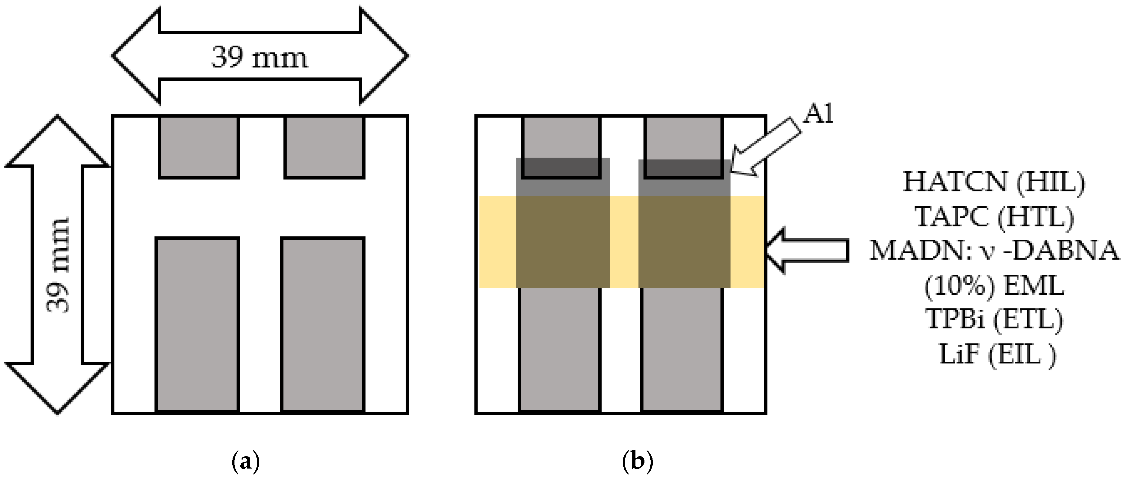
2.1. Blue OLED Device Fabrication

For the substrate, ITO (indium tin oxide) glass was used. ITO’s sheet resistance was about 12 Ω/☐, and the effective emitting area was about 1 cm × 1 cm. Manufacturing for both blue OLEDs (BOLEDs) and white OLEDs (WOLEDs) was carried out in the following processes. To fabricate the blue OLED, the ITO patterns were engraved at the beginning, as shown in Figure 1a. To ensure the substrate was thoroughly cleaned, the following procedures were followed: the substrate was soaked in acetone, isopropanol, and deionized water sequentially then cleaned using an ultrasonic vibration cleaner for 30 min. After a while, the substrate was blown dry with 99% pure nitrogen (N2) and then put into an oven for 10 to 20 min to bake at a temperature of 80 °C. Hence, moisture residue on the substrate could be avoided. In the next step, the organic and metallic layers were deposited using a thermal vacuum deposition system (at 8 × 10⁻⁶ torr).
The organic material was deposited on the substrate at a rate of 0.8–1.0 Å/s in the order of hole injection layer/hole transport layer/emitting layer/electron transport layer (HIL/HTL/EML/ETL). The deposition area is shown in Figure 1b. The metal materials LiF and Al were deposited on the substrate at a rate of 0.1 Å/s and 10 Å/s, respectively. Following that, blue OLEDs were fabricated.

2.2. White OLED Device Fabrication

The red quantum dot photoresist (RQD PR) and green quantum dot photoresist (GQD PR) materials (purchased from Yeh-Ji Industrial Co., Ltd., Taiwan) were spin coated on glass substrates at 600 rpm and 500 rpm, respectively, for 60 s each, as shown in Figure 2. After spin coating, the RQD PR and GQD PR glass substrates were put on a hot plate for 2 min to prebake at a temperature of 80 °C. Once the baking was completed, the substrate was exposed to a 500 mJ ultra-violet (UV) exposure machine for 50 s. Once the exposure was performed, the substrate was placed on a hot plate and baked at 80 °C for 20 min to cure the QD PR completely. In addition, commercially available patterned sapphire was used for nanoimprinting the QD photoresist to make the surface of the photoresist rougher. Lastly, nanoimprinted RQD and GQD photoresists were attached to the blue OLED device, the Keithley 2400 (power supply and current–voltage measurement) was used to bias the blue OLED, and the Spectra Scan PR 650 Spectral Colorimeter was used to measure its luminance and spectra. Thus, the current–luminance–voltage (I–L–V) characteristic for white OLEDs was obtained.

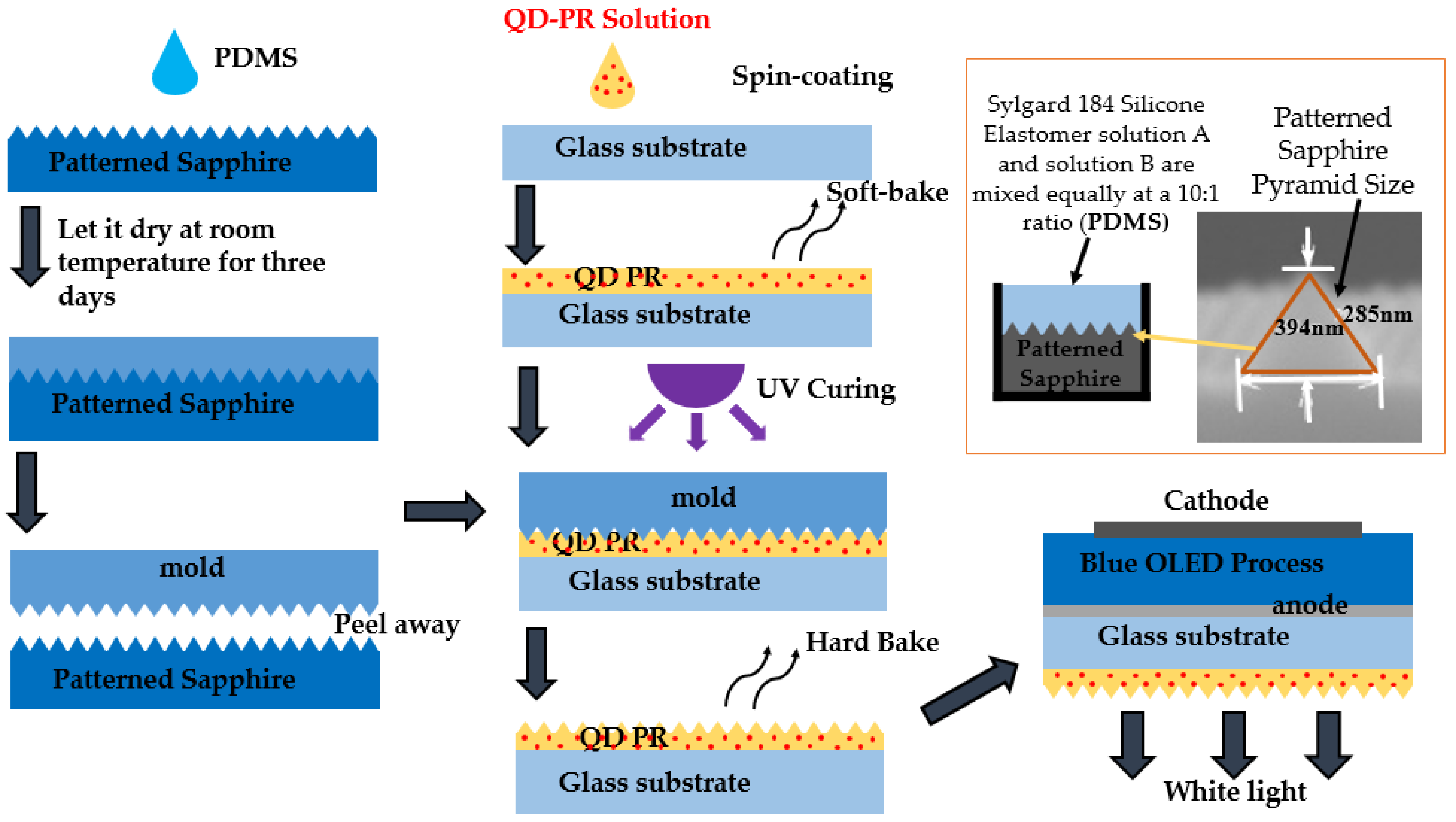
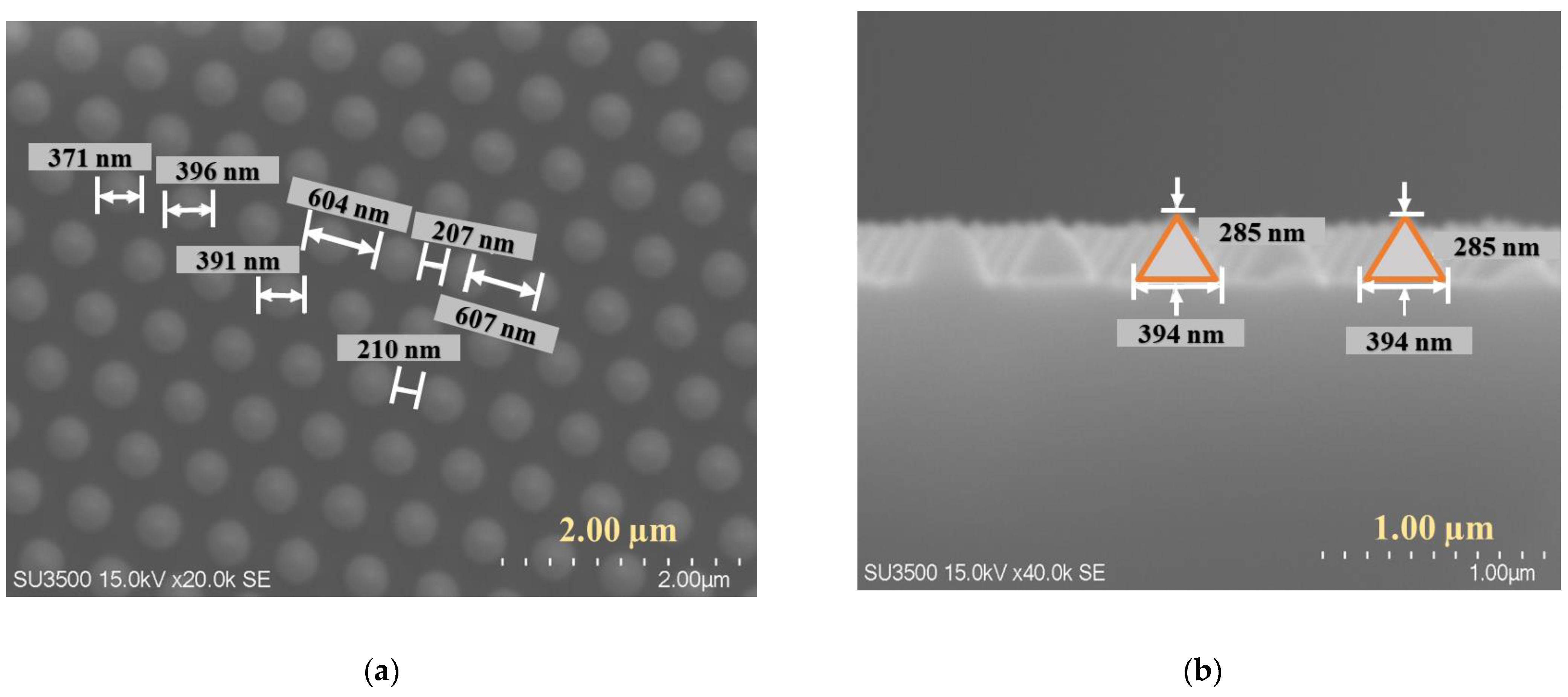
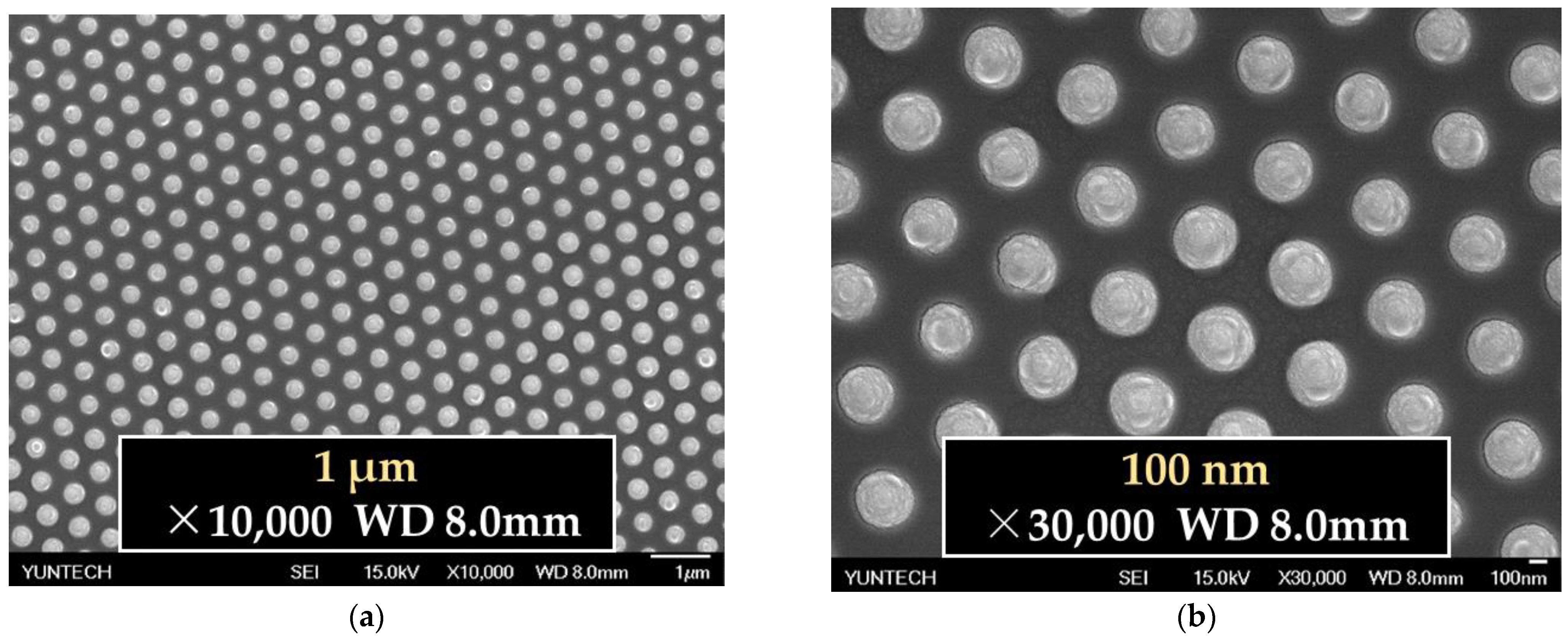
2.3. Nanoimprinting on QD Photoresists

For developing the nanoimprint onto a QD photoresist, patterned sapphire was used as a master mold. In the first process, Sylgard 184 Silicone Elastomer solution A and solution B were mixed equally at a 10:1 ratio to develop polydimethylsiloxane (PDMS). A mixed PDMS solution was dropped onto the patterned sapphire for 15 min, and the air bubbles were removed using a vacuum dryer before leaving it at room temperature for three days to cure. When the process was completed, the PDMS mold was peeled away from the patterned sapphire. Eventually, the PDMS mold was attached to the spin-coated QD PR glass substrates and exposed for 50 s using a 500 mJ UV exposure machine. By following the procedure, the nanoimprinting on the QD photoresist was successfully achieved. Figure 3 illustrates the entire fabrication process.
The scanning electron microscope (SEM) top view and cross-section view along with the pyramid shape of the patterned sapphire are shown in Figure 4a,b, respectively. The bottom of the pyramid measured about 394 nm, the height was about 285 nm, and the spacing was about 200 nm. Figure 5 shows the photos of the patterned sapphire surface using a SEM: (a) the picture has been magnified 10,000 times and (b) the picture has been magnified 30,000 times.

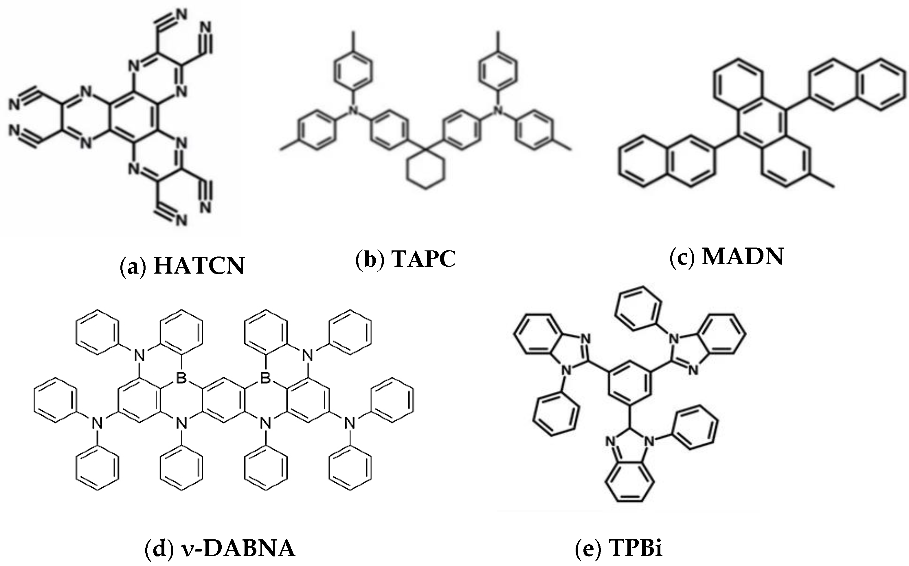
2.4. Material Details

Using thermally activated delayed fluorescence (TADF) material is a promising method to produce efficient blue electroluminescence. Recent studies have revealed that TADF materials can convert all electrogenerated singlets and triplets into light [26,27]. Since TADF OLEDs are pure organic molecules, they avoid costly noble metals. Apart from the blue emitters, host materials are also crucial for the performance of an OLED [28]. Device luminous efficiency is directly affected by luminescent material performance. Consequently, a lot of OLED research is devoted to the behavior of luminescent materials, such as their electroluminescence (EL) efficiency, their radiative lifetimes, and their color purity. Furthermore, a variety of matching auxiliary materials have been studied and developed, such as hole transport materials, electron transport materials, exciton blocking materials, and host materials, to increase the performance of the luminescent materials [29]. It is predicted that the high-efficiency TADF blue light material will reduce mobile device power loss, and extend battery life and heat activation if it becomes commercially available in the future. TADF materials were used to fabricate blue OLEDs in this study. The chemical structure of the materials is shown in Figure 6.
Dipyrazino[2,3-f:2′,3′-h]quinoxaline-2,3,6,7,10,11-hexacarbonitrile (HATCN) was employed as the hole injection layer (HIL) with HOMO = 9.5 eV and LUMO = 4.5 eV, 1,1-Bis[(di-4-tolylamino)phenyl]cyclohexane (TAPC) was employed as the hole transport layer (HTL) with HOMO = 5.5 eV and LUMO = 2.0 eV, 2-Methyl-9,10-bis(naphthalen-2-yl)anthracene (MADN) was employed as the host emitting material with HOMO = 6.4 eV and LUMO = 3.3, N7,N7,N13,N13,5,9,11,15-octaphenyl-5,9,11,15-tetrahydro-5,9,11,15-tetraaza-19b,20b-diboradinaphtho[3,2,1-de:1′,2′,3′-jk]pentacene-7,13-diamine (ν-DABNA) was employed as the dopant emitting material with HOMO = 5.4 eV and LUMO = 2.8 eV, and 2,2′,2′′-(1,3,5-Benzinetriyl)-tris(1-phenyl-1-H-benzimidazole) (TPBi) was employed as the electron transport layer (ETL) with HOMO = 6.2 eV and LUMO = 2.7 eV. The organic materials were purchased from Yeh-Ji Industrial Co. Ltd., Taiwan.

3. Results and Discussion

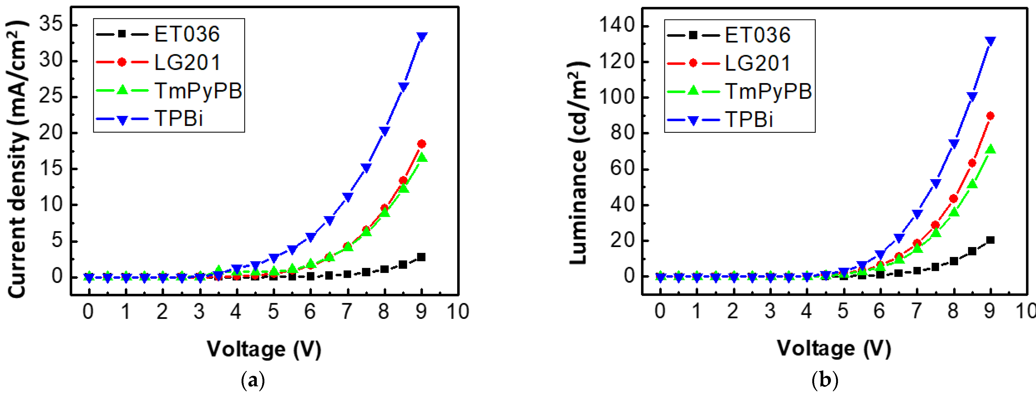
3.1. The Comparison of Electron Transport Layer Materials

As part of the fabrication of the blue OLED, an experiment was conducted to determine the material that was most suitable for the electron transport layer (ETL). Several ETL materials were considered, such as X = ET036, LG201, TmPyPB, and TPBi, and the current–voltage and luminance characteristics of OLEDs with these materials were compared. The device structure was ITO/PEDOT: PSS/Poly-TPD/mCP (15 nm)/MADN: ν-DABNA (50 nm)/X/LiF (0.8 nm)/Al (150 nm). Here, Poly-TPD was dissolved in chlorobenzene into a solution with a concentration of 5 mg/mL. After thorough stirring, it was spin coated on the top of PEDOT: PSS was used for the hole transport layer. The energy band diagram of the device is shown in Figure 7. Table 1 shows the structural parameters of the devices for modulating the ETL materials. Figure 8 shows the (a) current density-voltage and (b) the luminance–voltage characteristic of the blue OLEDs that modulated various ETL materials. As shown in Figure 8, compared with other ETL materials, TPBi had a better effect on electron injection, thereby increasing the probability of hole–electron recombination, and improving the luminance of the OLEDs. It could be seen that the current density and luminance were higher with TPBi as the ETL material. At a voltage of 8 V, the current density was 20.39 mA/cm2 and the luminance was 89.55 cd/m2.

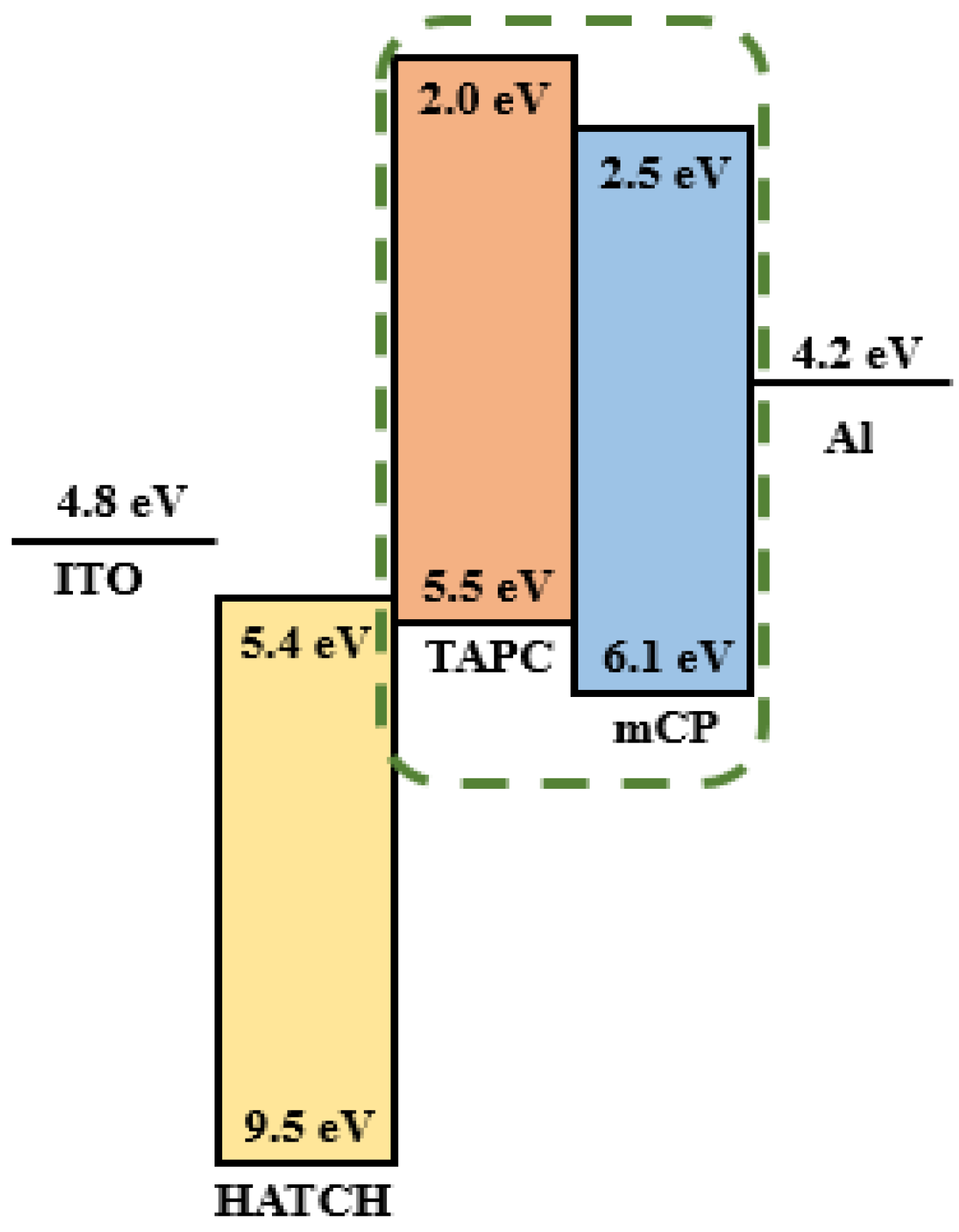
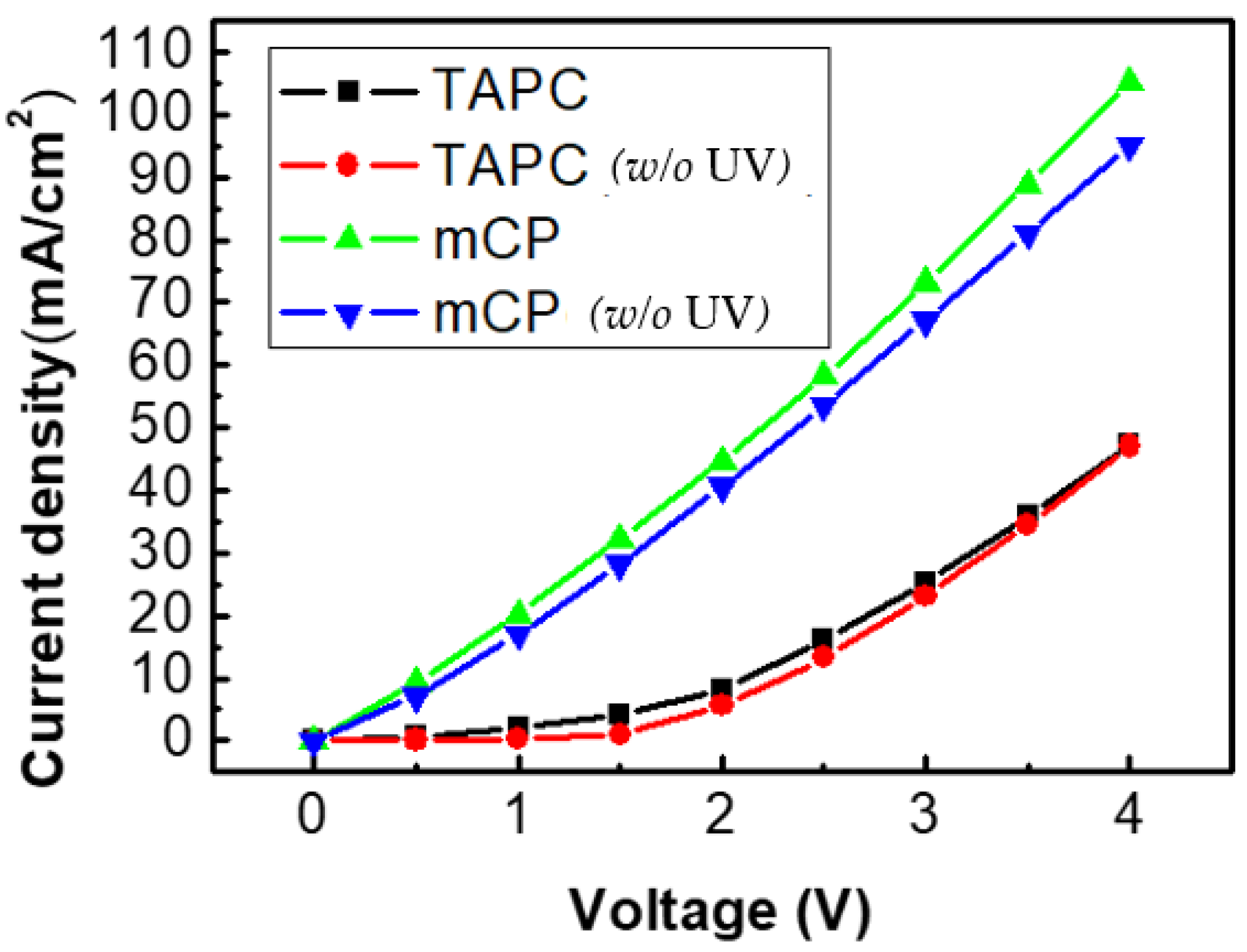
3.2. The Comparison of Hole Transport Layer Materials

In this work, HATCN was selected for the hole injection layer (HIL), with thickness fixed at 10 nm. The device structure was ITO/HATCN (10 nm)/X/LiF/Al (150 nm) where different hole transport layers (HTL) were employed, X = TAPC or mCP. The effect of UV ozone treatment on the ITO substrate on the electro-optical properties of blue OLEDs was discussed. The energy band diagram of the device is shown in Figure 9. Table 2 shows the structure parameters of hole-only devices with different HTL materials. Figure 10 shows the current density–voltage characteristics. By comparing the characteristics in Figure 10, it was evident that when using either mCP or TAPC as HTL, the current density without UV ozone treatment was slightly lower than those with UV ozone treatment.
Because HATCN is one of the hexaazatriphenylene derivatives with strong oxidizing properties, it had a cleaning effect on the contaminated ITO surface and could effectively modify the ITO surface. The hole-only device with HATCN/mCP had a higher current density than those with HATCN/TAPC. However, if the hole current density of HATCN/mCP was too high, it resulted in too many holes being injected into the emitting layer, which made it hard for the electrons and holes to be balanced. For this reason, TAPC was selected as the hole transport layer.

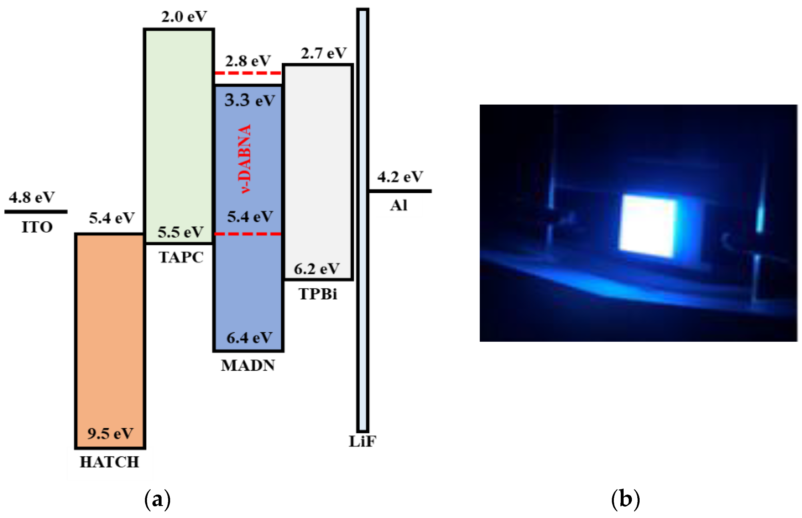
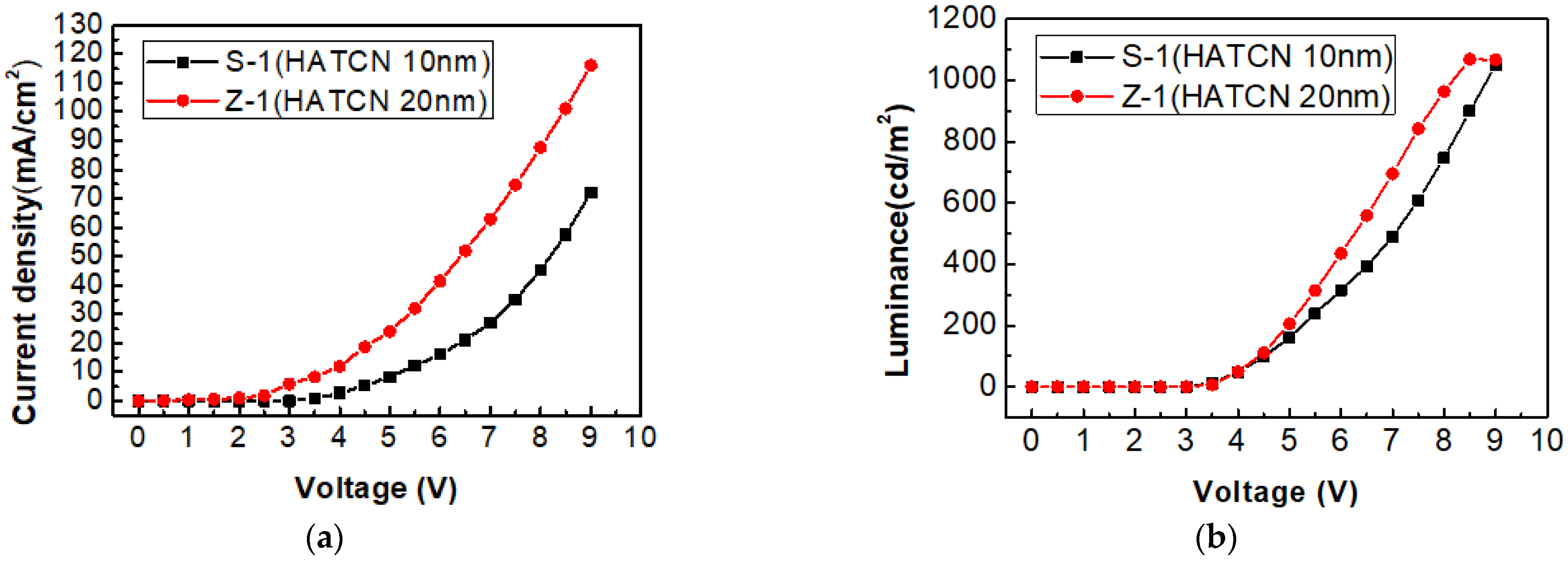
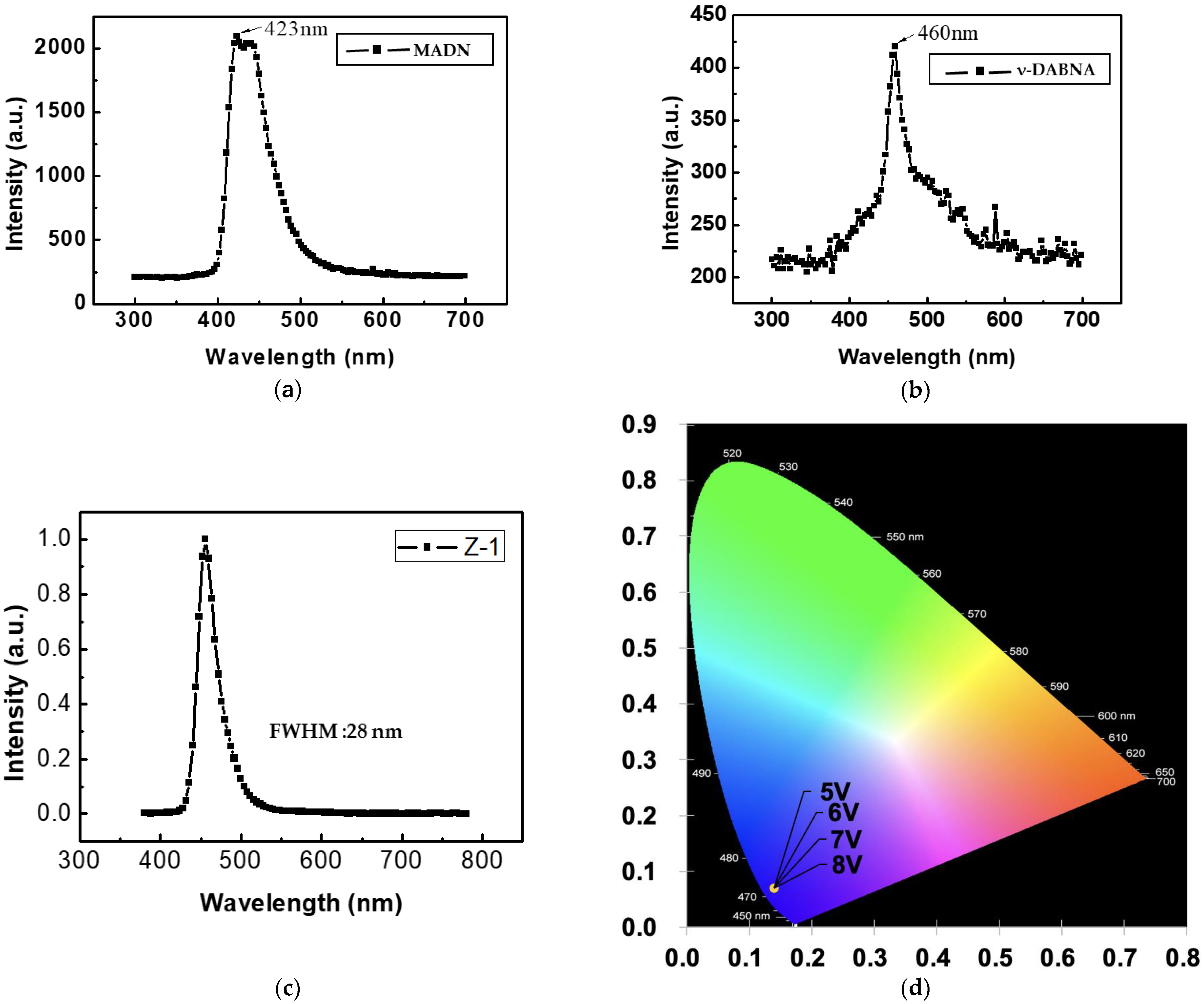
3.3. Blue OLED (BOLED) Devices

Blue OLED devices are fabricated through the adjustment of the hole injection layer (HIL) thickness and the effects of HIL thickness on the device characteristics are observed. In the beginning, we chose an ETL (TPBi) thickness, such as 30 nm. To obtain the optimal device structure, the HIL thickness needed to be adjusted to 10 and 20 nm, respectively. The structure of the blue OLED device was ITO/HATCN (Y nm)/TAPC (30 nm)/MADN: ν-DABNA (40 nm)/TPBi (30 nm)/LiF (0.8 nm)/Al (150 nm). Figure 11a depicts the energy band diagram of the blue OLED, and Figure 11b shows a photo of the blue emission. The device parameters of blue OLEDs are listed in Table 3. Figure 12a,b shows the current density–voltage and luminance–voltage characteristics, respectively. From the results, it was found that with an HATCN thickness of 10 nm the device had a current density of 45.29 mA/cm2 and luminance of 746.8 cd/m2 at 8 V. When the HATCN thickness was adjusted to 20 nm, the current density and luminance increased to 87.68 mA/cm2 and 963.9 cd/m2, respectively, at 8 V. Therefore, an HATCN of 20 nm was determined to be the best thickness.
The UV laser-excited photoluminescence (PL) analysis of the TADF host material MADN and the doped material ν-DABNA is shown in Figure 13a,b, respectively. This demonstrated that the host material MADN had a PL peak at about 423 nm, while the dopant peak ν-DABNA was at about 460 nm. The electroluminescence (EL) spectrum of the blue OLED Z-1 is shown in Figure 13c. From the EL spectrum in Figure 13c, it was apparent that the emission peak of an MADN doped with 10% ν-DABNA as the emitting layer was at 456 nm, and the full width at half maximum was only 28 nm. Based on Figure 13d, which shows the CIE coordinates, when MADN:ν-DABNA was used as the emitting layer, the CIE coordinates were fixed at (0.14, 0.07) when biased at 5–8 V, which was a pure blue device.

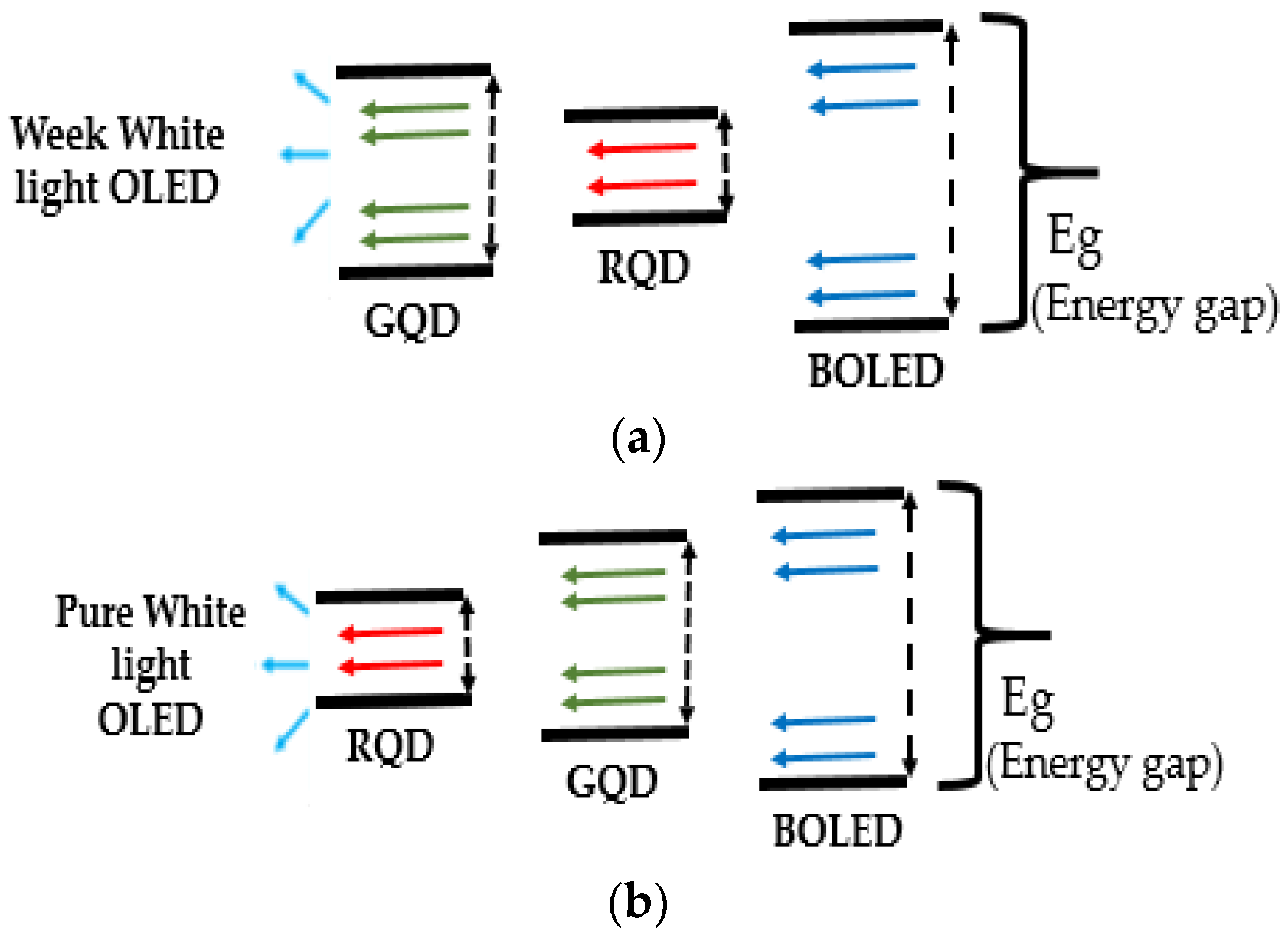
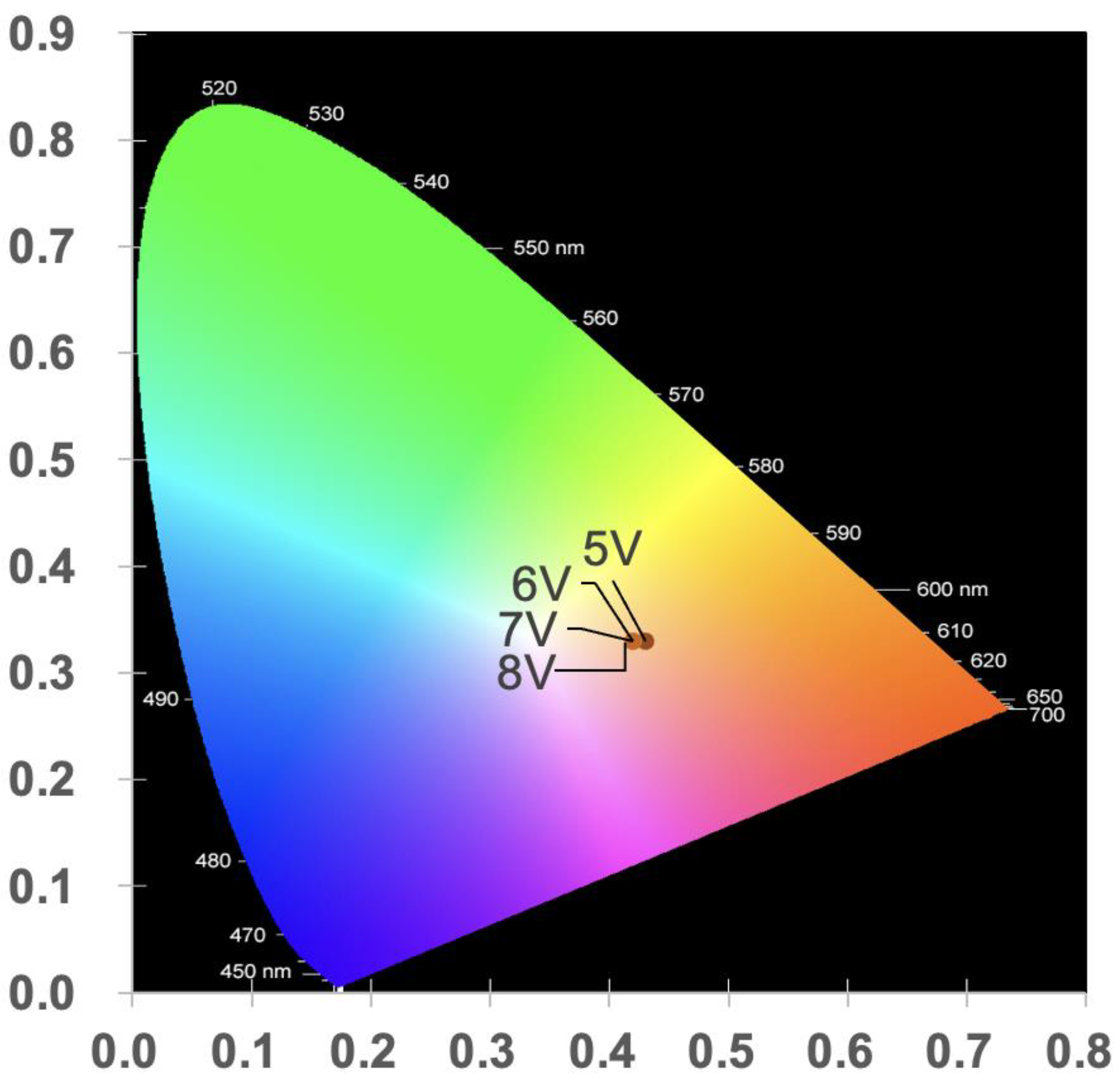
3.4. White OLED (WOLED) Devices

White OLEDs have numerous advantages; they differ from classical or even inorganic light sources in terms of their properties. For instance, they emit diffused light that can illuminate an area based on their ultrathin thickness [30]. The focus of this study was on developing a white OLED device using a QD PR. The QD PR was employed as the color conversion layer (CCL), which was excited by the blue OLED (BOLED). To fabricate the QD-based white light, a green QD and red QD color conversion film were sequentially bonded onto the backside of the blue OLED substrate.
To improve the white light chromaticity, two different light excitation architectures BOLED→GQD→RQD and BOLED→RQD→GQD were tested, as shown in Figure 14a,b, respectively. The first case was BOLED→GQD→RQD (blue light exciting GQD first) and the second case is BOLED→RQD→GQD (blue light exciting RQD first). Figure 15 illustrates the schematic device structure and the emitting photo of a white OLED.
However, luminance is related to lifetime, permanent burn-in, and power consumption. A high luminance requires a high luminous efficiency to avoid limiting lifetime and power consumption. Higher luminous efficiency means that a smaller current density is required for the same luminance. The WOLED has four subpixel structures. The white subpixel has high current efficiency, while red, green, and blue subpixels have low current efficiency. The filtering of primary colors results in almost 80 percent of light being lost while white light made by the stack of blue and yellow OLEDs passes through without being filtered [31,32]. From the study, to improve the optical efficiency of a white OLED display with a high color gamut, a red or green patterned QD film was used as a color converting component and an LPF was used as a light-recycling component. The QD film absorbed the unnecessary light from the white OLED, which was then cut by the CF to downconvert to the essential light, while the LPF reused the unnecessary light selectively to enhance the amount of light absorbed by the QD. In addition, to reduce reflection loss caused by an air gap, a refractive index matching liquid was utilized between the components [23,33]. In this study, the RQD or GQD was spin coated on a separate glass substrate different from the BOLED. The white light shown in Figure 15 was achieved by placing a nanaoimparted RQD or GQD PR on the back side of the BOLED glass substrate shown in Figure 14. Between the BOLED glass and the QD substrate, there was an air gap and reflection loss. The QD conversion efficiency excited by blue the OLED might be not high enough either. As a result, at an 8 V driving voltage, the BOLED light debilitated after exciting the (RQD) or (GQD). So in that case, the performance of white light (blue OLED mixed with RQD and GQD color conversion) was reduced when compared to a single-emitting layer blue OLED. Figure 16a,b illustrates the comparison of the luminance–voltage characteristic curve and electro luminance (EL) spectra at 8 V, respectively, for both white light excitation architectures. Based on both results, it was concluded that there was almost no difference in the luminance–voltage characteristics for both architectures.
Nevertheless, due to the energy gap architecture between BOLED→RQD→GQD, as shown in Figure 17a, most of the blue light energy from blue OLED was absorbed by the RQD because it was first excited, so the amount of blue light that reached the green QD was minimal. In addition, the excited red emission penetrated the GQD without exciting it. Therefore, pure white light was not able to be achieved since the green spectrum could not be excited as the red emission. The result is shown as the red curve in Figure 16b.
If the RQD-GQD order was reversed, the blue OLED first excited the GQD then the RQD, which resulted in three peaks emitting at 460, 530, and 620 nm at 8 V, as shown in Figure 16b. Due to the energy gap architectures between BOLED→GQD→RQD, as shown in Figure 17b, the green QD absorbed part of the blue light emitted from the BOLED, and the remaining blue light penetrated the GQD to reach the RQD. These excited spectra were very close to the white light, as the black square curve shows in Figure 16b. The original blue CIE coordinates were (0.15, 0.07). After using the excitation combination BOLED→GQD→RQD, the CIE coordinates were (0.42, 0.33), as shown in Figure 18, which was very close to the white light position and independent of the applied voltage.
QD (CdSe/ZnS)-based LEDs have been extensively studied in recent years, but very few approaches have been detailed for QD (CdSe/ZnS) PR-based white OLEDs. In the literature review, Maojun Yin et al., from Jilin University, used CdSe/ZnS quantum dot material mixed with polymethylmethacrylate (PMMA) to create a separate composite film to convert a blue OLED to white color, producing a white OLED with a maximum luminance of 10,250 cd/m2 and maximum current efficiency of 20.6 cd/A. In the case of the white OLED, the CIE coordinates shifted only from (0.291, 0.406) at 4 V to (0.288, 0.405) at 8 V. HyoJun Kim et al. from YONSEI University, South Korea, used red and green quantum dot materials mixed with PGMEA and positive photoresist and exposed and developed technology on the glass substrate to create a full-color OLED display. Jung Hyuk Im et al. Hongik University in South Korea investigated the color conversion properties of QD/OLEDs using the microcavity effect, with an OLED fabricated on a WO3/Ag/WO3 (WAW) anode. Some fabrication methods, such as drop casting, air-gapped bridges, QD dispersed PR films, and flat and patterned QD down-conversion films have been recognized for the development of the QD PR-based top and bottom emission white OLED on glass and PET substrates. In the development of QD PR-based WOLEDs, BLOEDs have played an important role. From the literature, all the research has been successful in achieving the white light. The QD nanoimprinting methods were introduced in this study to achieve QD PR-based white light emission. In that, the patterned sapphire was used as the master mold to prepare PDMS molds to be attached to spin-coated QD PR glass substrates to perform the nanoimprinting process. In that, the back side of a blue OLED was attached to nanoimprinted RQD and GQD photoresists, which were excited by blue OLEDs to achieve the white light. As a result of this process, we successfully fabricated GQD and RQD (CdSe/ZnS) PR-based bottom emission white OLEDs.

4. Conclusions

In this study, HATCN deposited over ITO was chosen as the HIL, and TAPC was used as the HTL as a match. HATCN/TAPC was employed to modify the surface of the ITO, enabling direct OLED fabrication without UV ozone or O2 plasma treatment. The electron and hole injection current became more balanced by adjusting the thickness of the ETL (TPBi) and the HIL (HATCN); optimal thicknesses were TPBi 30 nm and HATCN 20 nm, respectively.
The optimum blue OLED structure in this study was ITO/HATCN (20 nm)/TAPC (30 nm)/MADN: ν-DABNA (40 nm)/TPBi (30 nm)/LiF (0.8 nm)/Al (150 nm). The TADF series material MADN doped with 10% ν-DABNA was employed as blue EML with an emission peak at 456 nm and a very narrow FWHM of 28 nm. The emission area was 1 cm × 1 cm. The current density, luminance, and the current efficiency reached 87.68 cd/m2, 963.9 mA/cm2, and 1.10 cd/A, respectively, at 8 V. A white OLED device was successfully developed using green and red QD photoresists for the CCL, which was excited by the blue OLED. The bottom side of the blue OLED was attached to nanoimprinted RQD and GQD photoresists to achieve the white light OLED. In this project, two different blue light excitation architectures were tested: BOLED→GQD→RQD and BOLED→RQD→GQD. The EL spectra showed that the BOLED→GQD→RQD architecture had more strong green emissions (best performance) because the blue OLED excited the GQD PR first then the RQD PR. Due to the energy gap architectures between BOLED-GQD-RQD, the green QD absorbed part of the blue light emitted from BOLED, and the remaining blue light penetrated the GQD to reach the RQD. These excited spectra were very close to the white light, which resulted in three peaks emitting at 460, 530, and 620 nm. The original blue CIE coordinates were (0.15, 0.07). After the excitation combination, the CIE coordinates were (0.42, 0.33), which was close to the white light position.

Author Contributions

Conceptualization, H.-X.W. and C.-Z.J.; methodology and fabrication, H.-X.W., K.D.P. and J.-Y.C.; experiment and result validation, H.-X.W., K.D.P. and F.-S.J.; writing—original draft preparation, K.D.P. and H.-X.W.; writing—review and editing, K.D.P. and F.-S.J.; supervision and funding acquisition, F.-S.J. All authors have read and agreed to the published version of the manuscript.

Funding

The authors gratefully acknowledge the financial support provided by the Ministry of Science and Technology (MOST), Taiwan, under grant number MOST-109-2221-E-150-014 and MOST-110-2221-E-150-013.

Institutional Review Board Statement

Not applicable.

Informed Consent Statement

Not applicable.

Data Availability Statement

Data are contained within the article.

Acknowledgments

The authors thank Wen-Kai Kuo, Department of Electro-optical Engineering, National Formosa University, for supporting patterned sapphire for the nano-imprinting experiments.

Conflicts of Interest

The authors declare no conflict of interest.

References

  1. Leem, D.-S.; Kim, J.W.; Jung, S.O.; Kim, S.O.; Kim, S.H.; Kim, K.Y.; Kim, J.-J. Efficient and colour-stable hybrid white organic light-emitting diodes utilizing electron–hole balanced spacers. J. Phys. D Appl. Phys. 2010, 43, 405102. [Google Scholar] [CrossRef]
  2. Jeong, B.S. Device Modeling of Quantum Dot–Organic Light Emitting Diodes for High Green Color Purity. Appl. Sci. 2021, 11, 2828. [Google Scholar] [CrossRef]
  3. Yoon, C.; Kim, T.; Shin, M.H.; Song, Y.G.; Shin, K.; Kim, Y.J.; Lee, K. Highly luminescent and stable white light-emitting diodes created by direct incorporation of Cd-free quantum dots in silicone resins using the thiol group. J. Mater. Chem. C 2015, 3, 6908–6915. [Google Scholar] [CrossRef]
  4. Choi, M.K.; Yang, J.; Hyeon, T.; Kim, D.H. Flexible quantum dot light-emitting diodes for next-generation displays. Npj Flex. Electron. 2018, 2, 10. [Google Scholar] [CrossRef]
  5. Hu, Z.; Yin, Y.; Ali, M.U.; Peng, W.; Zhang, S.; Li, D.; Zhou, H. Inkjet printed uniform quantum dots as color conversion layers for full-color OLED displays. Nanoscale 2020, 12, 2103–2110. [Google Scholar] [CrossRef]
  6. Huang, Y.M.; Singh, K.J.; Liu, A.C.; Lin, C.C.; Chen, Z.; Wang, K.; Lin, Y.; Liu, Z.; Wu, T.; Kuo, H.C. Advances in Quantum-Dot-Based Displays. Nanomaterials 2020, 10, 1327. [Google Scholar] [CrossRef]
  7. Han, H.V.; Lin, C.C.; Tsai, Y.L.; Chen, H.C.; Chen, K.J.; Yeh, Y.L.; Yu, P. A Highly Efficient Hybrid GaAs Solar Cell Based on Colloidal-Quantum-Dot-Sensitization. Sci. Rep. 2014, 4, 5734. [Google Scholar] [CrossRef] [Green Version]
  8. Konstantatos, G.; Sargent, E.H. Solution-Processed Quantum Dot Photodetectors. Proc. IEEE 2009, 97, 1666–1683. [Google Scholar] [CrossRef]
  9. Pal, B.N.; Robel, I.; Mohite, A.; Laocharoensuk, R.; Werder, D.J.; Klimov, V.I. High-Sensitivity p–n Junction Photodiodes based on PbS nanocrystal quantum dots. Adv. Funct. Mater. 2012, 22, 1741–1748. [Google Scholar] [CrossRef]
  10. Koh, W.K.; Saudari, S.R.; Fafarman, A.T.; Kagan, C.R.; Murray, C.B. Thiocyanate-Capped PbS nanocubes: Ambipolar transport enables quantum dot based circuits on a flexible substrate. Nano Lett. 2011, 11, 4764–4767. [Google Scholar] [CrossRef]
  11. Algar, W.R.; Krull, U.J. Quantum dots as donors in fluorescence resonance energy transfer for the bioanalysis of nucleic acids, proteins, and other biological molecules. Anal. Bioanal. Chem. 2008, 391, 1609–1618. [Google Scholar] [CrossRef] [PubMed]
  12. Chen, K.J.; Lin, C.C.; Han, H.V.; Lee, C.Y.; Chien, S.H.; Wang, K.Y.; Chiu, S.H.; Tu, Z.Y.; Li, J.R.; Chen, T.M.; et al. Wide-Range correlated color temperature light generation from resonant cavity hybrid quantum dot light-emitting diodes. IEEE J. Sel. Top. Quantum Electron. 2015, 21, 23–29. [Google Scholar] [CrossRef]
  13. Armăşelu, A. Recent Developments in Applications of Quantum-Dot Based Light-Emitting Diodes. In Quantum-Dot Based Light-Emitting Diodes; IntechOpen: London, UK, 2017; pp. 7–24. [Google Scholar] [CrossRef] [Green Version]
  14. Kim, K.; Jung, H.; Bae, W.; Lee, C. Effect of Solvents and Pressure on the Performance of Quantum Dot light Emitting Diodes Fabricated with Soft-Contact Transfer Printing. SID Dig. 2018, 49, 1643–1646. [Google Scholar] [CrossRef]
  15. Yin, M.; Yu, Z.; Pan, T.; Peng, X.; Zhang, X.; Zhang, L.; Xie, W. Efficient and angle-stable white top-emitting organic light emitting devices with patterned quantum dots down-conversion films. Org. Electron. 2018, 56, 46–50. [Google Scholar] [CrossRef]
  16. Kim, H.-J.; Shin, M.H.; Kim, J.S.; Kim, S.E.; Kim, Y.J. High efficient OLED displays prepared with the air-gapped bridges on quantum dot patterns for optical recycling. Sci. Rep. 2017, 7, 43063. [Google Scholar] [CrossRef] [Green Version]
  17. Im, J.H.; Kang, K.T.; Choi, J.S.; Cho, K.H. Strong microcavity effects in hybrid quantum dot/blue organic light-emitting diodes using Ag based electrode. J. Lumin. 2018, 203, 540–545. [Google Scholar] [CrossRef]
  18. Lee, K.-H.; Han, C.Y.; Kang, H.D.; Ko, H.; Lee, C.; Lee, J.; Yang, H. Highly Efficient, Color-Reproducible Full-Color Electroluminescent Devices Based on Red/Green/Blue Quantum Dot-Mixed Multilayer. ACS Nano. 2015, 9, 10941–10949. [Google Scholar] [CrossRef]
  19. Li, Y.; Rizzo, A.; Mazzeo, M.; Carbone, L.; Manna, L.; Cingolani, R.; Gigli, G. White organic light-emitting devices with CdSe/ZnS quantum dots as a red emitter. J. Appl. Phys. 2005, 97, 113501. [Google Scholar] [CrossRef]
  20. Hao, J.; Liu, H.; Miao, J.; Lu, R.; Zhou, Z.; Zhao, B.; Xie, B.; Cheng, J.; Wang, k.; Delville, M.H. A facile route to synthesize CdSe/ZnS thick-shell quantum dots with precisely controlled green emission properties: Towards QDs based LED applications. Sci. Rep. 2019, 9, 12048. [Google Scholar] [CrossRef] [Green Version]
  21. Nguyen, H.T.; Pham, T.N.; Koh, K.H.; Lee, S. Fabrication and characterization of CdSe/ZnS quantum-dot LEDs. Phys. Status Solidi (A) 2012, 209, 1163–1167. [Google Scholar] [CrossRef]
  22. Heydari, N.; Ghorashi, S.M.B.; Han, W.; Park, H.H. Quantum Dot-Based Light Emitting Diodes (QDLEDs). New Progress. In Quantum-Dot Based Light-Emitting Diodes; IntechOpen: London, UK, 2017; pp. 25–45. [Google Scholar] [CrossRef] [Green Version]
  23. Kim, H.-J.; Shin, M.-H.; Hong, H.-G.; Song, B.-S.; Kim, S.-K.; Koo, W.-H.; Kim, Y.-J. Enhancement of Optical Efficiency in White OLED Display Using the Patterned Photoresist Film Dispersed with Quantum Dot Nanocrystals. J. Disp. Technol. 2016, 12, 526–531. [Google Scholar] [CrossRef]
  24. Dayneko, S.; Lypenko, D.; Linkov, P.; Sannikova, N.; Samokhvalov, P.; Nikitenko, V.; Chistyakov, A. Application of CdSe/ZnS/CdS/ZnS Core–multishell Quantum Dots to Modern OLED Technology. Mater. Today Proc. 2016, 3, 211–215. [Google Scholar] [CrossRef]
  25. Jeon, Y.P.; Park, S.J.; Kim, T.W. Electrical and optical properties of blue organic light-emitting devices fabricated utilizing color conversion CdSe and CdSe/ZnS quantum dots embedded in a poly(N-vibyl carbazole) hole transport layer. Opt. Mater. Express 2012, 2, 663. [Google Scholar] [CrossRef]
  26. Uoyama, H.; Goushi, K.; Shizu, K.; Nomura, H.; Adachi, C. Highly efficient organic light-emitting diodes from delayed fluorescence. Nature 2012, 492, 234–238. [Google Scholar] [CrossRef] [PubMed]
  27. Miwa, T.; Kubo, S.; Shizu, K.; Komino, T.; Adachi, C.; Kaji, H. Blue organic light-emitting diodes realizing external quantum efficiency over 25% using thermally activated delayed fluorescence emitters. Sci. Rep. 2017, 7, 284. [Google Scholar] [CrossRef] [Green Version]
  28. Rodella, F.; Saxena, R.; Bagnich, S.; Banevičius, D.; Kreiza, G.; Athanasopoulos, S.; Juršėnas, s.; Kazlauskas, K.; Köhler, A.; Strohriegl, P. Low efficiency roll-off blue TADF OLEDs employing a novel acridine–pyrimidine based high triplet energy host. J. Mater. Chem. C 2021, 9, 17471–17482. [Google Scholar] [CrossRef]
  29. Yin, X.; He, Y.; Wang, X.; Wu, Z.; Pang, E.; Xu, J.; Wang, J. Recent Advances in Thermally Activated Delayed Fluorescent Polymer—Molecular Designing Strategies. Front. Chem. 2020, 8, 725. [Google Scholar] [CrossRef]
  30. Ma, D. White OLED Devices. In Handbook of Advanced Lighting Technology; Springer: Cham, Switzerland, 2017; pp. 321–361. [Google Scholar] [CrossRef]
  31. Lee, J.H. QD Display: A Game-Changing Technology for the Display Industry. Inf. Disp. 2020, 36, 9–13. [Google Scholar] [CrossRef]
  32. Springer, R.; Kang, B.Y.; Lampande, R.; Ahn, D.H.; Lenk, S.; Reineke, S.; Kwon, J.H. Cool white light-emitting three stack OLED structures for AMOLED display applications. Opt. Express 2016, 24, 28131. [Google Scholar] [CrossRef]
  33. Kim, H.-J.; Shin, M.-H.; Kim, Y.-J. Optical efficiency enhancement in white organic light-emitting diode display with high color gamut using patterned quantum dot film and long pass filter. Jpn. J. Appl. Phys. 2016, 55, 08RF01. [Google Scholar] [CrossRef]
Figure 1. Schematic diagram of the following: (a) ITO engraved substrate; (b) organic evaporation area.
Applsci 12 06365 g001
Figure 2. RQD and GQD PR spin coating processes.
Applsci 12 06365 g002
Figure 3. Fabrication processes of nanoimprinting on the QD photoresist.
Applsci 12 06365 g003
Figure 4. Patterned sapphire: (a) SEM top view; (b) cross-sectional view and pyramid size.
Applsci 12 06365 g004
Figure 5. SEM surface photo of the patterned sapphire substrate: (a) 10,000 times magnification; (b) 30,000 times magnification.
Applsci 12 06365 g005
Figure 6. The chemical structures of (a) HATCN, (b) TAPC, (c) MADN, (d) ν-DABNA, (e) TPBi.
Applsci 12 06365 g006
Figure 7. Energy band diagram of the blue OLED for the modulating ETL material.
Applsci 12 06365 g007
Figure 8. (a) Current density–voltage and (b) luminance–voltage characteristic curves of the modulated ETL devices.
Applsci 12 06365 g008
Figure 9. Energy band diagram of hole-only devices with different HTL materials.
Applsci 12 06365 g009
Figure 10. Comparison of current density–voltage characteristics of hole-only devices with different HTL materials.
Applsci 12 06365 g010
Figure 11. (a) Energy band diagram; (b) the photo of blue emission of the BOLED.
Applsci 12 06365 g011
Figure 12. The blue OLED device: (a) current density–voltage characteristic curve; (b) luminance–voltage characteristic curve.
Applsci 12 06365 g012
Figure 13. UV laser-excited PL spectrum of the following: (a) MADN host luminescent material; (b) ν-DABNA dopant material; (c) EL spectrum of blue OLED Z-1; (d) CIE coordinates of blue OLED.
Applsci 12 06365 g013
Figure 14. Light excitation architectures of (a) BOLED→GQD→RQD and (b) BOLED→RQD→GQD.
Applsci 12 06365 g014
Figure 15. The schematic device structure and the emitting photo of a white OLED.
Applsci 12 06365 g015
Figure 16. (a) Luminance–voltage curves; (b) EL spectra of BOLED→GQD→RQD and BOLED→RQD→GQD.
Applsci 12 06365 g016
Figure 17. Energy band diagram of light excitation architectures: (a) BOLED→RQD→GQD; (b) BOLED→GQD→RQD.
Applsci 12 06365 g017
Figure 18. CIE coordinates of device assembly of BOLED→GQD→RQD.
Applsci 12 06365 g018
Table 1. Device parameters with modulated ETL materials (unit: nm).
DeviceHILHTL-1HTL-2EMLETLEILCathode
PEDOT: PSS (Spin)Poly-TPD(Spin)mCPMADN(90%): ν-DABNA (10%)XLiFAl
ET036Three layersOne layer1550200.8150
LG201
TmPyPB
TPBi
Table 2. Structural parameters of the hole-only devices with different HTL materials (unit: nm).
DeviceITOHILHTLEILCathode
UV TreatmentHATCNXLiFAl
TAPCYes10300.8150
TAPC (w/o UV)w/o
mCPYes15
mCP (w/o UV)w/o
Table 3. The device parameters of the blue OLED with its HATCN thickness adjusted (unit: nm).
HILHTLEMLETLEILCathode
NOHATCNTAPCMADN: ν-DABNA (10%)TPBiLiFAl
S-1103040300.8150
Z-120
Publisher’s Note: MDPI stays neutral with regard to jurisdictional claims in published maps and institutional affiliations.

